 M. Bruzzi
 N. Calisi3,4
 A. Vinattieri
95% of researchers rate our articles as excellent or good
Learn more about the work of our research integrity team to safeguard the quality of each article we publish.
Find out more
ORIGINAL RESEARCH article
Front. Phys. , 02 February 2023
Sec. Radiation Detectors and Imaging
Volume 11 - 2023 | https://doi.org/10.3389/fphy.2023.1126753
This article is part of the Research Topic Perovskite and Organic Materials for Radiation Detectors View all 5 articles
Introduction: This paper deals with the class of versatile semiconducting materials called perovskites, which have been deposited for the first time on flexible substrates and then tested for radiation detection monitoring applications.
Methods: Lead halide inorganic perovskite, CsPbCl3, 0.4–1 μm-thick films have been grown on plastic flexible substrates equipped with interdigitated electrodes (IDEs) by magnetron sputtering at room temperature.
Results: First measurements in realtime configuration are reported for a 1–µm thick prototype under proton beams with energy in the range 100–228 MeV and 1–10 nA extraction currents, of interest for protontherapy applications.
Discussion: Experimental results evidence good performances of our sample as a real-time monitoring device. Current stability under UV and proton beam exposure has been tested in the range 0.1–120 s, as well as reproducibility under multiple exposures. The measured current signal proved to be linearly dependent on the extraction currents at a given proton energy. Linearity of the current signal of the device with proton fluxes was also proved within two order of magnitude range, about 107–109 p/s. These promising results, when coupled with easyness of fabrication, low processing costs and high versatility of electrode configurations, all features characterizing the manufacturing process, put into evidence lead halide perovskites as promising candidates for real-time radiation detection in protontherapy.
Novel design strategies in radiation detection technology are recently moving towards thin, high-sensitivity and flexible solid-state devices especially characterized by low manufacturing costs and easy-processing. In this respect, the class of new and versatile semiconducting materials called perovskites is progressively experiencing an ever increasing scientific focus worldwide [1]. Perovskites include any material with the same type of crystal structure, ABX3, with A, B cations and X anion. In particular, metal-halide perovskites, mainly cesium lead halide (CsPbX3) and methylammonium lead halide (CH3NH3PbX3) attracted recently huge attention due to their improved optical and electrical properties. Unique physical properties of halide perovskites range from high-absorption coefficients, long-range ambipolar charge transport, high exciton-binding energy, high dielectric constant, all very attractive optoelectronic characteristics [2]. Growth from low-cost processes allows to manufacture them both as layered thin films, deposited on almost any kind of substrates and as single crystals of tailored size. Due to their strong stopping power, defect-tolerance, large mobility-lifetime product, high sensitivity per unit volume, halide perovskites were recently tested in several areas where stringent photodetection and dosimetric requirements are needed, as e.g. for medical imaging [3] radiation detectors [4, 5] and dosimeter [6–8]. Moreover, by opportunely varying the stoichiometry of the anion, starting from CsPbI3 towards CsPbBr3 and finally CsPbCl3, it is possible to finely tune the material bandgap from about 1 eV to 3 eV [9]. This feature provides access to a variety of different applications in photodetection and dosimetry. In particular, high-bandgap energy is an interesting feature for semiconductors in devices subject to harsh radiation environments, as the radiation induced lattice damage has no influence on the dark current of the detector [10].
This paper focuses on active devices used as real-time dosimeters for proton therapy. Their principle of operation is based on the continuous read-out, during irradiation, of the current, I, flowing between two electrodes supplied with a constant bias [11]. For a proper operation the current signal should be linearly dependent on the proton fluxes. To provide real-time beam monitoring in-vivo, the device should be operated in transmission during the dose delivery. In this condition, the thickness of the device should be minimized. To avoid a detrimental reduction of the sensitivity of the device, the active material should be characterized by a high sensitivity per unit volume. Recent results on inorganic halide perovskite detectors made of CsPbBr3 and CsPbCl3 [5, 7] evidenced sensitivity per unit volume for these materials of the same order or even higher than that of silicon, diamond and silicon carbide [11, 12], among the most semiconductors used for radiation detection purposes. With respect to CsPbBr3, CsPbCl3 seems to be characterized by a current response as a function of time during exposure to radiation less prone to instabilities due to defects or polarization effects [13–15]. Moreover, its high bandgap (3.0 eV) should provide less dark current making it an intrinsically radiation harder material, as in the case of SiC [16]. Moreover, there is an increasing interest in the scientific community for a flexible film dosimeter that can be attached to the irregular surfaces of a patient for in vivo dosimetry during radiotherapy [17]. In this respect, lead halide perovksite appear attractive, as they may be grown directly on any kind surfaces by low temperature magnetron sputtering techniques.
This paper shows first measurements carried out with CsPbCl3 thin film devices deposited on flexible substrates carrying interdigitated electrodes (IDE) when exposed to proton beams with energy in the range 100–228 MeV and extraction currents in the range 1–10 nA, of interest for proton therapy applications.
Cesium lead chloride (CsPbCl3) films have been grown by Radio Frequency (RF) magnetron sputtering on plastic substrates equipped with an array of Cu electrodes using a Korvus HEX (Korvus Technology Ltd.) sputter equipped with an RF source working at 13.56 MHz [18–20]. The precursor salts (CsCl and PbCl2) are grinded in equal molar ratio in a mixer mill (Retsch model MM400) to produce the powder used to manufacture the sputtering target: a 5 cm diameter disk realized by pressing the perovskite powder by means of a pneumatic press (11.5 MPa working pressure) for 24 h at 150°C [21]. The deposition is carried out at room temperature with 20 W RF power and with a 20 sccm argon gas flow. Dynamic working pressure is 2 × 10⁻⁶ atm, deposition rates are in the range 5–7 × 10⁻² nm/s. The sample is nominally undoped even if unwanted p-doping is due to Cs vacancies [22]. The film thickness is monitored during growth by means of a quartz crystal microbalance. During deposition the sample holder rotates to ensure thickness homogeneity across the substrate.
A detailed electro-optical characterization of CsPbCl3 thin films, deposited with the same technique on glass, has been reported elsewhere [13, 20]. Room temperature transmittance spectrum provided a value of the bandgap of 3.0 eV. Room temperature XRD spectra indicate the presence of the correct crystalline phases CsPbCl3 (ICDD PDF-4+ 18-0366), orthorhombic and tetragonal crystalline phases [13]. SEM analyses reported in [20] evidences a film morphology characterized by a continuous network of several tens of nanometer size crystals with a random distribution of bigger crystals with typical micrometer/sub-micrometer size. I-V characteristics performed with samples of different thickness on glass substrates, from 100 nm to 1.5 μm indicate a good homogeneity of the semiconductor material independently of the deposition time [21]. Thermally stimulated currents after exposure with a 365 nm LED priming measured from room temperature up to 370 K showed no evidence of trapping effects due to intragap states on the electrical transport properties at room temperature of the films. As a consequence, measured photocurrents at room temperature appear to be stable in time with negligible priming effects.
With the purpose of prototyping first flexible thin film real-time detectors based on inorganic perovskite, we have deposited with the same technique a set of CsPbCl3 films on PET substrates equipped with interdigitated electrodes (IDEs). Figure 1A shows the sample, named #7, tested in this study under proton beam, carrying a CsPbCl3 film 1 μm-thick deposited on the whole interdigitated electrode array of a flexible plastic substrate (PW-IDEPD100 by DropSens). The two interdigitated electrodes have 100 µm bands/gaps pitches and 5 × 7 mm2 total area and nominal 175 μm thickness. The prototype is especially designed to get high electric signals starting from rather low thickness of material on a decentralized assay in planar electrode configurations. In the whole, the device is equipped with 35 pairs of contacts, 5 mm-long each: active area is 5.0 × 3.5 mm2. To perform electrical measurements, the two connection tracks of the IDEs are directly connected to coaxial cables via sliding contacts. A pristine IDE substrate, #14, without the CsPbCl3 thin film deposition, has been also prepared in same conditions, to be used as a reference during proton beam tests. The electrode termination are connected to Keithley 6517A/B high resistance source/electrometers, used both to supply an external voltage and to read-out the current, typically in the range 100nA-0.1 pA. The internal circuit of the instrument allows to monitor the current in real-time with varying integration times in the range 3–100 ms depending on the specifically investigated current ranges.
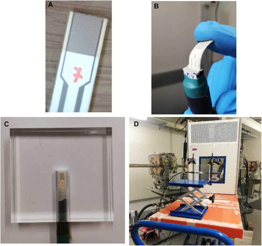
FIGURE 1. (A) 1 μm-thick CsPbCl3 thin film deposited by magnetron sputtering on the plastic substrate equipped with Pd interdigitated electrodes (IDEs). Same device: (B) with insulating envelop to avoid for ionized air contribution, bending under tiny deformation stress; (C) inserted in the cylindric hole of a PMMA phantom slab and (D) placed at the beam isocenter of the TIFPA experimental line.
The response of the two devices during irradiation has been tested at the proton therapy center in Trento, Italy, which is part of the Trentino Healthcare Agency (Azienda Provinciale per i Servizi Sanitari—APSS, Italy). A cyclotron (IBA, Proteus 235) serves two medical treatment rooms both equipped with rotating gantries. Our test has been carried out at the experimental area, whose activity is managed and supervised by Trento Institute for Fundamental Physics and Applications (TIFPA) of the National Institute for Nuclear Physics (INFN). The total energy range of the proton therapy facility is 70–228 MeV, typical treatments fluxes are in the range 106–109 p/s [23].
After a preliminary optical and electrical characterization of the devices, we have measured in real-time configuration the current response of our devices to proton beams with energy in the range 100–228 MeV and extraction currents in the range 1–10 nA. During tests under the proton beam, the prototypes, including its electrode terminations, has been sealed into an insulating envelope to avoid unwanted current contributions due to the ionized air close to electrodes. Our configuration still allows for sample flexibility. Picture in Figure 1B shows the sample under test, #7 within its insulating envelope, bending under a tiny mechanical stress. The devices have been encapsulated in a 10 × 10 cm2 PolyMethylMethAcrylate (PMMA) slab 1 cm thick (see Figure 1C) within a cylindric hole of the same diameter of the sliding contacts connector (1.3 cm), ensuring sample flexibility. The PMMA phantom has been placed at the isocenter of the beam at the TIFPA experimental line (see Figure 1D). During the proton test beam the flexible sample has been always kept in planar configuration.
The proton flux per unit extraction current (1 nA) impinging on the detector area is plotted as a function of the proton beam energy in Figure 2, together with an exponential best-fit to data shown as a guide-line. The fraction of protons reaching the detector has been estimated by integrating the beam profile, essentially Gaussian, on the detector area:
where a and b are the lateral dimensions of the detector and
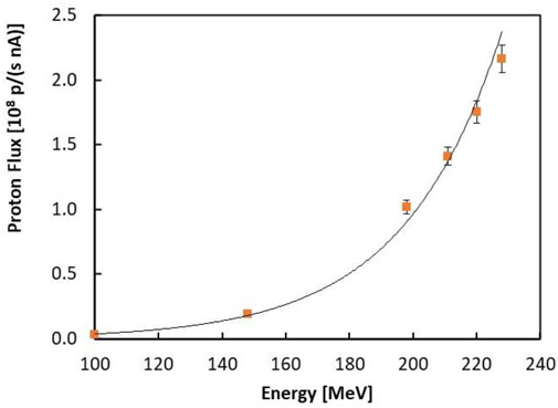
FIGURE 2. Proton flux incident on the detector area per unit extraction current (1 nA) plotted as a function of the proton beam energy. Exponential best-fits is shown only for guide-line purposes.
Preliminary optical and electrical characterization of the films deposited on the flexible interdigitated electrodes have been performed at room temperature (T = 21°C). Photoluminescence (PL) experiments have been performed after excitation with a 266 nm laser with an excitation power of 10 mW: the PL has been dispersed by a spectrograph (Kymera 193i Andor Corp.) and detected by a CCD camera (IDUS 401 Andor Corp). PL spectra for a set of five samples with different thicknesses are shown in Figures 3A, B. The indication of treated sample means a thermal annealing at 150°C for 20 h. The plots evidence no major differences depending on the film thickness and thermal treatment in the PL intensity and lineshape. Results are in agreement with those found with similar samples grown on glass substrates [13].
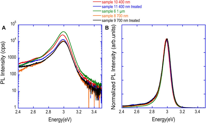
FIGURE 3. Photoluminescence spectra (PL) spectra for the different samples: in (A) the intensity is shown in log scale, in (B) normalized spectra are reported for a comparison of the lineshape.
Current Voltage (IV) characterization of our devices in dark have been also performed. In particular, Figure 4A shows the dark current of the 1 μm-thick CsPbCl3 film deposited on the Pd IDEs as a function of time, measured along a 2 min interval with different applied voltages. The plot evidences the stability in time of the measured current. Figure 4B shows the average current measured as a function of the voltage at 21°C in the range 1–5 V. The measurements have been carried with the device in planar configuration. Further I-V measurements done after bending the sample for 1 min with a curvature radius of 7 mm along the longer size of the device showed changes in the I-V characteristics within 2%. The ohmic behavior of the device is evidenced by the linear best-fit to data; the resistance calculated from the slope of the curve is about 7 × 10⁹ Ω. Taking into consideration geometry and thickness of the device, from these data we get a room temperature resistivity ρ = 1.2 × 10⁷ Ω m, in good agreement with Ref. [13].
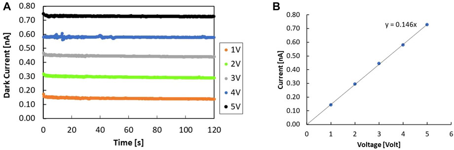
FIGURE 4. (A) Dark current of the 1 μm-thick CsPbCl3 film deposited on Pd IDEs as a function of time measured at room temperature and different applied voltages. (B) Average currents plotted as a function of the voltage, with linear best fit.
Figure 5 shows the response of the same device to a train of square pulses from a 365 nm UV lamp with frequency of 1 Hz and intensity 100 W/m2 at different applied voltages (10-5-2 V), for an interval of 30 s at sampling times of 100 ms. The plot shows a stable and repeatible photoconductive transient response, with rise and decay times in the range of 0.1 s or less on the entire time interval and amplitude linerly increasing with the applied voltage.
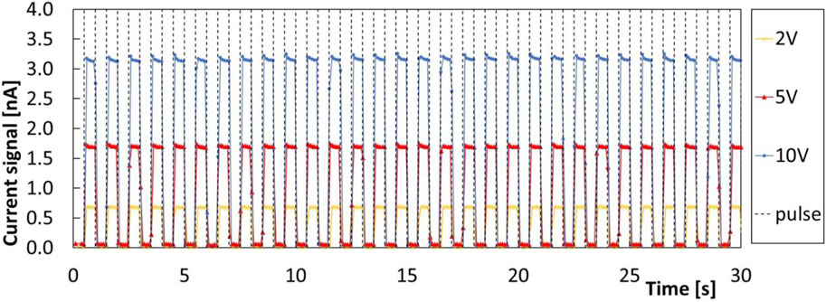
FIGURE 5. Current signal of the 1 μm-thick CsPbCl3 film deposited on the Pd IDEs due to the excitation of a train of square pulses from a 365 nm UV LED lamp with frequency of 1 Hz and intensity 100 W/m2. Measurements are carried out at different applied voltages and sampling time windows of 100 ms.
After this preliminary characterization we have measured the current response of the same prototype, #7, under proton beams of different energy and extraction current operation. Figure 6 shows the current measured with the same prototype, #7, under exposure to a 220 MeV proton beam and extraction currents values progressively decreasing: 10-5-2-1 nA. To evidence a possible contribution to the signal due to the interdigitated electrodes and PET substrate, the same measurement has been performed using a device with same packaging, electrodes and substrate but no perovskite film deposited on it (#14). The current response of device #14 in exactly the same conditions as #7 is shown in the same plot of Figure 6. From the plot we observe that a current signal is collected also by the interdigitated electrode substrate without the perovskite film, probably due to the polarization of the plastic substrate. Anyway, this signal is definitely lower than those measured in the same conditions by device #7, carrying the CsPbCl3 1 μm-thick film. In fact, by comparing results of the #7 and #14 devices, we get that the perovskite thin film current contribution is about 3.5 times that due to the substrate. Moreover, we observe that instabilities in the current response, as the slow rise-time observed when the beam is switched on, especially at highest extraction currents (10 nA), and current oscillations during measurements, are not due to the perovskite film itself, but should rather to be considered as instrumental effects due to the coupling of the read-out electronics of the high-impedance multimeter and the IDE/Pd substrate.
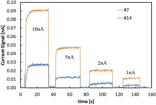
FIGURE 6. Current response of the sample prototype #7, carrying the 1 μm-thick CsPbCl3 film on the IDE/Pd substrate measured and of prototype #14, without the CsPbCl3 film on the same substrate, plotted as a function of time under exposure to a 220 MeV proton beam using different extraction currents: 10-5-2-1 nA (dark current subtracted, applied voltage V = 2 V).
After these evidences, further measurements we have been focused on the current response of the prototype carrying the CsPbCl3 film. Figure 7 shows the average signals measured by the device as a function of the extraction current respectively for 220MeV and 198 MeV. The current signal is obtained by subtracting the dark current to the measured current. Best-fits to data, also shown, give evidence of the linear dependence of the signal on the extraction currents for each proton energies.
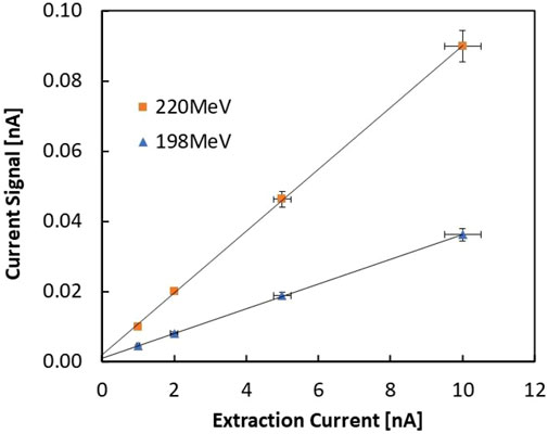
FIGURE 7. Average signals measured by the #7 (1 μm-thick CsPbCl3 on IDE/Pd) prototype as a function of the extraction current respectively under exposure of three different proton beam energies, applied voltage = 2 V.
Figure 8 shows the current signal (dark current subtracted) of the same prototype, #7, measured at same extraction current, 10 nA, and four different proton beam energies, 198-211-220 and 228 MeV, same exposure time interval, Δt = 110 s and same applied voltage across electrodes (2 V).
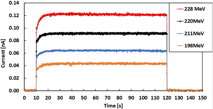
FIGURE 8. Current signals measured by the #7 prototype 1 μm-thick CsPbCl3 on IDE/Pd substrate, as a function of time for different proton beam energies and same extraction current, 10 nA. Applied voltage across electrodes is V = 2 V.
Figure 9 shows the average current signals measured in this experiment plotted as a function of the proton fluxes calculated at each proton energy for 10 nA extraction currents. Values of the corresponding effective proton fluxes are obtained considering the plot given in Figure 2 and multipling by the extraction current. Best-fit to data indicates a linear dependence of the current of our device on the proton flux.
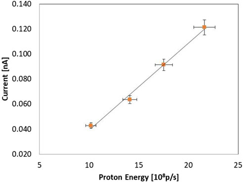
FIGURE 9. Average current measured by the 1 μm-thick CsPbCl3 IDE/Pd prototype #7 (applied voltage V = 2 V) as a function of the proton fluxes corresponding to the beam energies 198-211-220–228 MeV and same extraction current (10 nA), polynomial fit added as a guide-line.
Finally, Figure 10 shows in a log-log plot the average current signal (dark current subtracted) measured during a set of 20 different measurements carried out with different proton energies and extraction currents, varied respectively in the ranges 100–228 MeV and 1–10 nA. Values of the corresponding effective proton fluxes impinging on the detector area have been obtained by Eq. 1 (see Figure 2) and multipling by the corresponding extraction currents. The best fit to data evidence a linear trend on almost a two-order magnitude scale for proton fluxes in the range 4x10⁷ to 2 × 10⁹ p/s.
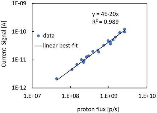
FIGURE 10. Average current measured by the 1 μm-thick CsPbCl3 IDE/Pd prototype, #7 (applied voltage V = 2 V) as a function of the proton flux impinging on the detector area, measred at different energies and extraction currents, respectively in the ranges 100–228 MeV and 1–10 nA. Best-fit to data shows a linear trend.
This paper shows first lead halide CsPbCl3 thin film deposition on flexible PET substrates carrying interdigitated electrodes (IDE) for sensor developments. The CsPbCl3 thin films have been deposited by magnetron sputtering at room temperature by means of a one-step process on IDEs made with Pd on plastic substrates (CsPbCl3/Pd IDE). First measurements of these prototype sensors in real-time configuration are reported under test beam with proton energy in the range 100–228 MeV and extraction currents in the range 1–10 nA, of interest for proton therapy applications. Experimental results evidence the good performances of the CsPbCl3/Pd IDE in terms of real-time monitoring, linearity with current extraction and proton fluxes in almost two orders of magnitude range, 4x10⁷—2 × 10⁹ p/s. These promising results, when coupled with easyness of fabrication, low processing costs and high versatility of electrode configurations, all features characterizing our manufacturing process, put into evidence lead halide perovskite, CsPbCl3, as a promising candidate for future radiation monitoring in protontherapy.
The original contributions presented in the study are included in the article/Supplementary Material, further inquiries can be directed to the corresponding author.
Conceptualization, MB and AV; methodology, MB, AV, and EV; software, MB and EV; device manufacturing MB, and NC; validation, MB, AV, and EV; formal analysis, MB, EV, and AV; investigation, MB, EV, NE, and AV; resources, MB; data curation, MB and EV; writing—original draft preparation, MB; writing—review and editing, MB, AV, and EV; supervision, MB and AV; project administration, MB; funding acquisition, MB.
Work performed in the framework of the experiment ANEMONE financed by Istituto Nazionale di Fisica Nucleare, CSN5-INFN, Italy.
The authors declare that the research was conducted in the absence of any commercial or financial relationships that could be construed as a potential conflict of interest.
All claims expressed in this article are solely those of the authors and do not necessarily represent those of their affiliated organizations, or those of the publisher, the editors and the reviewers. Any product that may be evaluated in this article, or claim that may be made by its manufacturer, is not guaranteed or endorsed by the publisher.
1. Brenner TM, Egger DA, Kronik L, Hodes G, Cahen D. Hybrid organic-inorganic perovskites: Low-cost semiconductors with intriguing charge-transport properties. Nat Rev Mater (2016) 1:15007. doi:10.1038/natrevmats.2015.7
2. Kovalenko MV, Protesescu L, Bodnarchuk MI. Properties and potential optoelectronic applications of lead halide perovskite nanocrystals. Science (2017) 358:745–50. doi:10.1126/science.aam7093
3. Zhou Y, Chen J, Bakr OM, Mohammed OF. Metal halide perovskites for X-ray imaging scintillators and detectors. ACS Energ Lett (2021) 6:739–68. doi:10.1021/acsenergylett.0c02430
4. Wei H, Huang J. Halide lead perovskites for ionizing radiation detection. Nat Commun (2019) 10:1066. doi:10.1038/s41467-019-08981-w
5. He Y, Stoumpos CC, Hadar I, Luo Z, McCall KM, Liu Z, et al. Demonstration of energy-resolved γ-ray detection at room temperature by the CsPbCl3 perovskite semiconductor. J Am Chem Soc (2021) 143(4):2068–77. doi:10.1021/jacs.0c12254
6. Bruzzi M, Talamonti C, Calisi N, Falsini N, Vinattieri A. First proof-of-principle of inorganic perovskites clinical radiotherapy dosimeters. Phys Lett Mater (2019) 7:051101. doi:10.1063/1.5083810
7. Bruzzi M, Calisi N, Latino M, Falsini N, Anna V, Talamonti C. Magnetron sputtered CsPbCl3 perovskite detectors as real-time dosimeters for clinical radiotherapy. Z für Medizinische Physik (2022) 32:392–402. doi:10.1016/j.zemedi.2022.02.003
8. Bruzzi M, Talamonti C. Characterization of crystalline CsPbBr3 perovskite dosimeters for clinical radiotherapy. Front Phys (2021) 9:625282. doi:10.3389/fphy.2021.625282
9. Ghaithan HM, Alahmed ZA, Qaid SMH, Aldwayyan AS. Density functional theory analysis of structural, electronic, and optical properties of mixed-halide orthorhombic inorganic perovskites. Inorg Perovskites (2021) 6(45):30752–61. doi:10.1021/acsomega.1c04806
10. Bruzzi M, Sadrozinski HF-W, Seiden A. Comparing radiation tolerant materials and devices for ultra rad-hard tracking detectors. Nucl Instr Meth Phys Res A (2007) 579(2):754–61. doi:10.1016/j.nima.2007.05.326
11. Bruzzi M. Novel silicon devices for radiation therapy monitoring. Nucl Instr Meth Phys Res A (2016) 809:105–12. doi:10.1016/j.nima.2015.10.072
12. Owens A, Peacock A. Compound semiconductor radiation detectors. Nucl Instr Meth Phys Res A (2004) 531:18–37. doi:10.1016/j.nima.2004.05.071
13. Bruzzi M, Latino M, Falsini N, Calisi N. A Vinattieri electrical and optical characterization of CsPbCl3 films around the high-temperature phase transitions. Nanomaterials (2022) 12(3):570–2022. doi:10.3390/nano12030570
14. Bruzzi M, Gabelloni F, Calisi N, Caporali S, Vinattieri A. Defective states in micro-crystalline CsPbBr3 and their role on photoconductivity. Nanomaterials (2019) 9(2):177. doi:10.3390/nano9020177
15. Bruzzi M, Calisi N, Falsini N, Vinattieri A. Electrically active defects in polycrystalline and single crystal metal halide perovskite. Energies (2020) 13(7):1643. doi:10.3390/en13071643
16. Bruzzi M, Nava F, Russo S, Sciortino S, Vanni P. Characterisation of silicon carbide detectors response to electron and photon irradiation. Diamond Relat Mater (2001) 10:657–61. doi:10.1016/s0925-9635(00)00380-0
17. Cho JD, Son J, Sung J, Choi CH, Kim JS, Wu H-G, et al. Flexible film dosimeter for in vivo dosimetry. Med Phys (2020) 47(7):3204–13. doi:10.1002/mp.14162
18. Seth S, Samanta A. A facile methodology for engineering the morphology of CsPbX3 perovskite nanocrystals under ambient condition. Sci Rep (2016) 6:37693. doi:10.1038/srep37693
19. Borri C, Calisi N, Galvanetto E, Falsini N, Biccari F, Vinattieri A, et al. First proof-of-principle of inorganic lead halide perovskites deposition by magnetron-sputtering. Nanomaterials (2019) 10:60. doi:10.3390/nano10010060
20. Falsini N, Calisi N, Roini G, Ristori A, Biccari F, Scardi P, et al. A new route for caesium lead halide perovskite deposition. Nanomaterials (2021) 11:8. doi:10.1186/s41476-021-00153-y
21. Falsini N, Ristori A, Biccari F, Calisi N, Roini G, Scardi P, et al. A new route for high quality nanometric films of inorganic halide perovskites. J Eur Opt Soc.-Rapid Publ (2021) 17:07004. doi:10.1051/epjconf/202023807004
22. Wu H, Pi J, Zhou D, Wang Q, Long Z, Qiu J. Effect of cation vacancy on lattice and luminescence properties in CsPbBr3 quantum dots. Ceramics Int (2022) 48:3383–9. doi:10.1016/j.ceramint.2021.10.114
Keywords: lead halide perovskite, CsPbCl3, detectors, dosimeters, proton therapy, RF magnetron sputtering
Citation: Bruzzi M, Calisi N, Enea N, Verroi E and Vinattieri A (2023) Flexible CsPbCl3 inorganic perovskite thin-film detectors for real-time monitoring in protontherapy. Front. Phys. 11:1126753. doi: 10.3389/fphy.2023.1126753
Received: 18 December 2022; Accepted: 17 January 2023;
Published: 02 February 2023.
Edited by:
Ge Yang, North Carolina State University, United StatesReviewed by:
Petro Fochuk, Chernivtsi University, UkraineCopyright © 2023 Bruzzi, Calisi, Enea, Verroi and Vinattieri. This is an open-access article distributed under the terms of the Creative Commons Attribution License (CC BY). The use, distribution or reproduction in other forums is permitted, provided the original author(s) and the copyright owner(s) are credited and that the original publication in this journal is cited, in accordance with accepted academic practice. No use, distribution or reproduction is permitted which does not comply with these terms.
*Correspondence: M. Bruzzi, bWFyYS5icnV6emlAdW5pZmkuaXQ=
Disclaimer: All claims expressed in this article are solely those of the authors and do not necessarily represent those of their affiliated organizations, or those of the publisher, the editors and the reviewers. Any product that may be evaluated in this article or claim that may be made by its manufacturer is not guaranteed or endorsed by the publisher.
Research integrity at Frontiers
Learn more about the work of our research integrity team to safeguard the quality of each article we publish.