 Yichu He1,2†
 Zeshu Wang1,2†
 Zi Wang1,2†
 Guan-Hua Dun1,2
 Xiangshun Geng1,2Chunlin Wang1,2Jingbo Du1,2Tianyu Guo1,2Dan Xie1,2*
 He Tian1,2*
 Yi Yang1,2*Tian-Ling Ren1,2*
- 1School of Integrated Circuits, Tsinghua University, Beijing, China
- 2Beijing National Research Center for Information Science and Technology (BNRist), Tsinghua University, Beijing, China
Perovskite-based X-ray detector, which is widely applied in fields of scientific research and medical diagnosis, has drawn much attention for its superior optoelectrical properties. To improve the detection performance, band engineering is becoming the hot topic for perovskite properties modulation. In this article, we review the recent progress of perovskite-based X-ray detectors with band engineering process from three aspects, which are background introduction, band theory of heterojunction devices, and optimized electrode contact devices. Lastly, research status and strategies are summarized and perspectives of future progress are analyzed. We hope this review can provide constructive instructions and suggestions for future development of band engineering for perovskite-based high-performance X-ray detector.
1 Introduction
X-ray detection, which transfers X-ray irradiance to measurable current signals, is attracting much attention for its wide application from space exploration, scientific research, flaw detection to people’s daily life, say medical X-ray imaging. The X-ray source, however, may impact on human health and damage the equipment due to radiation leakage. Hence, X-ray detector with high sensitivity and response speed is expected [1]. In terms of pattern in which X-ray are converted into electrical signals, direct conversion detection exhibits higher efficiency than indirect one. Because of direct conversion effect, X-ray signals can be transferred to current signals directly for reinforced transportation of electrons and holes under external bias [2], for which signal-noise ratio (SNR) and response time can be reduced. X-ray detection materials are proven to show such qualities as: (1) heavy atoms for efficient X-ray absorption; (2) high resistivity and low dark current to make device with low leakage [3]; (3) relatively high μτ product to facilitate the transportation and collection of carriers. μ and τ represent carrier mobility and carrier lifetime respectively [4]; (4) considerable stability [5]. The device should be persistent enough to maintain a low surface leakage current.
Recently, metal halide perovskite (MHP) has drawn much attention to X/gamma-ray detection ascribing to its attractive composition and superior physical properties. Intrinsically, the composition and structure based on MHP are reconfigurable for low power [6, 7]. And great tolerance of material itself is exhibited for high impurity states to realized a long-term working time. In terms of fabrication, MHP is compatible with Si fabrication for pixelation integration and can be conducted at room temperature at a bargain price. Besides, high resolution and sensitivity of MHP open a avenue for X-ray detector of high performance. Nowadays, the maximum sensitivity of perovskite X-ray detectors exceeds that of commercial α-Se-based X-ray detectors by 6-7 orders of magnitude, which is significantly lower than the dose-rate standard required for medical imaging [8, 9].
Though perovskite X-ray detector has fulfilled current requirements from the perspective of sensitivity and detection, stability remains a major obstacle to its commercial application. One of the most difficult challenges affecting the stability of perovskite is ion migration in the very material. Notably, ion migration is directly related to the surface defects [10]. In perovskite crystals, ion migrates through Schottky defects, Frankel defects and other defects. Especially for polycrystalline films, the grain boundary and crystal surface are relatively open. In addition to point defects, the activation energy is lower than that in the crystal. Accordingly, the grain boundaries are significant channels for ion migration. Undesirable defects and surface trap states will considerably aggravate current drift and dark current.
Hence, by constructing the same dimension perovskite heterojunction, suboptimal carrier transport characteristics caused by defects can be improved. For instance, a lateral grown pn heterojunction of p-type CH3NH3PbBr3(MAPbBr3)/n-type CH3NH3PbCl3(MAPbCl3) can effectively passivate surface defects of pristine materials due to excellent and robust lattice matching [11]. Besides, the designed heterojunction endows the existence of built-in electric field and further reduces dark current to perform a favorable carrier transport characteristic, which guarantees for excellent photoelectric performance.
As for perovskite single crystals (SC), the ion migration barrier is generally increased by passivation of halogen vacancy [12]. For example, the ion migration of Cs2AgBiBr6 is inhibited by heteroepitaxy BiOBr growth so that the signal drift of X-ray detector prepared by BiOBr is three orders of magnitude lower than that of previous detectors [13]. For polycrystalline thick film (over 1 μm) [14], similar effect can be realized by increasing the density of polycrystalline film to reduce the cavity, passivate grain boundaries and introduce the quasi two-dimensional structure of dark current [15], adding suitable polymer barrier layer and so on. Additionally, organic amine ion inhibition can also be introduced [16], which increases the ion migration barrier by increasing the chain length.
High sensitivity and low dose rate of 3D perovskite X-ray detectors promise an expected platform to study intrinsic characteristic of material and attracts increasingly attention [17]. Disappointingly, three-dimensional perovskite has the limitation of tolerance factor, leading to the obstacle of instability [18]. The presence of three-dimensional perovskites limit the serve life of the products and hampers the desire to significantly reduce the X-ray dose in medical imaging. Surprisingly, 2D perovskite counterparts separated from long-chain organic cations reveal advanced features in suppressing ion migration, which is at large applied bias. Therefore, in recent years, the establishment of heterogeneous structures with different dimensions is also one of the most effective and widely used means to settle the instability problem of perovskites [7]. At present, abundant new heterojunction perovskite materials with diverse composition and structural dimensions, such as 2D (FPEA)2PbBr4/3D FAPbBr3 fabricated through epitaxy growth method, have been reported [19].
Integrating three-dimensional with two-dimensional perovskite materials make it possible to realize a X-ray detector material with high carrier mobility [20], large exciton binding energy and large μτ product [3, 4]. And reliable stability [5], effective charge transfer and tunable band gap [6] with different number of layers guarantee that the mixed perovskite X-ray detector has great potential in preferred properties.
In the context, this work aims to review previous explorations on the optimization of perovskite-based X-ray detectors through energy band engineering, which is an efficient carrier management strategy. To overcome MHPs’ intrinsic limitations such as impurity detects, ions migration, it is a profound way to improve the combination of different heterojunctions. This paper involves two parts: the band engineering with heterojunction and the energy band optimization of the contact with metal electrodes. By retrospecting the energy band characteristics after the integration of different materials and summarizing their alterable characteristics, it is expected to provide guidance for the fabrication of X-ray detectors in the future, as well as the design and preparation of other materials such as LED, solar cells etc., so as to achieve photoelectric conversion with higher performance and accelerate the application and development of perovskites in years to come.
2 Band engineering theory
The band engineering of semiconductors can be categorized into two aspects [21, 22]:
one refers to bandgap pattern engineering. By means of doping, energy band structure can be modified to modulate the transportation of carriers a great extent, resulting in high detection performance. Another is bandgap structure engineering. Semiconductors with different bandgap can be tailored to influence the transportation of charge carriers between materials, for which the optoelectronic (electric and optical) properties can be optimized.
2.1 Bandgap pattern engineering with doping process
Rational doping methodology is meaningfully demanded to optimize the performance of materials. With the development of semiconductor engineering and the profound study of doping for band structure tailoring, it is found that dopant provides perovskite intrinsic layer with electrons while the ionized impurities work as scattering center to promote electron migration. Since the electron and scattering centers are separated, the dilemma of both improving the carriers concentration and materials mobility can be solved. Doping can fairly improve the X-ray detection performance of pervoskite, although partially occupied impurity states will be introduced and work as recombination center for X-ray-generated electron/hole pairs to reduce their separation and hence the photocurrent.Excessive concentration and overthick layer of doping may lead to increased leakage current and resistivity, respectively. Consequently, appropriate approach of doping is desired for electron/hole pairs recombination center can be eliminated partially, leading to higher photocurrent.
Yan et al. [11] fabricated a p-MAPbBr3/n-MAPbCl3 heterojunction photodetector with a sensitivity of 26.8 mA W−1 and a response time of 8 µs. However, organic semiconductor shows low response speed due to its low carriers mobility and high exciton binding energy. Inspired by doping Bi3+ in MAPbBr3 and CsPbBr3, Pan and coworkers [23] improved response speed, n-type conductivity and within-gap trap states of MAPbCl3 SC through Bi3+ interstitial doping [24, 25]. Epitaxial growth was utilized to fabricate Bi3+-doped MAPbCl3/MAPbBr3 pN heterojunction (Figure 1A). As can be seen in Figure 1B, Bi3+’doping narrows the band gap. The transmission of electrons and holes was prohibited at reversed bias due to enhancement of carrier diffusion by Bi3+’doping. The dark current can be effectively reduced, leading to long term current stability and low noise. By modulating doping structure, electrons in MAPbCl3 were transferred to MAPbBr3, from which the number of carriers was increased without the drop of mobility. This benefited the promotion of response speed. X-ray detector fabricated by p-MAPbBr3/Bi3+-doped MAPbCl3 has a remarkable advantage of high sensitivity (0.72 × 10³ μC Gyair−1 cm-2) and short response time (4.89 μs) compared with undoped one.
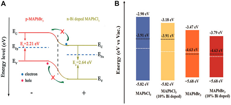
FIGURE 1. (A) Band structure of p-MAPbBr3/n-Bi doped MAPbCl3 heterosystem. (B) Energy level diagram of MAPbCl3, 10% Bi doped MAPbBr3, MAPbBr3 and 10% Bi doped p-MAPbBr3. Reproduced with permission from Ref. [23] (A, B).
Thus, as a promising methodology, doping reasonably can ensure the increase of carriers concentration and materials’ mobility, contributing to the reduction of dark current and the enhancement of sensitivity. In terms of future work, it has been suggested that two or more metal dopants, such as Cu, Mn, In, Ga and so on, could be applied simultaneously to compensate the partially doping impurity states [26] and tail the band.
2.2 Bandgap structure engineering with heterojunction
Recently, intrinsic monophase semiconductors without doping have been widely investigated. But intrinsic limitations of single material restrict the development of X-ray detection. To combine materials with various properties, heterojunciton has attracted much attention to be fabricated for detection performance enhancement [27, 28].
2.2.1 2D/3D perovskite heterojunction
3D perovskite continues to dominate the X-ray detector research attributed to its superior X-ray sensitivity. Unfortunately, the ion migration in 3D perovsite is especially distinct, particularly occurring on free surfaces and grain boundaries. The bonding of surface atoms is weak due to the breaking of chemical bonds [29]. In contrast, 2D perovskite with high resistance ensures the suppression of ion migration effectively and enlarges the energy barrier of hole injection without affecting carrier extraction. It would be a novel idea to grow 2D perovskite epitaxially on 3D perovskite to mitigate ion migration. However, the voids between 2D/3D perovskite heterojunction are the obstacles for long-term stability. Accordingly, organic spacer can be applied in filling voids of heterojunction to form compact interface, contributing to the increase of performance.
3D FAPbBr3 SC (single crystal) serves as a distinguished material for X-ray detection due to its high μτ product. But ion migration is the main downside at external bias, leading to severe dark current drift and device noise. Therefore, He et al. [19] utilized long-chain organic cation FPEA+ to separate octahedral sheet [PbBr6]4−, forming 2D epitaxial layer (FPEA)2PbBr4 on 3D FAPbBr3 SC surface tightly shown in Figure 2A. In contrast, 2D (FPEA)2PbBr4 SC can deactivate surface defects of 3D FAPbBr3 using wide gap detect deactivation effect. Through space-charge limited current (SCLC) technique, it was observed that the detect density (3.18 × 109cm−3) of heterojunction was decreased dramatically compared with FAPbBr3 (4.70 × 109cm−3). With the contrast of investigation of 3D/3D and 3D/2D’s photoluminescence (PL) spectra intensity after 5 min polarization, it was demonstrated that PL in 3D/3D film quenched severely while in 3D/2D film, however, few quench of PL intensity of 2D perovskite was obtained (Figures 2D,E). PL intensity of 3D perovskite also retains 80% of original value, proving that the ion migration was inhibited effectively. Meanwhile, the long-term job security was guaranteed. This technique enabled the biased heterojunciton had advanced performance in X-ray detecting application.
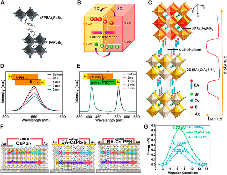
FIGURE 2. (A) The Schematic diagram of (FPEA)2PbBr4/FAPbBr3 heterojunction. (B) Band alignment and (C) schematic diagramof (BA)2CsAgBiBr7/Cs2AgBiBr6 heterocrystals. (D) (E) Photoluminescence (PL) spectra intensity of 3D FAPbBr3/3D FAPbBr3 and 3D FAPbBr3/2D (FPEA)2PbBr4 film. (F) Schematic presentation of CsPbI3, BA2CsPb2I7 and BA2CsPb2I7-CsPbI3 (BA-Cs PFH) planar heterojunction. (G) Simulated ion migration barriers of CsPbI3, BA2CsPb2I7 and BA2CsPb2I7-CsPbI3 (BA-Cs PFH) planar heterojunction. Reproduced with permission from Ref. [19] (A) (D) (E), Ref. [30] (B) (C), Ref. [31] (F) (G).
To modify the voids of 2D/3D heterojunction, Zhang et al. [30] regarded (BA)2CsAgBiBr7 as seed crystal, guiding its in situ epitaxial growth on 3D Cs2AgBiBr6 to form vertical type-II heterojunction (Figure 2B). With the decrease of temperature, nucleus expanded horizontally. Vertical inorganic [Ag(Bi)Br6]∞ layer was inhibited by large-volume BA+, separating the inorganic layers as shown in Figure 2C. New (BA)2CsAgBiBr7 crystals can fill voids inside heterojunction, forming sharp interface with intensive adhesion at atomic scale. 2D organic spacer was integrated with (BA)2CsAgBiBr7 to induce steric hindrance, increasing the activation energy to resist uncontrollable ion migration. Meanwhile, the formation of pn junction with Cs2AgBiBr6 as p-type and (BA)2CsAgBiBr7 as n-type yields the existence of built-in potential. Thus, X-ray generated carriers can be separated and transported effectively, and device noise can be also reduced, from which the heterojunction crystal can be driven by itself. The device can detect X-ray directly without external power supply, reducing dark current and dark current drift dramatically. The X-ray detector showed a low dark current of 3.2 × 10⁻² pA and a sensitivity of 206 μC Gyair−1 cm-2.
In other cases, Xu et al. [31] proposed the trade-off between BA2CsPb2I7 and 3D homologs CsPbI3. The authors designed asymmetrical plane film structure of BA2CsPb2I7-CsPbI3 perovskite film heterojunction (BA-Cs PFH) as shown in Figure 2F. For typical BA2CsPb2I7, ion migration can be suppressed to reduce dark current effectively due to quantum confinement effect and dielectric confinement of organic molecular layer (Figure 2G). Thus, the detector showed a high on-off ratio of ∼308 and detectivity of 0.092 μGyairs-1. Meanwhile, BA2CsPb2I7 minimized the leakage current. Considering the intrinsic defects and the capture and relief of ion migration in crystal lattice, it was demonstrated that BA-Cs PFH exhibited higher sensitivity than CsPbI3’s (<0.1s vs. ∼ 3 s).
Herein, the inhibited ion migration is prone to appear in 2D/3D structure which acts as the foundation for X-ray detector with high performance. And with the addition of organic molecular layer, halogen ion migration of inorganic halogen perovskite is suppressed. Notably, as the thickness of the organic molecular layer increases, the number of transferred electrons may decrease, so only a moderate value can be taken.
2.2.2 Device structure design
Detectors with novel structure, such as double layers heterostructure, p-i-n structure and so on, exhibit great potential for higher X-ray detection capability. Double heterostructure plays a dominant role in blocking carriers that generated inside the device structure [32], and only carriers that photogenerated within the top absorption layers can be completely depleted and collected, leading to a fast response [33]. With appropriate band direction design, double heterostructure can be obtained. Not only X-ray generated carriers transportation can be enhanced but also ion migration can be suppressed. Wei et al. [34] fabricated X-ray detector based on poly (3-hexylthiophene-2,5-diyl) (P3HT)/CsPbBr3 perovskite nanocrystals (PNCs)/(6,6)-Phenyl-C61 butyric acid methyl ester (PCBM) as two type-II heterostructures [Figure 3A]. Since the X-ray was sensitized, carriers generated by X-ray in PNCs can be separated and transported to P3HT and PCBM quickly due to the alignment of band structure [Figure 3B]. It was demonstrated that the sensitivity of P3HT:PCBM/CsPbBr3 hybrid device was increased by an order compared with P3HT:PCBM and CsPbBr3 devices. Sensitivity of double heterostructure exceeded two orders of magnitudes than PNC nano hybrid film due to self absorption effect, exhibiting its efficient detecting capability. Surrounding organic matrix can block the ion migration because it hindered the route of ion migration in organic net physically, ensuring higher electric field to enhance the efficiency of charge collection. This benefited the improvement of X-ray response and realization of low dark current drift (3.57 × 10⁻⁹cms-1V−1). Thus, the device showed a high X-ray generated current and low dark current, 30 times lower than PNC film 1.06 × 10⁻⁷ cm s-1V−1).
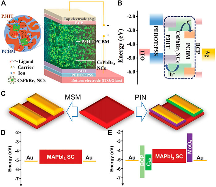
FIGURE 3. (A) Schematic diagram and (B) energy level of detector based on P3HT/PNCs/PCBM heterostructure. (C) Device structures of MSM and p-i-n; Energy level diagram of (D) MSM and (E) p-i-n device; Reproduced with permission from Ref. [34] (A,B, C), Ref. [36] (D, E).
It is shown in Figure 3C that p-i-n or metal-semiconductor-metal (MSM) structure photodetectors with high-speed and low-noise operation are widely employed in X-ray detector to enhance the sensitivity [35]. Accordingly, p-type and n-type charge transformation layers can be introduced to fabricate novel X-ray detector with p-i-n structure to reduce interface reaction and promote effective separation of carriers. This served a practical methodology to design devices with high responsivity and SNR. Song et al. [36] proposed X-ray detector based MAPbI3 SC. The charge transformation layer was inserted between MAPbI3 and Au to fabricate a MSM structure (Figure 3D). On the other hand, BCP/C60 and MoOx were applied in p-type and n-type carriers transportation layers, which were combined with MAPbI3 SC to form p-i-n structure as shown in Figure 3E. By comparing these two structures, it was found that the ion migration energy of p-i-n structure is higher than that of MSM structure (405 meV vs. 268meV). P-i-n structure displays excellent ion migration inhibition effect at reversed bias. At the same time, separating perovskite from electrode contact can reduce the polarity induced by elecrochemistry contributing to charge inhibition. As a result, the dark current of p-i-n device (∼1 nA) was lower three orders of magnitude compared with original condition. It made it possible to fabricate X-ray detector with high sensitivity (5.2 × 10⁶ μC Gyair−1 cm-2) and low detectivity (0.1 nGyair s-1).
For the above MSM structure, the time of carriers collection was excessively long under the reach-through bias. Even with a higher bias, the collection time still maintains long owing to the delay of carriers deep in semiconductor layer. More severely, thermionic emission and Schottky contact tunning are two main factors to increase the dark current. Hence, p-i-n has obvious superiority of quick response over MSM. Generally, introducing novel structure to X-ray detector is a promising way to optimize the performance of the detector, which can reduce the ion immigration and enhance the carriers transportation to increase the SNR.
2.2.3 Components modification
The gradient band distribution of low dimensional perovskite benefits the alignment of heterojunction band edges, facilitating the carriers transportation. As shown in Figure 4A, Xu et al. [37] proposed new formula through construction of two phases 2D (PEA)2MA3Pb4I13 (PEA = 2-phenylethylammonium, MA = methylammonium) and 3D MAPbI3 cascade. The contact of low dimensional (PEA)2MA3Pb4I13 and positive electrode fluorine-doped SnO2 (FTO) glass made VBM boundary deeper as shown in Figure 4D. Accordingly, amplified voids implantation energy decreased dark current, benefiting the enhancement of SNR. Although the slow response of X-ray can be mitigated by applying high electric field, the sensitivity of double layers perovskite detector based on effective holes circulation exhibited two orders of magnitude higher compared with 2D/3D and 2D/3D/2D sandwich structure as shown in Figures 4B,C.
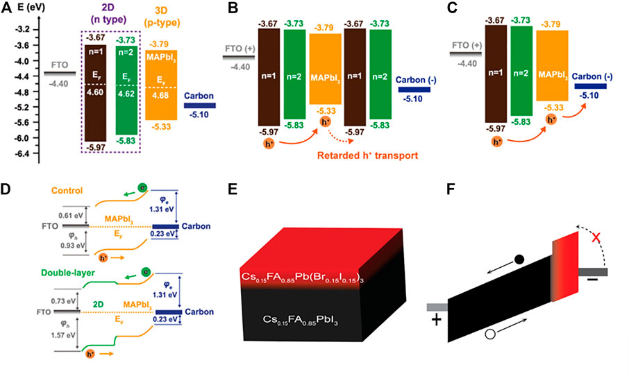
FIGURE 4. (A) Energy level diagram of 2D (PEA)2MA3Pb4I13 3D MAPbI3 heterosystem (n = 1,2 represent two phases of different annealing time). (B) Energy level diagram of 2D/3D/2D sandwich structure and (C) 2D/3D double layer structure. (D) Band alignment of 3D MAPbI3 single component device and 2D (PEA)2MA3Pb4I13/3D MAPbI3 device. (E) Schematic diagram and (F) band alignment of Cs0.15FA0.85Pb(I0.15Br0.85)3/Cs0.15FA0.85PbI3 heterojunction. Reproduced with permission from Ref. [37] (A) (B) (C) (D), Ref. [38] (E) (F).
In addition to construct cascade structure, introducing wide gap layer at the interface between perovskite and electrode can generate higher potential barrier, prohibiting the injection of holes or electrons to suppress dark current. Zhou et al. [38, 39]also reported Cs0.15FA0.85Pb(I0.15Br0.85)3/Cs0.15FA0.85PbI3 heterojunction adopting dip coating process (Figure 3E). The device can inhibit dark current under X-ray illumination at reversed bias. As shown in Figure 3F, perovskite with wide band gap Cs0.15FA0.85Pb(I0.15Br0.85)3 showed higher electrons injection barrier (∼1.0eV). Utilizing solar cell capacitance simulator, it turned out that calculated dark current density of heterojunction within WGB can be reduced to 0.73 ± 0.05 nA cm-2 due to the obstacle of electrons, which was two orders of magnitude lower than any single material at reversed bias.
Additionally, except the research about heterojunction based on perovskite such as p-MAPbBr3/n-CsPbBr3 [39], non-perovskite semiconductors can also provide abundant band structure candidates, including CuI [39], Te [40], etc. Although the above researches have been achieved, there still exist massive opportunities for future explore. The type-II heterojunction can be deemed as a reliable guideline of band structure design. On account of band alignment [41], the heterojunction promotes the separation of X-ray generated electrons/holes to realize higher detection performance. In terms of materials selection, it is worthwhile to exploit wide band gap materials to block carriers injection from the interface between the electrode and perovskite, even resulting in increase of trap density. And the other potential materials in this fields are ranging from organic material, inorganic salts, 2D materials and other related materials [42].
2.2.4 Interface modification
Organic molecules have been developed as electrons donor or acceptor, which can serve as middle layer for construction of dipoles to increase adhesion. Meanwhile, this dipole can modulate energy barriers and band alignment. As shown in Figure 5A, Wei et al. [28] applied brominated (3-aminopropyl) triethoxysilane molecule (APTES) as middle layer in MAPbBr3 integrated on Si device. Ammonium bromide group built up mechanical and electrical connection with MAPbBr3 crystals inherently. The shift of brominated APTES dipole’s vacuum level promoted the band alignment of Si and MAPbBr3, making a possibility of less rectification contact as shown in Figure 5B. This inserted APTES dipole layer exhibited high energy barrier for electrons injection and low energy barrier for holes extraction, leading to low dark current. The reduced dark current ensured the proper work of device at higher bias. Thus, the device exhibited a high sensitivity of 2.1 × 10⁴ μC Gyair−1 cm−2 under 8 keV X-ray radiation.
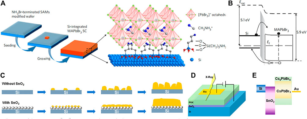
FIGURE 5. (A) Schematic diagram of fabrication of Si-integrated MAPbBr3 single crystal device. (B) Band interface alignment of MAPbBr3 and silicon. (C) Schematic illustration of perovskite chemical vapor deposition process with and without SnO2. (D) Device structure of SnO2/cesium-lead-bromide perovskite heterojunction and (E) energy level of the device. Reproduced with permission from Ref. [28] (A) (B), Ref. [29] (C) (D) (E).
Tons of sub-micro defects were distributed on both sides of perovskite, giving rise to interface voltage loss and the reduction of perovskite’s stability. To deactivate defects and promote charge transportation, inserting electron (SnO2, TiO2, ZnO) and hole (NiOx) transportation layer become necessary [43]. As shown in Figure 5C, Li et al. [30] inserted SnO2 nano layer between CsPbBr3 perovskite to form heterojunction. With the introduction of SnO2 nucleus, surface energy of system was reduced. In the meanwhile, perovskite prior deposition speed was significantly boosted, obtaining lower density defects and thicker film to suppress ion migration. Besides, due to the existence of electrons transportation layer, electron collection from perovskite layer to negative electrode can be enhanced, [Figure 5D, E] deriving X-ray detector with a high sensitivity of 2,930 μC Gyair−1 cm-2 and low detectivity of 120 nGyair s-1.
In other ways, polishing method like O3-UV treatment can be applied to passivate surface defects. Feng et al. [44] fabricated X-ray photodetector based on PEDOT:PSS/MAPbBr3/C60/BCP as shown in Figures 6A,B. PEDOT:PSS and C60/BCP serve as electron and hole transportation layers respectively to enhance charge generation. In this research, O3-UV treatment were applied on MAPbBr3 SC’s surface to passivate traps, leading to a drop of trap density from 2.59 × 1010cm-3 to 1.69 × 1010cm-3. Consequently, the detector with high photocurrent and low dark current was realized, as shown in Figure c d, which is consistent with low defect density.
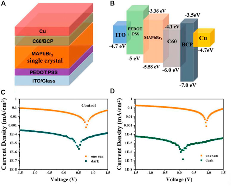
FIGURE 6. (A) Schematic diagram and (B) energy level of detector based on ITO/PEDOT: PSS/single crystals/C60/BCP/copper (Cu). (C) With and without O3-UV treated detector under dark and AM 1.5 illumination. Reproduced with permission from Ref. [44] (A) (B) (C) (D).
Essentially, both the insertion of SnO2 and the addition of small organic molecules are a means of defects passivation. They are regarded as modifiers of electrical properties, such as carrier mobility and work function. Foremost, more inorganic salts, small organic molecules and even other polymers deserves to be exploited for interface modification. And the approaches such as O3-UV treatment are value to utilize for passivating surface defects
3 Perovskite X-ray detectors with Electrode contact
Electrodes play an important role in improving performance of X-ray detectors. When selecting suitable electrodes, chemically stability and metal-semiconductor contact must be taken into consideration. For example, Al and Ag are more likely to react with halide perovskites compared to Au [36]. Besides, electrode contact technologies mainly used in perovskite X-ray detectors are Ohmic contacts and Schottky contacts. Ohmic contacts promote charge carrier transport. Detectors with Ohmic contacts usually work at low bias voltage, which means charge carriers are easily lost due to capture and recombination, and causes incomplete charge collection, resulting in poor energy resolution. To enhance charge collection, large bias is needed. However, it will cause the increased dark current. Compared to Ohmic detectors, Schottky detectors have higher Schottky barriers that create a built-in electric field, allowing them working as self-powered devices. Moreover, larger voltage can be applied because Schottky detectors work at reverse bias. Like a Schottky diode, when reverse bias is added, the depletion region extends and the leakage current level is low, thus promoting the charge collection and ensuring higher resolution [45].
3.1 Ohmic contacts
Ohmic contact promotes charge carrier transport. When Ohmic perovskite X-ray detectors work, an external bias was needed to drive ion migration. These symmetric devices have better performance at low bias voltage but present severe leakage (dark) current problems as the bias increases. For example, Au-perovskite-Au, a typical Ohmic contact structure, has been applied in recent researches. Chen et al. [46] have recorded electrical characteristics of the device with the structure of Au-(PEA)4AgInBr8 SCs-Au. They built a planar structure detector and made it exposed to X-ray with maximum energy of 50 keV, and a peak intensity of 30 keV. During the process (exposure dose rate: 34.5–138 μGy s−1), no rectification was found from Figure 7A, showing a good Ohmic contact between Au electrode and (PEA)4AgInBr8. They tested the sensitivity of the device at 20, 100 and 200 V mm−1, which was 21, 91 and 185 μC·Gyair−1 cm−1 (Figure 7B). Under electric field of 20 V mm-1, its dark current was 1.75 nA cm−2 and dark current drift was 7.33 × 10⁻⁷ nA cm-1.
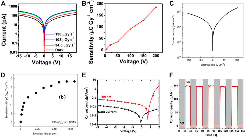
FIGURE 7. Photoelectric properties of perovskite X-ray detectors.(A) Dark (black) and response current−voltage (J−V) curves of the (PEA)4AgInBr8 SCs detector at dose rates of 34.5, 103, and 138 μGyair s −1. (B) Dependence of X-ray sensitivity on applied voltage based on (PEA)4AgInBr8 SCs detector. (C) Current density measurement under dark condition for an MAPbI3 wafer. The applied voltage ranges from −200 to +200 V, which corresponds to an electrical field of ±0.2 V μm-1. (D) Calculated sensitivity (S) of the X-ray responses in the RQA5 spectrum and a dose of 213 µGyair s−1. Optical response: (E) Current-voltage (IeV) curve of the devices under dark atmosphere and a wavelength of 405 nm laser. (F) Photoresponse of the device under 405 nm laser with the power density of 0.636 mW/cm2 at zero bias voltage. ON is the device under the exposure of laser. OFF is the device under a dark atmosphere. Reproduced with permission from Ref. [46] (A) (B), Ref. [50] (C) (D), Ref. [49] (E) (F).
Other examples like Au/Ag-Cs2AgBiBr6-Au/Ag also show some similar characteristics of ohmic detectors like relatively good sensitivity at low bias voltage and increase in dark current levels at high voltage. In Pan et al. [47]’s research, Cs2AgBiBr6 detector with Au electrodes showed dark current of ∼0.15 nA cm−2 at 5 V and sensitivity ranging from 8 to 105 µC Gyair−1 cm–2 (1 V–50 V bias). However, Dang et al. [48]’s work pointed out that the Ohmic contact behaviors between Au and Cs2AgBiBr6 are not perfect, resulting in obvious hysteretic I-V behaviors. Dang compared the energy level between Cs2AgBiBr6 single crystal and different metal electrodes including Au, Ag and Al, and constructed a better Ohmic contact of Ag with the Cs2AgBiBr6 SCs, which showed better photo-response and estimating detectivity (indicating the dark current level) of 1.38 × 10⁹ Jones in air.
Asymmetrical electrodes structures can also be applied in Ohmic detectors. According to Deumel et al. [49]’s work, the J-E plot (Figure 7C) showed typical Ohmic electrical behavior with the dark current density reaches the maximum value of 8.40 × 10⁻⁴ mA cm−2 for negative fields and 1.98 × 10⁻³ mA cm−2 for positive bias. This small difference may be attributed to asymmetrical electrodes and their different work functions (ϕm,Cr = 4.5 eV and ϕm,Pt = 5.7 eV). The maximum sensitivity of 9,300 μC·Gyair−1 cm−2 has been witnessed under the electrical field of 0.17 V μm−1, confirming the good sensitivity of Ohmic detectors with a low bias applied (Figure 7D).
3.2 Schottky contacts
In terms of perovskite X-ray detector, the high dark current level caused by 3D perovskites’ ion migration is one of the main obstacles that prevent it from practical application. One effective solution is to create asymmetrical electrode structures, forming Schottky barriers to suppress the severe ion migration problems. Recent researches about Schottky detectors have shown an enhancement in sensitivity and an decrease of dark current level at high bias voltage. Ag-perovskite-ITO sandwich structure is a commonly used strategy to create Schottky barriers for perovskite materials like MAPbBr3 or CsPbBr3. In work of Xu et al. [50], the Schottky contact at the interface of MAPbBr3/Ag has been formed, whose typical electrical characteristics are revealed by the current-voltage (I-V) (Figure 7E), curve and the high and stable On-Off I-V behavior (Figure 7F), making it easier for electrons to cross the barrier and be collected by Ag. Moreover, with the barrier created by ITO/MAPbBr3, a built-in electric field has been witnessed, promoting the photo-generated electron-hole pairs’ separation, thus showing significant improvement in the response performance of the detector. They also test the detector’s sensitivity with a bias voltage of 0 (35, 40, 45, 50 kV), which are 2.35 × 10⁻⁴, 2.02 × 10⁻⁴, 1.66 × 10⁻⁴ and 1.15 × 10⁻⁴ μC μGyair−1 cm–2,respectively. The dark current level can be demonstrated by the photoresponsivity (R), which is 22 mA/W in this case. Other Schottky X-ray detectors based on metal–perovskite-oxide semiconductor also exhibit high performances for X-ray detect. Xu et al. [51] replaced MAPbBr3 with CsPbBr3 to get a Schottky single crystal X-ray detector, which shows the Schottky behavior current−voltage (I−V) curve with the dark current density in the range of 5–25 nA/cm2 (Figure 8A). Different from Ohmic detector, this detector works at reverse voltage, with the sensitivity under inverse bias of −2, −4, −6, and −8 V are 172, 292, 475, and 770 μC Gy−1 cm−2, respectively (Figure 8C). Furthermore, under an X-ray dose rate of 333.69 μGy/s, the sensitivity at different reverse biases is in the range of 0.07–2.86 × 10³ μC·Gyair−1 cm−2 (Figure 8D). As shown in Figures 8A,B typical Schottky On-Off I-V behavior has been witnessed during the experiment.
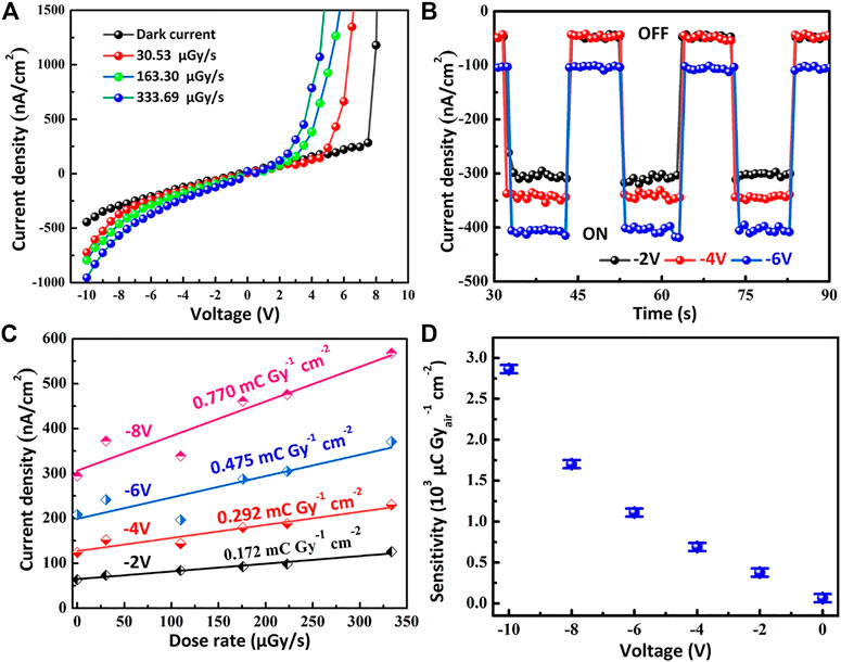
FIGURE 8. (A) I−V curve of CsPbBr3 SCs devices under various X-ray dose rates (30.53, 163.30, and 333.69 μGy/s). (B) On and off photocurrent density of CsPbBr3 SCs devices with different biases applied (−2, −4, and −6 V) and irradiated by a 45 keV X-ray. (C) Photocurrent response of CsPbBr3 SCs devices at different reverse biases under 40 keV X-ray various dose rates. (D) Sensitivity versus bias of CsPbBr3 SCs devices under a 45 keV X-ray at the dose rate of 333.69 μGy/s. Reproduced with permission from Ref. [51].
Other researches focus on metal electrode structure. Xu et al. [52] used Al and Au to create Schottky contact and Ohmic contact. From the relationship of the exposure X-ray dose rate and the current response.the sensitivity at 50, 100, 150, and 200 V is up to 109, 204, 271, and 359 μC Gy−1 cm−2. The response time is 76.2 ± 2.5 μs (200v, X-ray chopped at 2 kHz). The researchers later compare its electrical performance with an Ohmic detector with Au-MAPbBr3-Au (200 V bias, 50keV, 22.1 μGy/s, whose sensitivity and response time are 62 μC Gy−1 cm−2 and 272 ± 5 μs, confirming that Schottky detector’s sensitivity and response time are higher or faster than Ohmic detector. The better electrical performances are mainly attributed to the Schottky barrier between Al and MAPbBr3 SCs. This barrier could greatly suppress the leakage current at a high bias voltage, which allows higher electrical field (1.43 × 10⁷ V/m) than Ohmic detector, thus achieving higher sensitivity.
For CsPbBr3, He et al. [53] applied Bi-perovskite-Au structure. Bi was made positive while Au being negative, forming large Schottky barriers on both metal–semiconductor interface under reversed bias, which greatly simultaneously blocked the charges’ injection into the semiconductor and suppress the dark current level (on the order of 102 nA cm−2 at reverse bias voltage of 250 V cm−1). They then tested its sensitivity under various conditions (the X-ray tube voltage: 30–50 kV, the dose rate: 0.626 to 1.91 × 10⁴ μC·Gyair−1, which were in the range of few tens to over 8,000 μC·Gyair−1 cm−2. The high Schottky barriers also enabled the device’s self-powered X-ray detection with the sensitivity of ∼14 μC·Gyair−1 cm−2, which can be largely boosted to ∼192 μC·Gyair−1 cm−2 if 1 V reverse bias is applied.
4 Summary and perspective
Generally speaking, great strides have been achieved in perovskite-based X-ray detector. In this work, we have surveyed recent development of perovskite materials and devices for performance improvement of X-ray detector. There exists some representative examples where high sensitivity have been realized, and low limit detection have been reached. Concerning the materials modification, researchers mainly focus on interstitially doping, epitaxial wide band gap semiconductors, organic carriers transport layer to suppress dark current. We’re hopeful for upcoming researches that exploit more metal cationic dopants, polymers and other small organic molecules to modify the material. And the wide band gap semiconductor can be activated by narrow-band gap semiconductor to optimize the driving force of electron transport through quantum confinement effect. Hence, it is suggested to improve the detection performance. Furthermore, to design band structure of heterojunction, Type-II is expected for favorable charge separation, driving the perovskite-based X-ray detector to higher level. Whether organic material or inorganic salts are welcomed to be paired with perovskite, even 2D materials are desired to be employed. As for the device structure, the p-i-n device attributed to its high sensitivity, is superior to MSM one. Fortunately, the performance of MSM device can be improved through adopting double layer perovskite. Notably, based on the similarity, the materials and devices applied in photovoltaic field are valuable for reference.
Ohmic and Schottky contacts were also mainly investigated for electrode-perovskite contacts in recent studies. In these researches, Ohmic contact enables great stability but high dark current while Schottky contact demands higher voltage bias but shows the ability of dark current suppression. Metal materials, device structure and energy level should be considered for desired properties of carrier transportation. At same time, more efforts should be paid to dig in-depth mechanisms of electrodes interface to understand more clearly.
In summary, further researches are expected to enhance the sensitivity and response speed while decreasing the limit of detection. And proper material band and device structure design will lay foundation for commercial and large-scale perovskite X-ray detector.
Author contributions
YH summarized the papers and wrote the introduction and band theory. ZW wrote band engineering with heterojunction and summary. ZW wrote perovskite X-ray detectors with Electrode contact. All authors discussed the results and commented on the manuscript.
Funding
This work was supported by Beijing Natural Science Foundation (M22020), the National Key R&D Program (2020YFA0709800) and National Natural Science Foundation (U20A20168, 51861145202, 61874065, 62022047) of China. HT is grateful for the support of Fok YingTong Education Foundation (Grant No. 171051), Beijing National Research Center for Information Science and Technology Youth Innovation Fund (BNR2021RC01007), State Key Laboratory of New Ceramic and Fine Processing Tsinghua University (No. KF202109), and Tsinghua-Foshan Innovation Special Fund (TFISF) (2021THFS0217).
Conflict of interest
The authors declare that the research was conducted in the absence of any commercial or financial relationships that could be construed as a potential conflict of interest.
Publisher’s note
All claims expressed in this article are solely those of the authors and do not necessarily represent those of their affiliated organizations, or those of the publisher, the editors and the reviewers. Any product that may be evaluated in this article, or claim that may be made by its manufacturer, is not guaranteed or endorsed by the publisher.
References
1. Kasap SO, Rowlands JA. Direct-conversion flat-panel X-ray image sensors for digital radiography. Proc Ieee (2002) 90(4):591–604. doi:10.1109/jproc.2002.1002529
2. Wei HT, Huang JS. Halide lead perovskites for ionizing radiation detection. Nat Commun (2019) 10:1066. doi:10.1038/s41467-019-08981-w
3. Chen QS, Wu J, Ou X, Huang B, Almutlaq J, Zhumekenov AA, et al. All-inorganic perovskite nanocrystal scintillators. Nature (2018) 561(7721):88–93. doi:10.1038/s41586-018-0451-1
4. Zhou Y, Chen J, Bakr OM, Mohammed OF. Metal halide perovskites for X-ray imaging scintillators and detectors. Acs Energ Lett (2021) 6(2):739–68. doi:10.1021/acsenergylett.0c02430
5. Xia M, Yuan J, Niu G, Du X, Yin L, Pan W, et al. Unveiling the structural descriptor of AX9 perovskite derivatives toward X-ray detectors with low detection limit and high stability. Adv Funct Mater (2020) 30(24):1910648. doi:10.1002/adfm.201910648
6. Wangyang PH, Gong C, Rao G, Hu K, Wang X, Yan C, et al. Recent advances in halide perovskite photodetectors based on different dimensional materials. Adv Opt Mater (2018) 6(11):1701302. doi:10.1002/adom.201701302
7. Sun SB, Yuan D, Xu Y, Wang A, Deng Z. Ligand-mediated synthesis of shape-controlled cesium lead halide perovskite nanocrystals via reprecipitation process at room temperature. Acs Nano (2016) 10(3):3648–57. doi:10.1021/acsnano.5b08193
8. Zhao W, Rowlands JA. X-ray imaging using amorphous selenium: Feasibility of a flat panel self-scanned detector for digital radiology. Med Phys (1995) 22(10):1595–604. doi:10.1118/1.597628
9. Kasap SO. X-Ray sensitivity of photoconductors: Application to stabilized a-Se. J Phys D-Applied Phys (2000) 33(21):2853–65. doi:10.1088/0022-3727/33/21/326
10. Keshavarz M, Debroye E, Ottesen M, Martin C, Zhang H, Fron E, et al. Tuning the structural and optoelectronic properties of Cs2AgBiBr6 double-perovskite single crystals through alkali-metal substitution. Adv Mater (2020) 32(40):2001878. doi:10.1002/adma.202001878
11. Yan J, Gao F, Tian Y, Li Y, Gong W, Wang S, et al. Controllable perovskite single crystal heterojunction for stable self-powered photo-imaging and X-ray detection. Adv Opt Mater (2022) 10(17):2200449. doi:10.1002/adom.202200449
12. Yakunin S, Dirin DN, Shynkarenko Y, Morad V, Cherniukh I, Nazarenko O, et al. Detection of gamma photons using solution-grown single crystals of hybrid lead halide perovskites. Nat Photon (2016) 10(9):585–9. doi:10.1038/nphoton.2016.139
13. Yang B, Pan W, Wu H, Niu G, Yuan JH, Xue KH, et al. Heteroepitaxial passivation of Cs2AgBiBr6 wafers with suppressed ionic migration for X-ray imaging. Nat Commun (2019) 10(1):1989–10. doi:10.1038/s41467-019-09968-3
14. Yan KR, Chen J, Ju H, Ding F, Chen H, Li CZ. Achieving high-performance thick-film perovskite solar cells with electron transporting Bingel fullerenes. J Mater Chem A (2018) 6(32):15495–503. doi:10.1039/c8ta05636f
15. He X, Xia M, Wu H, Du X, Song Z, Zhao S, et al. Quasi-2D perovskite thick film for X-ray detection with low detection limit. Adv Funct Mater (2022) 32(7):2109458. doi:10.1002/adfm.202109458
16. Zhuang RZ, Wang X, Ma W, Wu Y, Chen X, Tang L, et al. Highly sensitive X-ray detector made of layered perovskite-like (NH4)(3)Bi2I9 single crystal with anisotropic response. Nat Photon (2019) 13(9):602–8. doi:10.1038/s41566-019-0466-7
17. Zhang JY, Li A, Li B, Yang M, Hao X, Wu L, et al. Top-seed solution-based growth of perovskite Cs3Bi2I9 single crystal for high performance X-ray detection. Acs Photon (2022) 9(2):641–51. doi:10.1021/acsphotonics.1c01647
18. Yin WJ, Shi TT, Yan YF. Unusual defect physics in CH3NH3PbI3 perovskite solar cell absorber. Appl Phys Lett (2014) 104(6):063903. doi:10.1063/1.4864778
19. He YH, Pan W, Guo C, Zhang H, Wei H, Yang B. 3D/2D perovskite single crystals heterojunction for suppressed ions migration in hard X-ray detection. Adv Funct Mater (2021) 31(49):2104880. doi:10.1002/adfm.202104880
20. Karl N. Charge carrier transport in organic semiconductors. Synth Met (2003) 133:649–57. doi:10.1016/s0379-6779(02)00398-3
21. Hu ZS, Lin Z, Su J, Zhang J, Chang J, Hao Y. A review on energy band-gap engineering for perovskite photovoltaics. Solar Rrl (2019) 3(12):1970116. doi:10.1002/solr.201970116
22. Xie JS, Hang P, Wang H, Zhao S, Li G, Fang Y, et al. Perovskite bifunctional device with improved electroluminescent and photovoltaic performance through interfacial energy-band engineering. Adv Mater (2019) 31(33):1902543. doi:10.1002/adma.201902543
23. Pan Y, Wang X, Zhao J, Xu Y, Li Y, Li Q, et al. Photodiodes based on a MAPbBr 3/Bi 3+-doped MAPbCl 3 single crystals heterojunction for the X-ray detection. CrystEngComm (2021) 23(28):4954–62. doi:10.1039/d1ce00406a
24. Ulatowski AM, Wright AD, Wenger B, Buizza LRV, Motti SG, Eggimann HJ, et al. Charge-carrier trapping dynamics in bismuth-doped thin films of MAPbBr(3) perovskite. J Phys Chem Lett (2020) 11(9):3681–8. doi:10.1021/acs.jpclett.0c01048
25. Yamada Y, Hoyano M, Akashi R, Oto K, Kanemitsu Y. Impact of chemical doping on optical responses in bismuth-doped CH3NH3PbBr3 single crystals: Carrier lifetime and photon recycling. J Phys Chem Lett (2017) 8(23):5798–803. doi:10.1021/acs.jpclett.7b02508
26. Kamat PV. Semiconductor nanocrystals: To dope or not to dope. J Phys Chem Lett (2011) 2(21):2832–3. doi:10.1021/jz201345y
27. Zheng Z, Zu X, Zhang Y, Zhou W. Rational design of type-II nano-heterojunctions for nanoscale optoelectronics. Mater Today Phys (2020) 15:100262. doi:10.1016/j.mtphys.2020.100262
28. Wei W, Zhang Y, Xu Q, Wei H, Fang Y, Wang Q, et al. Monolithic integration of hybrid perovskite single crystals with heterogenous substrate for highly sensitive X-ray imaging. Nat Photon (2017) 11(5):315–21. doi:10.1038/nphoton.2017.43
29. Li LQ, Fang YJ, Yang DR. Interlayer-assisted growth of Si-based all-inorganic perovskite films via chemical vapor deposition for sensitive and stable X-ray detection. J Phys Chem Lett (2022) 13(24):5441–50. doi:10.1021/acs.jpclett.2c01389
30. Zhang XY, Zhu T, Ji C, Yao Y, Luo J. In situ epitaxial growth of centimeter-sized lead-free (BA)(2)CsAgBiBr7/Cs2AgBiBr6 heterocrystals for self-driven X-ray detection. J Am Chem Soc (2021) 143(49):20802–10. doi:10.1021/jacs.1c08959
31. Xu YK, Li Y, Peng G, Wang Q, Li Z, Wang H, et al. Asymmetric metal halide film with suppressed leakage current for high sensitive X-ray detection and imaging. Ieee Electron Device Lett (2022) 43(10):1709–12. doi:10.1109/led.2022.3202173
32. Kim J, Johnson W, Kanakaraju S, Lee CH. Lateral InP/InGaAs double heterojunction phototransistor over a trenched interdigitated finger structure. Solid-State Elect (2007) 51(7):1023–8. doi:10.1016/j.sse.2007.05.010
33. Brennan KF, Haralson J, Parks JW, Salem A. Review of reliability issues of metal-semiconductor-metal and avalanche photodiode photonic detectors. Microelectronics Reliability (1999) 39(12):1873–83. doi:10.1016/s0026-2714(99)00197-3
34. Wei JJ, Tao L, Li L, Yan M, Wang C, Sun W, et al. Tuning the photon sensitization mechanism in metal-halide-perovskite-based nanocomposite films toward highly efficient and stable X-ray detection. Adv Opt Mater (2022) 10(7):2102320. doi:10.1002/adom.202102320
35. Wang JH, Fu S, Huang L, Lu Y, Liu X, Zhang J, et al. Heterojunction engineering and ideal factor optimization toward efficient MINP perovskite solar cells. Adv Energ Mater (2021) 11(48):2102724. doi:10.1002/aenm.202102724
36. Song YL, Li L, Hao M, Bi W, Wang A, Kang Y, et al. Elimination of interfacial-electrochemical-reaction-induced polarization in perovskite single crystals for ultrasensitive and stable X-ray detector arrays. Adv Mater (2021) 33(52):2103078. doi:10.1002/adma.202103078
37. Xu XW, Qian W, Wang J, Yang J, Chen J, Xiao S, et al. Sequential growth of 2D/3D double-layer perovskite films with superior X-ray detection performance. Adv Sci (2021) 8(21):2102730. doi:10.1002/advs.202102730
38. Zhou Y, Zhao L, Ni Z, Xu S, Zhao J, Xiao X, et al. Heterojunction structures for reduced noise in large-area and sensitive perovskite x-ray detectors. Sci Adv (2021) 7(36):eabg6716. doi:10.1126/sciadv.abg6716
39. Cui F, Zhang P, Zhang L, Hua Y, Sun X, Li X, et al. Liquid-phase epitaxial growth of large-area MAPbBr3–nCln/CsPbBr3 perovskite single-crystal heterojunction for enhancing sensitivity and stability of X-ray detector. Chem Mater (2022) 34(21):9601–12. doi:10.1021/acs.chemmater.2c02266
40. Dun GH. Cs2AgBiBr6 -Tellurium heterojunction-based high-performance X-ray detectors. In: 6th IEEE Electron Devices Technology and Manufacturing Conference (EDTM). Electr Network (2022).
41. Kaushik S, Naik TR, Alka A, Garg M, Tak BR, Ravikanth M, et al. Surface modification of AlN using organic molecular layer for improved deep UV photodetector performance. Acs Appl Electron Mater (2020) 2(3):739–46. doi:10.1021/acsaelm.9b00811
42. Franciosi A, Van de Walle CG. Heterojunction band offset engineering. Surf Sci Rep (1996) 25(1-4):1–140. doi:10.1016/0167-5729(95)00008-9
43. Gao ZW, Wang Y, Choy WCH. Buried interface modification in perovskite solar cells: A materials perspective. Adv Energ Mater (2022) 12(20):2104030. doi:10.1002/aenm.202104030
44. Feng A, Xie S, Fu X, Chen Z, Zhu W. Inch-sized thin metal halide perovskite single-crystal wafers for sensitive X-ray detection. Front Chem (2022) 9:823868. doi:10.3389/fchem.2021.823868
45. Gnatyuk V, Maslyanchuk O, Solovan M, Brus V, Aoki T. CdTe X/γ-ray detectors with different contact materials. Sensors (2021) 21(10):3518. doi:10.3390/s21103518
46. Chen D, Niu G, Hao S, Fan L, Zhao J, Wolverton C, et al. Decreasing structural dimensionality of double perovskites for phase stabilization toward efficient X-ray detection. ACS Appl Mater Inter (2021) 13(51):61447–53. doi:10.1021/acsami.1c20234
47. Pan WC, Wu H, Luo J, Deng Z, Ge C, Chen C, et al. Cs2AgBiBr6 single-crystal X-ray detectors with a low detection limit. Nat Photon (2017) 11(11):726–32. doi:10.1038/s41566-017-0012-4
48. Dang YY, Tong G, Song W, Liu Z, Qiu L, Ono LK, et al. Interface engineering strategies towards Cs2AgBiBr6 single-crystalline photodetectors with good Ohmic contact behaviours. J Mater Chem C (2020) 8(1):276–84. doi:10.1039/c9tc04780h
49. Deumel S, van Breemen A, Gelinck G, Peeters B, Maas J, Verbeek R, et al. High-sensitivity high-resolution X-ray imaging with soft-sintered metal halide perovskites. Nat Elect (2021) 4(9):681–8. doi:10.1038/s41928-021-00644-3
50. Xu Q, Zhang B, Nie J, Zhang H, Ouyang X, Liu J, et al. Self-powered X-ray detector based on methylammonium lead tribromide single crystals. J Alloys Comp (2021) 859:157826. doi:10.1016/j.jallcom.2020.157826
51. Xu Q, Wang X, Zhang H, Shao W, Nie J, Guo Y, et al. CsPbBr3 single crystal X-ray detector with Schottky barrier for X-ray imaging application. Acs Appl Electron Mater (2020) 2(4):879–84. doi:10.1021/acsaelm.9b00832
52. Xu Q, Shao W, Li Y, Zhang X, Ouyang X, Liu J, et al. High-performance surface barrier X-ray detector based on methylammonium lead tribromide single crystals. Acs Appl Mater Inter (2019) 11(10):9679–84. doi:10.1021/acsami.8b21605
Keywords: perovskite, band engineering, x-ray detector, heterojunction, electrode contact
Citation: He Y, Wang Z, Wang Z, Dun G-H, Geng X, Wang C, Du J, Guo T, Xie D, Tian H, Yang Y and Ren T-L (2023) Perovskite band engineering for high-performance X-ray detection. Front. Phys. 11:1114242. doi: 10.3389/fphy.2023.1114242
Received: 02 December 2022; Accepted: 23 March 2023;
Published: 05 April 2023.
Edited by:
Ge Yang, North Carolina State University, United StatesReviewed by:
Jafar Iqbal Khan, Northwestern University, United StatesZhaolai Chen, Shandong University, China
Copyright © 2023 He, Wang, Wang, Dun, Geng, Wang, Du, Guo, Xie, Tian, Yang and Ren. This is an open-access article distributed under the terms of the Creative Commons Attribution License (CC BY). The use, distribution or reproduction in other forums is permitted, provided the original author(s) and the copyright owner(s) are credited and that the original publication in this journal is cited, in accordance with accepted academic practice. No use, distribution or reproduction is permitted which does not comply with these terms.
*Correspondence: Dan Xie, eGllZGFuQHRzaW5naHVhLmVkdS5jbg==; He Tian, dGlhbmhlODhAdHNpbmdodWEuZWR1LmNu; Yi Yang, eWl5YW5nQHRzaW5naHVhLmVkdS5jbg==; Tian-Ling Ren, UmVuVExAdHNpbmdodWEuZWR1LmNu
†These authors have contributed equally to this work