 Ziqing Li
 Changcai Cui
 Xiaolong Zhou4
 Subiao Bian
 Oriol Arteaga
- 1Institute of Manufacturing Engineering, Huaqiao University, Xiamen, China
- 2National and Local Joint Engineering Research Center for Intelligent Manufacturing Technology of Brittle Material Products, Huaqiao University, Xiamen, China
- 3Department de Física Aplicada, Feman Group, Universitat de Barcelona, Barcelona, Spain
- 4Functional Thin Films Research Center, Shenzhen Institute of Advanced Technology, Chinese Academy of Sciences, Shenzhen, China
- 5Institute of Nanoscience and Nanotechnology (IN2UB), Universitat de Barcelona, Barcelona, Spain
In this work, a series of amorphous carbon films were deposited on a-plane sapphire substrates by magnetron sputtering with deposition time from 15 min to 8 h, in order to investigate the thickness and optical properties in the process of growth in a non-destructive way. They were characterized by using Mueller matrix spectroscopic ellipsometry together with topography profilometry and Raman spectroscopy. Two models of a Bruggeman effective medium approximation model and a single Cody-Lorentz oscillator model have been proposed to fit films thickness and optical constants from Ultraviolet (UV) to visible (210 nm–800 nm), and Transmission Electron Microscope (TEM) has been used to verify the proposed model for thickness fitting results. The optical constants of the amorphous carbon film have been determined by fitting together all measurements in samples deposited for 2 h or more, with the film thickness being the only sample-independent parameter. The results show that the thickness from 5 nm to 200 nm can be characterized in a nondestructive way although there is a relatively large thickness error compared with the Transmission Electron Microscope results for thin films (d < 20 nm) when the deposition time is less than 2 h because of the nonuniform deposition in the beginning. The relative error between the TEM and Spectroscopic Ellipsometry results can be reduced to 1% after 4 h sample. That means spectroscopic ellipsometry can still provide an indicator for the trend of thickness growth.
1 Introduction
Amorphous carbon films have outstanding mechanical, optical and chemical properties [1–3] and they have several applications as a surface coatings for industrial products, antireflective coatings etc [4–6]. Due to their high transmittance in infrared and microwave bands, they have also important applications for energy storage in solar cells or as field emitters and infrared window materials [7,8]. The deposition of amorphous carbon films on sapphire substrates combines the advantageous properties of the substrate and the film, which include good optical transparency, very high hardness and chemical inertness. Their applications include corrosion and radiation-resistant infrared windows, solid-state lasers and novel scanning probe microscopy applications [9,10]. Amorphous carbon, also known as Diamond-Like Carbon (DLC), is a meta-stable material composed of sp2 and sp3 hybrid bonds, which has the excellent characteristics of diamond and graphite. A variety of bonding forms makes amorphous carbon films show different optical and electronic properties [11,12]. The process of growth, the thickness uniformity and optical properties of the film will directly affect its application and service life. Therefore, the characterization of the thickness and optical properties of DLC films is of practical significance to better understand its mechanical and optical applications.
In this work, the thickness and optical properties of amorphous carbon films on sapphire substrate are characterized by Mueller Matrix Spectroscopic Ellipsometry (MMSE), and topographic profilometry and Raman spectroscopy were used to assist the ellipsometry analysis. Raman spectroscopy can characterize the relative content of sp2 and sp3 in diamond-like carbon films. It can be also used to study the valence bond type of films and assist in the analysis of film quality [13]. Various other techniques can be also used to study the thin film surface quality: Atomic Force Microscopy (AFM), Scanning Electron Microscopy (SEM) and optical microscopy and white light interferometry [14,15].
SE characterization is the main focus of this work. SE works by measuring the change of polarization state of reflected light on the film surface. Empirical knowledge is used to establish an appropriate optical model which is employed to fit the measured spectra in to obtain the optical constants and/or the thickness of the film [16]. Mori et al. used SE to characterize ion-deposited DLC films, and measured the film thickness (about 600 nm) and the optical properties of DLC in the wavelength range of 300–850 nm [17]. Hiratsuka et al. proposed a method to distinguish the types of DLC films by using optical properties such as refractive index and extinction coefficient. Four different types of DLC films, with thicknesses of more than 500 nm, were prepared with different experimental deposition methods and compared with their optical constants [18]. Zhou et al. established the relationship between SE and near-edge X-ray absorption fine-structure by depositing different types of diamond-like carbon films. The film thickness they considered was between 66 nm and 500 nm [19]. In a different work, they also conducted a more in-depth study on the optical models of DLC films for SE [20]. They deposited and prepared 13 different types of diamond-like films, established 10 optical models based on experience and existing knowledge, and verified their feasibility, where the thickness ranges from 26 to 300 nm. Domantas et al. have investigated the effect of Al doping on the refractive index and extinction coefficient of hydrogen-free and hydrogenated DLC films with film thicknesses of 39 nm–47 nm and 84 nm–162 nm, respectively [21]. Yang et al. have investigated the morphology, structure and optical properties of DLC films synthesized under different conditions. And thicknesses from 39 nm to 144 nm are grown on the surface of crystalline silicon, and its photovoltaic conversion Solar cells vary in efficiency[22]. All these previous results, show that a wide variety of optical models for different DLC films have been proposed and analyzed, but the initial process of growth until a uniform film thickness is achieved is less well documented by SE.
This paper studies the evolution of thickness and optical properties of amorphous carbon films deposited on the sapphire substrates with varying deposition time, aiming to characterize the evolution with a non-destructive way, and define the critical conditions that warrant an uniform film deposition on sapphire substrates. The film thickness evolution and the refractive indices are analyzed and discussed for films with thicknesses ranging from ∼5 nm to ∼ 200 nm, and a simple model for the DLC film based on one single oscillator is proposed. The results show that when the thickness reaches a certain critical value, the surface roughness remains almost unchanged. These results will be interesting for mechanical and optical applications combining sapphire substrates with DLC films.
2 Experiments
2.1 Sample preparation
The substrate was chosen to be single-crystal sapphire. Sapphire is a transparent and weakly optically anisotropic material widely used in photoelectric applications. The sapphire substrates were cut into 10 mm × 10 mm plates, and the crystal orientation is A plane
Nine amorphous carbon film samples with different thicknesses have been grown on sapphire substrates by magnetron sputtering. A carbon target (99.95% in purity) with a diameter of 50 mm was used for sputtering and the distance of the target to the substrate was 150 mm. Before deposition, the vacuum chamber was firstly pumped to the pressure of 5×10⁻³ Pa. The gas flow rate of Ar was set at 30.0 sccm, and the substrate holder rotated at a constant speed of 1 r min−1 during the film depositing. Besides, the sputtering power was kept at 30 W, bias voltage was maintained at 50 V, deposition time was 0.25–8 h, and a mass flow controller was applied to monitor the flow rates of Ar (99.99%). The sapphire substrates were cleaned with acetone and anhydrous ethanol several times in sequence and dried at 80 °C or 15 min. The amorphous carbon films with different film thicknesses, with varying deposition time of 15 min, 1 h, 2 h, 3 h, 4 h, 5 h, 6 h, 7 h and 8 h were obtained.
2.2 Characterization methods
The thickness and optical properties of amorphous carbon films were investigated in the 210–800 nm range under the incident angle of 70°, by using a Mueller matrix ellipsometer using four photoelastic modulators (4-PEMs) of different frequency, which precision is better than 0.001 [24]. The full Mueller matrix of all samples are measured by this instrument. The surface roughness of each amorphous carbon film was observed by the 3D profilometer (New View 7300, Zygo), in which the vertical and horizontal resolutions are 0.1 nm and 0.11 μm, respectively. Under this horizontal resolution, the field of view is 50 μm × 70 μm. It can analyze the film deposition quality and uniformity. The composition of film was measured by scanning probe micro Raman system (Alpha 300ra, WiTEC), which can effectively characterize the composition changes of the amorphous carbon film through Raman spectrum characteristics. This will provide the information that DLC film has been deposited on the substrate for ellipsometry analysis. Transmission electron microscopy (JEM-2100F) was used to characterize the film thickness. Cross-section TEM samples were prepared by a focused ion beam in parallel to the edge of the substrate directions and diluted to about 50 nm. This analysis can be used to verify the accuracy of ellipsometry fitting.
3 Results and discussion
3.1 Surface morphology and composition analysis
In order to characterize the film deposition quality and uniformity, the surface of the samples was divided into 9 portions for the profilometry analysis as it is shown in Figure 1. Panels 1A and 1C show the surface roughness of the film deposited for 15 min and deposited for 2 h is more flat than 1 h sample. When the film is deposited for 2 h, its uniformity is better than that of 1 h, as shown in Figure 1B, the film deposited for 1 h seems rougher than others. It can be seen that the surface uniformity of the film is improved with the increase of deposition time, as for short deposition time the film is discontinuous. As the film thickness reaches the critical thickness, that be estimated at around 2 h, the film surface seems to be continuous, which means the substrate is covered at all places by the film.
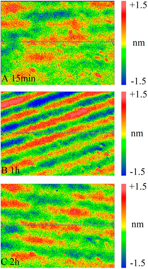
FIGURE 1. Surface roughness of films at different growth time (Sa: nm) (A)for 15 min sample, (B) for 1 h sample and (C) for 2 h sample.
The values of surface roughness Sa shown in Figure 2 are the average values of 9 areas. The surface roughness Sa of the bare sapphire substrates were less than 0.3 nm, and after DLC deposition the roughness remains low. Its small increase can be due to the fact that as there is no buffer layer between the substrate and the film, the surface of the substrate needs to become slightly more rough before the film can be deposited.
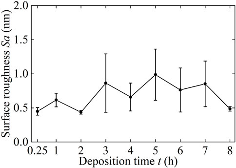
FIGURE 2. Surface roughness Sa of DLC films with deposition time.
Raman spectroscopy is a common method used to analyze the structure of amorphous carbon, and it is one of the most effective means to characterize the bond states of sp2 and sp3. As shown in Figure 3, the sapphire substrate mainly has 5 characteristic peaks, 378 cm−1, 417 cm−1, 576 cm−1, 644 cm−1 and 747 cm−1 [25,26].
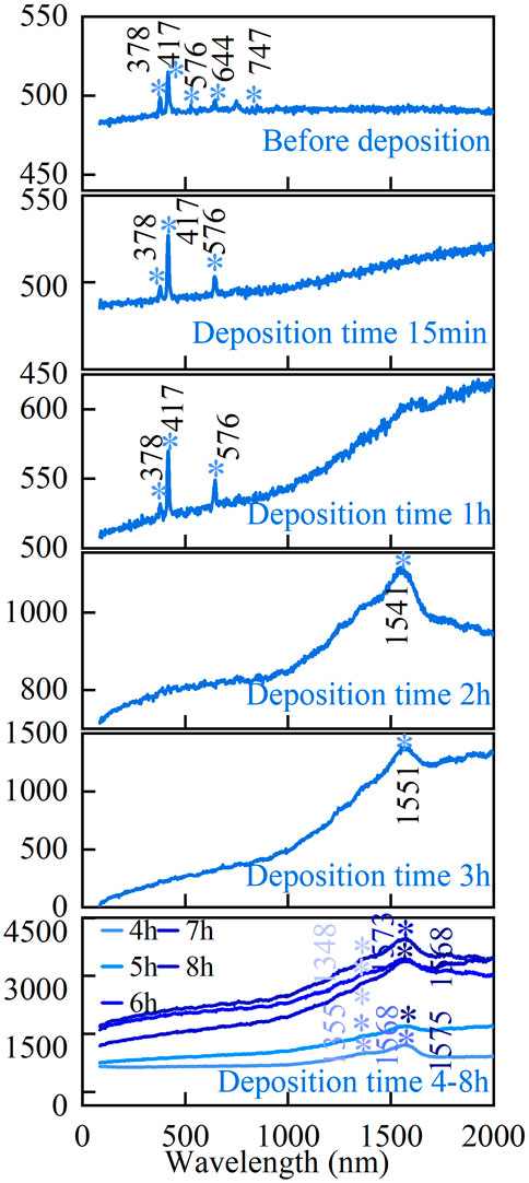
FIGURE 3. Raman spectra of amorphous carbon films with different deposition time.
As the film deposition time increases, the characteristic peaks of sapphire are gradually covered. When the deposition time is about 15 min, the two characteristic peaks of sapphire at 576 cm−1 and 747 cm−1 are covered. Due to the thin thickness of DLC film, the sapphire peak comes from the sapphire substrate and also can be found. After 1 h of film deposition, the three obvious characteristic peaks of 378 cm−1, 417 cm−1 and 644 cm−1 are still visible, and there are no other clear characteristic peaks, but the Raman intensity increases significantly after 1000 cm−1. The entire curve has a clear upward trend. After 4 h of deposition, obvious peaks appeared near 1350 cm−1 and 1580 cm−1, indicating that the structure of the amorphous carbon film had appeared at this time. Because the characteristic peak of 1580 cm−1 shifts to the low-frequency direction, it indicates that the sp3 bond with distortion in the film is reduced, and the sp2 bond density is higher. As shown in Figure 3, the characteristic peak of 1580cm−1 moves the fastest in the direction of low-frequency at 4 h, indicating that within this range, the sp2 bond density content in the film is the highest.
3.2 SE analysis
The spectroscopic Mueller matrix of all the samples were measured at an angle of incidence of 70°. Despite the sapphire substrate already had a roughened backside, a piece of scattering scotch tape was used in the backside to further ensure that backside reflections from the transparent substrate were avoided. No appreciable depolarization was observed in any of the measurements. Depolarization at noise level was treated during the first step of data analysis which consisted of getting the closest non-depolarizing estimate to each measured Mueller matrix. This step can be routinely done with Cloude decomposition [27], so that the measured Mueller matrix can be expressed in terms of Jones matrix. When normalized, the first element of this Jones matrix provides the complex reflection ratio ρ for p and s polarizations that is used to define the usual ellipsometry angles, Ψ and Δ, as
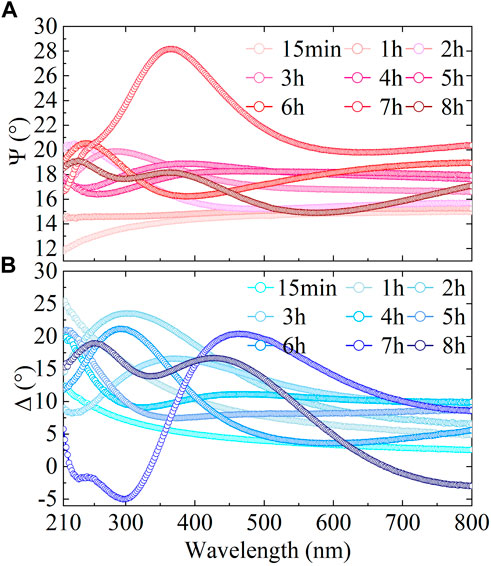
FIGURE 4. Ellipsometry data of DLC films with deposition time. (A) Ψ spectra of DLC films (B) Δ spectra of DLC films.
The increasing thickness of the DLC films with the deposition time is denoted by the clear evolution of the Ψ and Δ in Figure 4. The off-diagonal elements of the normalized Jones matrix, ρps and ρsp had vanishing values within the experimental accuray of our mesaurements. All samples were analyzed with the same optical model consisting of a multilayer form by roughness layer/amorphous carbon layer/sapphire substrate. The surface roughness layer was described by a Bruggeman Effective Medium Approximation (EMA) composed of 50% air and 50% amorphous carbon, unlike the surface roughness Sa, is just an equivalent model. The amorphous carbon layer is described by a single Cody-Lorentz oscillator, which is parameterized as [28]:
where E is the photon energy, AUV is the UV amplitude, EUV is the energy of the UV pole, ACL defines the amplitude (unitless) of the oscillator, BCL is a broadening term, Eo is the peak transition energy, Ep is the transition energy between the absorption onset and the Lorentzian oscillator and E1 = EtG (Et)L (Et). G (Et) is the near-bandgap function that defines the Cody behavior of the oscillator, L (Et) is the Lorentz oscillator function for the Lorentz behavior of the oscillator. The functions of G (Et) and L (Et) can be found in [29]. The transparent sapphire substrate is described by a Cauchy dispersion equation with two parameters A and B:
The Cauchy parameters used are A = 1.757, B = 0.0055 nm2, which were obtained from a fit on bare sapphire substrates during another work [30].
Good agreement was achieved between the measured data and fitted curves for all samples except for those with deposition time of 15 min and 1 h. These two samples will be later discussed in more detail. All remaining measurements (corresponding to deposition time of 2 h, 3 h, 4 h, 5 h, 6 h, 7 h and 8 h) were fit together with this model, ensuring that the same optical constants were used to describe the DLC films. The only individual fit parameters for each sample were the thickness of the DLC film and the thickness of the roughness overlayer.
The simulation results of the films deposited for more than 2 h samples are shown in Figure 5. The solid lines represent the experimental data and the dashed lines the fitted data in the optical model. All samples within these deposition time have a good fit to the same model. The Cody-Lorentz parameters used to model the optical constants of the DLC films are shown in Table 1, while the other parameters not appearing in Table 1 are defined as zero. Figure 6 shows the n and k values that are determined by this Kramers-Kroning consistent model, with gives a small absorption peak in the UV. The combined fit for all measurements from 2 h to 8 h, had a Mean-Square Error (MSE) merit function, representative of the goodness of the fit, of 3.2.
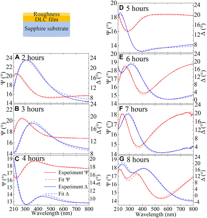
FIGURE 5. Ψ and Δ spectra measured at 70° (A) the 2 h sample, (B) the 3 h sample, (C) the 4 h sample, (D) the 5 h sample, (E) the 6 h sample, (F) the 7 h sample and (G) the 8 h sample. The fit is also included.
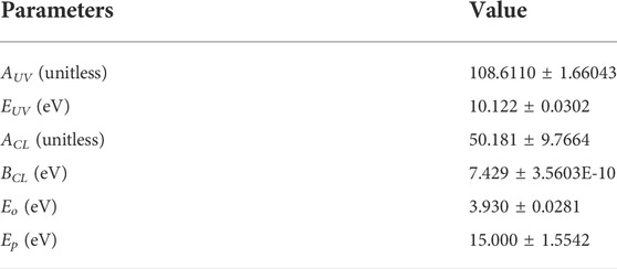
TABLE 1. Fitting parameters of Cody-Lorentz oscillator.
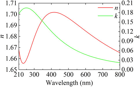
FIGURE 6. Refractive index n and extinction coefficient k spectra of the DLC films.
When the model described above was applied to the DLC films expected to be thinner, with a deposition time of less than 2 h, we found that it could fit also reasonably well with the experimental data but it leaded to vanishing values of the film thickness and increasing values of the roughness overlayer. For very thin DLC films there are many factors that can significantly affect the ellipsometric response, such as surface roughness, the lack of uniformity in the film and the pre-growth instability [31]. Therefore, in an attempt to use a model that is more suitable for these very thin films, but without having to assume different optical constants for the amorphous carbon layer, we represented the films by a single EMA layer, which consisted of a mixture of air and DLC, represented by the same optical constants as in Figure 6. The fit results of this model using only a single overlayer are shown in Figure 7 and Table 2.
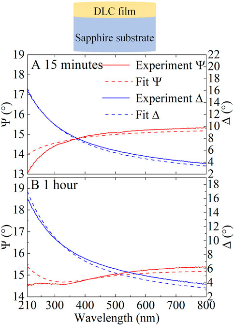
FIGURE 7. Ψ and Δ spectra measured at 70° (A) the 15 min sample and (B) the 1 h sample. The simulated data corresponding with one single EMA model are also included.
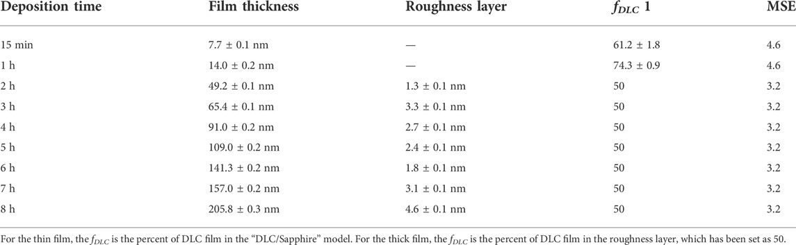
TABLE 2. Fitting results of DLC films for different deposition time.
Table 2 summarizes the results of the ellipsometry analysis. Data corresponding to deposition time of less than 2 h are fitted with the ”DLC film/sapphire” model, while all the other measurements are fitted with the three-layer model. It can be seen that our simple model, based on one single oscillator defined by the parameters given in Table 1, offers good fitting results in all samples.
As a further check, in some samples, we performed ellipsometry measurements at five different points of the surface, which were clearly separated in space (the spot size of the ellipsometer was around 1 mm in diameter). The results obtained at these different points of the surface are in good agreement with those given in Table 2 (that correspond to the center of the sample). For example, for the sample with 6 h deposition, the average and standard deviation values measured after performing measurements at five different points of the surface are 143.7 ± 3.0 nm.
3.3 Transmission electron microscope analysis for verification of SE results
To verify the results of SE, the cross-sectional sample of amorphous carbon film was prepared for TEM observation. Figure 8 shows the cross-sectional TEM image of the amorphous carbon film with deposition time of 15 min, 1 h and 4 h. As Figure 8A shows, when the film was deposited for 15 min, it appears as very uneven or discontinuous. The largest thickness observed was around 7.31 nm and the smallest thickness was 0 nm because an area without deposition was observed. Overall, the “average” thickness approaches the result of ellipsometry fitting as shown in Table 2. The error between ellipsometry and TEM may be caused by the uneven initial growth of the film and the different measurement positions. When the film was deposited for 1 h, it appears to be more continuous and flat as shown in Figure 8B shows two typical thicknesses 9.91 and 13.25 nm (variation up to ∼30%), which are around the result of ellipsometry fitting. After 4 h of deposition, a relatively uniform film can be seen in Figure 8C. The thickness of this area ranges from 90.20 nm to 94.88 nm (variations up to
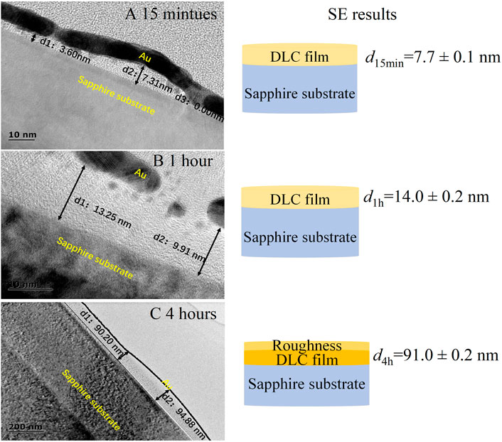
FIGURE 8. Film thickness with different deposition time by TEM cross-sections. Film deposition for 15 min sample (A), for 1 h sample (B), for 4 h sample (C).
Compared to the TEM results, ellipsometry is a non-destructive method to characterize the thickness of the film. The relative error between the TEM and SE results can be defined by
4 Conclusion
In summary, the growth process of thickness and optical properties of amorphous carbon films deposited on the sapphire substrates has been investigated using ellipsometry together with 3D profilometry, Raman spectrometry and TEM. Surface roughness is reported to show some small changes when the film is formed. The characteristic peaks of films by Raman are used to determine whether there is DLC film on the substrate. Spectroscopic ellipsometry is more sensitive to the film thickness, and it can also determine the optical constants (refractive index and the extinction coefficient) of the films. Ellipsometry measurements have been fitted with a suitable optical model, which is a three-layer model for thick film and an EMA model for thinner films (d < 20 nm) respectively. A robust fit of the optical constants of DLC films was achieved with a dispersion function containing only one oscillator. SE thickness results for different deposition time have been checked using TEM cross-sections. Although there is a large relative error comparing with the TEM results for thin films (d < 20 nm) because of the nonuniform deposition in the beginning, SE can still provide an indicator for the trend of thickness growth and accurately characterized the uniform films thickness and optical constants.
Our results suggest that despite the optical properties of amorphous carbon films are closely related not only to the preparation conditions but also to the dynamic growth process of the films, once a stable dynamic growth is achieved the optical constants are maintained over films with large variation in thickness. It is reasonable to speculate that the internal physical or chemical effects in the film-forming process may change the growth conditions of the film. For example, endothermic and exothermic may affect the local growth temperature, thus affecting the changes of sp2 and sp3 contents. Therefore, we believe that a basic understanding of the basic mechanism of optical properties in the growth process of amorphous carbon films is very important for optimizing the application of amorphous carbon films and devices based on amorphous carbon films in the optoelectronic industry. Results from this study will play a role in the future application of combing sapphire substrate and DLC film.
Data availability statement
The original contributions presented in the study are included in the article/Supplementary Material, further inquiries can be directed to the corresponding authors.
Author contributions
All authors discussed the experiment design and contents of the manuscript. Under the supervision of CC, XX oversaw the experiment and analysis. XZ provided the amorphous films. The paper was mainly written by ZL, with assistance from CC and OA for advice and proofreading. SB provided the experimental instruments. XX provided the funding support for the whole work. The experimental results were primarily evaluated and discussed by all authors. All authors have read and agreed to the published version of the manuscript.
Funding
This study was supported by the National Natural Science Foundation of China (Grant No. 51835004).
Conflict of interest
The authors declare that the research was conducted in the absence of any commercial or financial relationships that could be construed as a potential conflict of interest.
Publisher’s note
All claims expressed in this article are solely those of the authors and do not necessarily represent those of their affiliated organizations, or those of the publisher, the editors and the reviewers. Any product that may be evaluated in this article, or claim that may be made by its manufacturer, is not guaranteed or endorsed by the publisher.
References
1. Takabayashi S, Hayashi H, Yang M, Sugimoto R, Ogawa S, Takakuwa Y. Chemical structure and electrical characteristics of diamondlike carbon films. Diam Relat Mater (2018) 81:16–26. doi:10.1016/j.diamond.2017.11.005
2. Xiao H, Zhu J, Han J, Tan M, Jia Z, Jiang C. Stress, mechanical and adhesion properties of multilayer tetrahedral amorphous carbon films. Appl Surf Sci (2008) 255:607–9. doi:10.1016/j.apsusc.2008.06.087
3. Chiu SM, Lee SC, Wang CH, Tai FC, Chu CW, Gan D. Electrical and mechanical properties of dlc coatings modified by plasma immersion ion implantation. J Alloys Compd (2008) 4499:379–83. doi:10.1016/j.jallcom.2006.02.108
4. Wei J, Guo P, Liu L, Li H, Wang A, Wang S, et al. Corrosion resistance of amorphous carbon film in 3.5 wt% nacl solution for marine application. Electrochimica Acta (2020) 346:136282. doi:10.1016/j.electacta.2020.136282
5. Tamuleviĉienė A, Meŝkinis A, Kopustinskas V, Tamuleviĉius S. Multilayer amorphous hydrogenated carbon (a-C:H) and SiOx doped a-C:H films for optical applications. Thin Solid Films (2011) 519:4004–7. doi:10.1016/j.tsf.2011.01.181
6. Reddy KN, Varade A, Krishna A, Joshua J, Sasen D, Chellamalai M, et al. Double side coating of dlc on silicon by rf-pecvd for ar application. Proced Eng (2014) 97:1416–21. doi:10.1016/j.proeng.2014.12.423
7. Oliveira MH, Silva DS, Côrtes ADS, Namani MAB, Marques FC. Diamond like carbon used as antireflective coating on crystalline silicon solar cells. Diam Relat Mater (2009) 18:1028–30. doi:10.1016/j.diamond.2009.01.018
8. Ankit K, Varade A, Reddy KN, Dhan S, Krishna P, Chellamalai P, et al. Synthesis of high hardness ir optical coating using diamond-like carbon by pecvd at room temperature. Diam Relat Mater (2017) 78:39–43. doi:10.1016/j.diamond.2017.07.008
9. Friel I, Geoghegan S, Twitchen D, Scarsbrook GA. Development of high quality single crystal diamond for novel laser applications. In: C Lewis, D Burgess, R Zamboni, F Kajzar, and EM Heckman, editors. Optics and photonics for counterterrorism and crime fighting VI and optical materials in defence systems technology VII. SPIE (2010). p. 340–7.
10. Mesa B, Magonov S. Novel diamond/sapphire probes for scanning probe microscopy applications. In: E Name1, and E Name2, editors. Journal of physics: conference series. IOP Publishing (2007). p. 154.
11. Wei Q, Narayan J. Superhard diamondlike carbon: Preparation, theory, and properties. Int Mater Rev (2013) 45:133–64. doi:10.1179/095066000101528340
12. Ohtake N, Hiratsuka M, Kanda K, Akasaka H, Saitoh H, Hirakuri K, et al. Properties and classification of diamond-like carbon films. Materials (2021) 1:315. doi:10.3390/ma14020315
13. Schwan J, Ulrich S, Batori V, Ehrhardt H, Silva SRP. Raman spectroscopy on amorphous carbon films. J Appl Phys (1996) 80:440–7. doi:10.1063/1.362745
14. Solomon I, Bhatnagar M, Shukla K, Sarma B, Ranjan M, Sarma A. Correlation of structural and optical properties of PVD grown amorphous carbon thin films. Diam Relat Mater (2017) 75:69–77. doi:10.1016/j.diamond.2017.01.015
15. Marcinauskas L, Dovydaitis V, Iljinas A, Andrulevicius M. Structural and optical properties of doped amorphous carbon films deposited by magnetron sputtering. Thin Solid Films (2019) 681:15–22. doi:10.1016/j.tsf.2019.04.055
16. Franta D, Zajíĉková L, Ohlídal I, Janĉa J, Veltruská K. Optical characterization of diamond-like carbon films using multi-sample modification of variable angle spectroscopic ellipsometry. Diam Relat Mater (2002) 11:105–17. doi:10.1016/S0925-9635(01)00528-3
17. Mori T, Fujii N, Xiong YM, Saitoh T. Optical study of ion-deposited diamond-like carbon films using spectroscopic ellipsometry. Thin Solid Films (2013) 7:215–9. doi:10.1016/0040-6090(95)06894-5
18. Hiratsuka M, Nakamori H, Kogo Y, Sakurai M, Ohtake N, Saitoh H. Correlation between optical properties and hardness of diamond-like carbon films. J Solid Mech Mater Eng (2013) 7:187–98. doi:10.1299/jmmp.7.187
19. Zhou XL, Suzuki T, Nakajima H, Komatsu K, Kanda K, Lto H, et al. Structural analysis of amorphous carbon films by spectroscopic ellipsometry, rbs/erda, and nexafs. Appl Phys Lett (2017) 110:201902–5. doi:10.1063/1.4983643
20. Zhou XL, Arakawa S, Tunmee S, Komatsu K, Kanda K, Ito H, et al. Structural analysis of amorphous carbon films by bema theory based on spectroscopic ellipsometry measurement. Diam Relat Mater (2017) 79:46–59. doi:10.1016/j.diamond.2017.08.002
21. Peckus D, Meškinis Š, Vasiliauskas A, Rajackaitė E, Andrulevičius M, Kopustinskas V, et al. Structure and optical properties of diamond like carbon films containing aluminium and alumina. Appl Surf Sci (2020) 529:147040. doi:10.1016/j.apsusc.2020.147040
22. Yang Q, He S, Huang R, Yu M, Chen C, Zheng S, et al. Research on the fabrication and anti-reflection performance of diamond-like carbon films. Diamond Relat Mater (2021) 111:108184. doi:10.1016/j.diamond.2020.108184
23. Nichols S, Arteaga O, Martin A, Kahr B. Measurement of transmission and reflection from a thick anisotropic crystal modeled by a sum of incoherent partial waves. J Opt Soc Am A (2015) 32:2049–57. doi:10.1364/JOSAA.32.002049
24. Arteaga O, Freudenthal J, Wang BL, Kahr B. Mueller matrix polarimetry with four photoelastic modulators: theory and calibration. Appl Opt (2012) 51:6805–17. doi:10.1364/AO.51.006805
25. Yu NS, Guo LW, Peng MZ, Zhu XL, Wang J, Jia HQ, et al. Micro-raman spectroscopy characterization of gan grown on maskless periodically grooved sapphire fabricated by wet chemical etching. Chin J Liq Cryst Disp (2010) 25:17–20. doi:10.3969/j.issn.1007-2780.2010.01.004
26. Raml C, He XN, Han M, Dennis RA, Lu YF. Raman spectroscopy based on a single-crystal sapphire fiber. Opt Lett (2011) 36:1287–9. doi:10.1364/OL.36.001287
27. Cloude SR. Conditions for the physical realisability of matrix operators in polarimetry. In: RA Chipman, editor. Polarization considerations for optical systems II. International Society for Optics and Photonics (1990). p. 177–87.
28. Roychowdhury T, Shah D, Hilfiker JN, Linford MR. Polymethyl methacrylate: Optical properties from 191 to 1688 nm (0.735–6.491 ev) by spectroscopic ellipsometry. Surf Sci Spectra (2020) 27:016002. doi:10.1116/1.5095422
29. Ferlauto A, Ferreira G, Pearce JM, Wronski C, Collins R, Deng X, et al. Analytical model for the optical functions of amorphous semiconductors from the near-infrared to ultraviolet: Applications in thin film photovoltaics. J Appl Phys (2002) 92:2424–36. doi:10.1063/1.1497462
30. Takabayashi S, Hayashi H, Yang M, Sugimoto R, Ogawa S, Takakuwa Y. Model-free determination of the birefringence and dichroism in c-cut crystals from transmission ellipsometry measurements. Appl Opt (2020) 59:2192–200. doi:10.1364/AO.386583
Keywords: amorphous carbon film, film thickness, optical constants, film uniformity, spectroscopic ellipsometry
Citation: Li Z, Cui C, Zhou X, Bian S, Arteaga O and Xu X (2022) Characterization of amorphous carbon films from 5 nm to 200 nm on single-side polished a-plane sapphire substrates by spectroscopic ellipsometry. Front. Phys. 10:968101. doi: 10.3389/fphy.2022.968101
Received: 13 June 2022; Accepted: 15 September 2022;
Published: 03 October 2022.
Edited by:
Steen Grüner Hanson, Technical University of Denmark, DenmarkReviewed by:
Mathias M. Schubert, University of Nebraska-Lincoln, United StatesMati Horprathum, National Electronics and Computer Technology Center, Thailand
Copyright © 2022 Li, Cui, Zhou, Bian, Arteaga and Xu. This is an open-access article distributed under the terms of the Creative Commons Attribution License (CC BY). The use, distribution or reproduction in other forums is permitted, provided the original author(s) and the copyright owner(s) are credited and that the original publication in this journal is cited, in accordance with accepted academic practice. No use, distribution or reproduction is permitted which does not comply with these terms.
*Correspondence: Changcai Cui, Y3VpY2hjQGhxdS5lZHUuY24=; Oriol Arteaga, b2FydGVhZ2FAdWIuZWR1