
94% of researchers rate our articles as excellent or good
Learn more about the work of our research integrity team to safeguard the quality of each article we publish.
Find out more
ORIGINAL RESEARCH article
Front. Phys., 03 October 2022
Sec. Radiation Detectors and Imaging
Volume 10 - 2022 | https://doi.org/10.3389/fphy.2022.957991
 Anna Paola Caricato1,2*
 Sandra Moretto3
 Maria Rachele Guascito4
 Gianluca Quarta1,2,5
 Marco Mazzeo1
 Matteo Favaro6,7
 Muhammad Rizwan Aziz1
 Chiara Provenzano2,8
 Marcella Marra1,2
 Maura Cesaria1
 Matteo Polo3
 Jessica Delgado3
 Felix Pino3
 Maurizio Martino1,2
 Lucio Calcagnile1,2,5
 Alberto Quaranta6,7
Although the field of solar cells is the most popular application of perovskite materials, their use in radiation detection applications is emerging. The success of perovskites as radiation detectors rests partly on the same material properties that have led to successful optoelectronics applications, meaning that other specific properties, like large stopping power, high mobility lifetime product, fast response, and large bulk resistance, play a role. In this respect, inorganic perovskites are attracting a lot of attention as scintillator materials with performances sensitive to material shape (single crystals, nanocrystals, and thin films) and growth methods. In this study, we report on the morphological, structural, and optical response of thin CsPbBr3-based perovskite films, deposited by Pulsed Laser Deposition (PLD) and post-growth annealed at 350°C in air, following excitation by different particle sources. The annealing treatment resulted in a prompt structural refinement, grain growth, and oxygen bonding to the Pb phase together with an enrichment of the surface in chemo-adsorbed oxygen probably due to Cs–O interactions, as evidenced by X-ray photoelectron spectroscopy. The film behavior under 2 MeV H+ ion beam irradiation at different fluences was analyzed together with its scintillation properties following an interaction with α particles from an Am-241 radioactive source demonstrating a very fast response for an inorganic material (∼5ns) and a photoelectron yield of about ∼47% with respect to a commercial CsI:Tl scintillator.
Halide perovskites with a general formula of AMX3 (where “A” and “M” are cations with A+ = Cs, CH3NH3, and HC (NH2)2 and M2+ = Ge, Sn, and Pb, while “X” is an anion with X− = Cl, Br, and I) have attracted a lot of interest because of their appealing properties like long carrier diffusion lengths, defect tolerance, high photoluminescence (PL) quantum yields, and band gaps tunable by doping and changes in phase/composition making them interesting for many applications [1,2,3,4,5,6,7]. In particular, the outstanding high photoluminescence quantum yield of these materials is a key feature enabling bright light-emitting devices and lasers [8,9,10], whereas the high current conversion efficiency underpins their application as photodetectors and solar cells [8,11,12,13].
Recently, perovskite materials are also emerging as a promising new generation of ionization detection materials because, in addition to the aforementioned good properties, they exhibit large mobility of charge carriers, low cost, and good γ-ray hardness and strong stopping power [14,15,16]. For radiation detection applications, inorganic perovskites have large effective X-ray stopping power due to the high atomic number of the constituent elements (like Pb, Br, and I atoms). For example, CsPbBr3 is a high-Z compound with an effective atomic number of Zeff = 65.9. Single-crystal CsPbBr3 detectors for hard X- and γ-rays have demonstrated excellent energy resolution comparable with the capability of commercially available detectors [17].
As radiation detectors, perovskite-based scintillators could offer, in principle, unique advantages as compared to conventional scintillation materials, in terms of performance, low cost, flexibility, high quantum yield, strong absorption, and fast response (less than 20 ns) [18,19,20]. Very fast response scintillators are strategic, for example, for advanced radiometry applications like medical imaging in positron emission tomography and for high-energy physics experiments in high-luminosity colliders, where high event rates require a fast response.
Moreover, perovskite-based scintillators offer the possibility to tune photon emission across the visible spectrum by changes in the anionic component of the material and enhanced coupling with photon detectors [19].
The first demonstration of the role of fast radiative decay of excitons in scintillation from halide perovskites dates back to 1993 when very fast and intense X-ray luminescence of excitons in CsPbX3 was first observed [21], whereas, at first, the light yield of single-crystal CsPbBr3 scintillators at room temperature was found to be very low under γ excitation, that is, <330 Ph/MeV [22], research efforts in the fabrication of CsPbX3 single crystals and nanocrystals contributed to achieving interesting and promising results over the years in terms of low detection limit [13 nG y/s−1 was recorded for a thin-film scintillator device, which is much lower than the dose typically used for X-ray diagnostics (5.5 μGy s−1), very fast response to X-rays (4.6 ns) [19]] and high scintillation light yield both at room temperature and cryogenic temperatures [23,24].
Highly sensitive scintillation screens for X-ray imaging using CsPbX3 nanocrystals were reported too [19,25,26].
Most of these encouraging results refer to X-ray-, γ-ray-, or α-particle-induced scintillation in single crystals whose growth is time-consuming and their application in flexible architectures is not allowed. However, very few articles report on scintillation properties of perovskite films [27] for which two different approaches are generally used for their growth based on solution-based methods [28,29,30,31] and dry vacuum with [32,33,34,35,36].
Although inexpensive, solution-based methods to grow perovskite nanocrystals and films, with X- and γ-induced scintillation properties may be problematic due to many practical drawbacks (toxic chemicals, solubility in different solvents of the precursor salts, and occurrence of multiple Cs-Pb-Br compounds) and processing steps of manufacturing [37]. Among dry vacuum-assisted methods, vacuum thermal evaporation enables the growth of large-area single and multilayered films with fine control on thickness, uniformity, and composition. However, the growth of multication–multihalide materials by thermal evaporation requires two evaporation sources and fine control of complex procedures because of the different evaporation rates of the involved source materials [37].
Pulsed laser deposition (PLD) is a leading technique in depositing multi-component materials with complex stoichiometry due to allowing congruent transfer of stoichiometry [38,39,40,41]. However, the peculiar composition of perovskite materials containing elements with very different mass ratios (in the case of CsPbBr3, Pb is much heavier than Cs and Br) is responsible of preferential scattering of light elements in the plasma plume, hence making difficult to obtain the exact stoichiometry. Recently, a flexible interplay between the deposition parameters was demonstrated to be effective to enable a fine control of composition and uniformity properties of the PLD deposit [37,42].
In this study, we report on the scintillation response to α-particles, emitted by an Am-241 source, of thin CsPbBr3-based perovskite films deposited by PLD under properly controlled experimental conditions. In this respect, optimal growth conditions and post-growth annealing are discussed based on a rich series of characterizations (structural, compositional, spectral, and photoluminescence analyses). Such investigation is particularly important because good quality films are a fundamental prerequisite for efficient scintillation yield. Indeed, as a result of carefully calibrated preparation protocols, high scintillation yield and fast response to alpha particles are demonstrated and discussed.
Halide perovskite CsPbBr3 films were deposited by nanosecond-PLD using the experimental setup depicted in Figure 1. As a result of the interaction between a pulsed excimer laser beam and the target material, a forwardly peaked plasma plume generates and it drives the transfer of the ablated material onto the substrate, where the film forms. Operatively, a focused KrF pulsed laser beam (Lambda Physik), operating at the wavelength λ = 248 nm and pulse width τp = 20 ns, was directed at 45° on the surface of a mechano-chemically synthesized CsPbBr3 solid target placed within a stainless-steel deposition chamber. The CsPbBr3 target was prepared by mixing, for 15–20 min at room temperature, a 1:1 M ratio of CsBr and PbBr2 precursor powders purchased from chemPUR (99.9% purity). The pressed pellet was transferred to an oven for thermal treatment (2 h at 400°C followed by 2 h at 500°C). The resulting target was mounted on a rotating and XY-motorized holder. During the film growth, the substrate was rotated at a rotation frequency of 1.2 Hz to avoid drilling and formation of craters on the irradiated area.
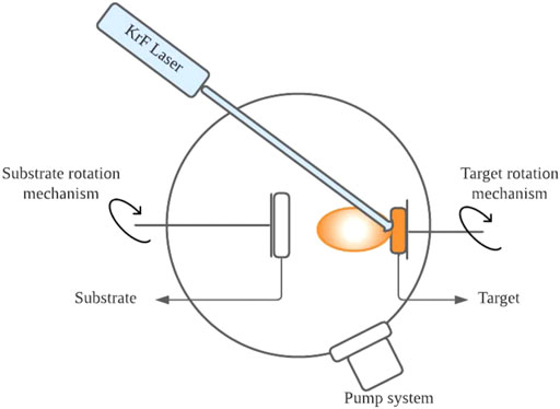
FIGURE 1. Schematic depiction of a setup for pulsed laser deposition (PLD) experiments including a stainless-steel high-vacuum chamber, a rotating target holder, a substrate holder, and a pumping system. Operatively, a pulsed excimer laser beam generates a forwardly peaked plasma plume while interacting with a target material and the transfer of the ablated material onto the substrate forms the deposit.
Before starting PLD, the vacuum chamber was evacuated to a background pressure of 10−5 Pa using a combined (rotative plus turbo-molecular) pumping system. For the film deposition, the laser fluence and frequency were fixed to 1 J/cm2 and 5 Hz, respectively. The ablated species were collected on silica substrates (carefully cleaned in an acetone and ethanol ultrasonic bath for 10 min) kept at room temperature during the depositions, placed at the target–substrate distance of dT-S = 4 cm and with substrate-axis shifted by ∼ 4 mm with respect to the plume axis.
For the deposition conditions detailed previously, a film deposition rate of 0.4 nm/s was estimated by measuring the film thickness vs. the number of laser pulses.
While 130-nm-thick perovskite-based films were grown by PLD for calibrating the deposition rate as a function of the laser fluence and for characterization purposes, 1-µm-thick films were used for the scintillation tests.
The as-grown CsPbBr3 perovskite films were post-growth annealed in air at 350°C for 45 min (ramp = 5°/min) according to a thermal heating protocol setup to induce morphological evolution toward stable structural and emission properties without changes in the film stoichiometry.
Film surface topography and root-mean square roughness (RMS, Rq), estimated over 20 μm × 20 µm wide area, were investigated by atomic force microscopy (AFM, Park XE-70 Instruments) operating in a non-contact mode, at room temperature and in an air environment. It was used a silicon cantilever with a tip radius of about 10 nm, a spring constant of K = 0.1–100 N/m and a resonance frequency of about 300 kHz. The Rq values reported are an average calculated over five measurements acquired in different representative areas of the films. The uncertainty refers to the standard deviation of the series of measured values.
The microstructure of the perovskite films deposited by PLD on silica substrates was investigated by the X-ray diffraction (XRD) technique by means of a Rigaku MiniFlex diffractometer, operating in a step-scan mode and employing a Cu-Kα X-ray source of wavelength 1.54056 Å, working with 40 kV voltage and 20 mA operating current. The XRD diffractograms were acquired over the angular range 2θ from 10 to 40 deg, with a 0.020 deg step-size.
In order to determine the film composition, Rutherford backscattering (RBS) analyses were performed using a 2 MeV 4He2+ ion beam accelerated by a 3 MV Tandetron accelerator (High Voltage Engineering Europa BV Mod. 4130HC).
The backscattered particles, at an angle of 170°, were detected by using a PIPS (passivated implanted planar silicon) detector with a solid angle of 3 msr [43]. The number of ions reaching the samples was calculated from the total deposited charge obtained by integrating the beam current reaching the samples mounted on the electrically isolated vacuum chamber. Spectra were acquired and pre-processed by using GENIE software from Canberra. The experimental data were fitted in order to obtain film composition and density by using the SIMNRA package [44].
The elemental atomic composition and chemical surface speciation were determined using an Axis Ultra DLD (Kratos Analytical) spectrometer for X-ray photoelectron spectroscopy (XPS) analysis, equipped with an Al Kα (1486.6 eV) monochromatic source, operating at 10 kV and 15 mA. The pressure in the analysis chamber was 1.2 × 10⁻⁹ torr. Spectra acquisition was performed in a fixed analyzer transmission (FAT) mode, at a pass energy of 160 eV for survey scan (step size 1 eV) and 20 eV for high-resolution (HR) spectra acquisition (step size 0.1 eV). The analyzed area was 700 μm × 300 µm. All the experimental binding energy values were corrected by setting the binding energy of the C1s hydrocarbon photo-electron line at 285.0 eV used as an internal standard [45,46]. Data analysis was performed using the fitting program CasaXPS. Peak assignments were carried out by comparing the binding energy to the literature data and using the NIST standard reference database [47]. Peak areas, as obtained from peak fitting, were converted to the atomic percent composition (At%) using the suitable sensitivity factors (SFs) [48]. All obtained atomic percentage compositions were representative of the mean values obtained on minimum three different spots of the same sample.
Optical transmission measurements in the UV-Vis spectral region were performed using a double-beam grating UV spectrophotometer Perkin Elmer model Lambda 900, covering the spectral range from 250 to 800 nm and with a wavelength resolution of 3 nm. The absorption coefficient was calculated by the method described elsewhere [49], and the energy band gap was estimated by means of the Tauc’s plot approach.
The optical response of the perovskite films under consideration in this study to ion bombardment was investigated by ion beam-induced luminescence (IBIL) at the AN2000 accelerator of INFN Laboratori Nazionali di Legnaro using a 2 MeV H+ ion beam with a fluence rate of 9·1011 H+/cm2 s. The emitted light was collected using a 600 μm MM silica fiber and analyzed using an Ocean Optics QE65000 spectrometer (200–1100 nm). The integration time was set to 1 s.
To study the scintillation properties of the CsPbBr3-based perovskite sample, in particular the decay time of the scintillation signals and the light output, an Am-241 calibration alpha source was employed (Eα ∼5.5 MeV, activity ∼30 kBq). The samples were optically coupled to a 1” diameter photomultiplier tube, Hamamatsu H6524, and the alpha source was in the opposite face of the sample. There was a 4 mm of air gap between the source and the sample. The experimental setup is presented in Supplementary Figure S1. The PMT signals were acquired and pre-processed using a CAEN Desktop digitizer DT5725 (14-bit ADC resolution and 250 MHz of the sampling rate). The firmware installed on the digitizer, namely, digital pulse processing for charge integration and pulse shape discrimination (DPP-PSD), allows to pre-process the data, determining the event timestamps and integrating the signals. The pulse height spectrum can be generated using the total integral of the signals. To determine the decay time of the scintillation signals, a set of waveforms was digitized using a Teledyne LeCroy oscilloscope HDO4104 model, having 12-bit ADC resolution, 1 GHz bandwidth and sampling up to 2.5 GS/s.
The PMT was operated at −1600 V. The bias voltage was applied using a CAEN V6533 VME HV Power Supply Module. A CAEN V2718 VME-PCI Optical Link Bridge was used to control the HV power supply unit. A CAEN A3818 PCI Express CONET2 Controller installed on a desktop PC was used to configure and control the digitizer and the HV power supply unit (by means of optical fiber connections using the CAEN CONET2 protocol).
All parameters of the electronics, and also of the data acquisition, were managed using ABCD (Acquisition and Broadcast of Collected Data) software [50,51], as an open-source project1.
In order to perform a quantitative comparison of the light output exhibited by the CsPbBr3-based perovskite sample, a similar experiment was carried out using a thallium-doped cesium iodide (CsI:Tl) standard inorganic scintillator (12 mm × 19 mm × 20 mm).
Topography measurements of the as-grown film and post-growth thermally treated at 350°C perovskite film under consideration in this study are reported in Figure 2 that shows a compact pinhole-free background and a foreground consisting of columnar grains, with a size ranging from tens of nanometers to a few hundreds of nanometers. The RMS roughness value of about 60 nm was estimated over a 20 μm × 20 μm area for the annealed film. Columnar-like grains were already observed in the case of past experiments we performed at room temperature [37]. Evidence of coalescence mechanisms can be observed on comparing Figures 2A,B: thermal annealing treatment results in enhanced evolution toward columnar growth of grains and increase in their size. On accounting for the peculiar PLD mechanisms (high-saturation and hyper-thermal deposition flux), high-density distribution of small grains can be observed in the case of the as-grown film (Figure 2A). The finely grained background exhibited by the annealed film can be confidently ascribed to the growth of the high-density nucleation seeds formed due to the supersaturated deposition flux. On progressing the deposition, further growth of grains and agglomeration mechanisms can explain the formation of a two-fold grain distribution and the morphological evolution of large islands favored by hyperthermal surface kinetics too.
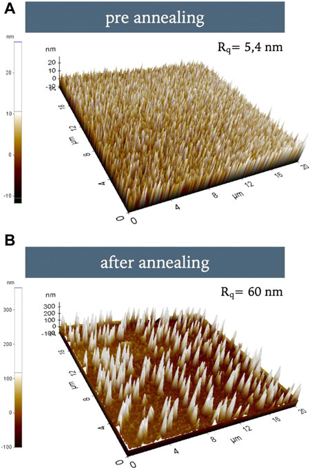
FIGURE 2. AFM image of a PLD-deposited perovskite film (A) before and (B) after thermal treatment at 350°C. Columnar morphological evolution and increase in size of grains can be observed.
Analysis on the crystalline nature of the film under study investigated by the XRD analysis is reported in Figure 3: spectra indicate a polycrystalline nature and the coexistence of multiple phases of the Cs-Pb-Br ternary compound. This issue is not surprising on accounting for the fact that the 1:1 molar ratio of PbBr2: CsBr was set for preparing the targets that makes highly unlikely the occurrence of PbBr2 in excess able to drive the reaction 3PbBr2 + Cs4PbBr6 → 4 CsPbBr3 and the formation of the Pb-rich CsPb2Br5 phase.
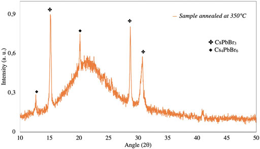
FIGURE 3. XRD spectra of PLD-deposited perovskite-based films thermally annealed at 350°C following growth at room temperature. The peaks associated with the observed Cs-Pb-Br ternary compounds are indicated, that is., CsPbBr3 and Cs4PbBr3.
In addition to a main broad band that is ascribed to the amorphous phase of the silica substrate, refined peaks occur. In particular, the peaks at 2θ = 15.16, 28.68, and 30.68 deg correspond to the characteristic peaks of the CsPbBr3 phase associated with the (100), (110), and (200) crystal lattice planes (pdf card #18-0364) of the cubic phase, respectively. The slight peak broadening/splitting at nearly 15.16 and 30.68 deg may indicate the occurrence of the residual orthorhombic phase, meaning the two-phase CsPbBr3 coexistence. The peaks at 2θ = 12.66 and 2θ = 20.14 deg are associated with the Cs-rich Cs4PbBr6 phase (pdf card #73-2478).
Moreover, post-growth annealing also favors the preferred growth of crystals with (110) orientation rather than the (200) one. In Table 1, the grain sizes corresponding to the different lattice planes for the annealed films are reported as determined using the Scherrer formula [52].
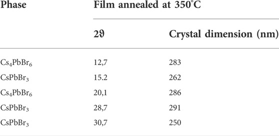
TABLE 1. Dimensions of crystalline phases and grains of PLD as-deposited and annealed (350°C) perovskite-based films
The RBS analysis was performed on the films deposited on silica substrates to determine the film composition. From the spectra simulation based on the SIMNRA package, the film composition resulted to be Cs0.26Pb0.22Br0.53 with an uncertainty of 2%. For the sake of completeness, the RBS spectrum under consideration is reported in Supplementary Figure S2. The quoted composition indicates the presence of a slight excess in Cs and deficiency in Br, in agreement with the discussion reported elsewhere [37] and the observed occurrence of the Cs-rich phase Cs4PbBr6 in our film. Furthermore, since the RBS technique does not enable to determine the eventual presence of oxygen physi-sorbed/adsorbed on the film surface due to the dominant contribution from the SiO2 substrate, the XPS spectra were acquired (Figures 4, 5). This aspect has to be considered because it is well known that perovskite halide nanocrystals suffer from instability issues, and, in particular, photoluminescence of CsPbBr3 may be affected by exposure to air and moisture [53].
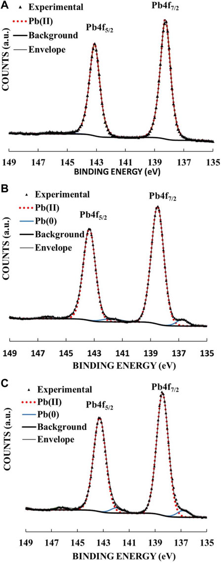
FIGURE 4. Typical high-resolution XPS spectra of Pb4f photoelectron lines with the relevant curve fitting for the CsPbBr3 target (A) and PLD-deposited perovskite-based film before (B) and after (C) being submitted to a post-deposition annealing treatment at 350°C. Refer to the text for the chemical assignment to the components of the individual pair of peaks as indicated in the legends.
Together with the XPS spectrum of the CsPbBr3 film of interest in this study, the XPS analysis of CsPbBr3 mechanochemically synthesized, the target and the CsPbBr3 as deposited film was acquired too (Supplementary Figure S3). As expected, the most intense signals are related to Cs [i.e., Cs3d, Cs3p, and Cs (MNN)], Pb (i.e., Pb4f and Pb4d), and Br (i.e., Br3d and Br3p) photo-peaks. However, C1s and O1s peak signals related to carbonaceous contamination and/or physi-chemisorbed oxygen can be also observed. Based on the high-resolution region peak fitting, the binding energies of the most intense Cs3d5/2, Pb4f7/2, and Br3d5/2 peaks are (724.5 ± 0.1) eV, (138.4 ± 0.1) eV, and (68.2 ± 0.2) eV, respectively, for all samples. These values are in line with the previous XPS data reported for CsPbBr3-based perovskite [54].
In detail, the shape and the binding energy of Cs3d and Br3d peak signals are the same for all typology of analyzed samples being typically characterized by a well-resolved pair of peaks for both signals: Cs3d (pair of peaks Cs3d5/2-Cs3d3/2) and Br3d (pair of peaks Br3d5/2-Br3d3/2), respectively (Supplementary Figure S4). Differently, the Pb4f photoelectron line of the as-deposited and the post-deposition annealed film (Figures 4B,C), near the intense characteristic pair of peaks at (138.3 ± 0.1) eV (Pb4f7/2) and (143.3 ± 0.2) eV (Pb4f5/2) related to the expected Pb (II), shows a pair of peaks at (136.7 ± 0.2) eV (Pb 4f7/2) and (141.9 ± 0.2) eV (Pb 4f5/2) attributed to a new Pb (0) phase [55]. Typically, the Pb (0) component represents almost 7% of the Pb (II) content in both films. No signal related to Pb (0) is present on the CsPbBr3 target (Figure 4A), where the Pb4f photoelectron peak is dominated only from the signal associated with the Pb (II) pair of peaks.
The analysis of the C1s and O1s high-resolution regions for as-deposited CsPbBr3 film shows the presence of adventitious carbon with a dominant carbonaceous (C-C) component not associated to carbonaceous and/or adsorbed oxygen (data not shown). Otherwise, adventitious carbon and oxygen were detected after 350° annealing. Figure 5 shows that a quantitative oxygen content unrelated to the contamination carbon [i.e., C=O and C-OH at (531.2 ± 0.2) eV and (533.1 ± 0.2) eV, respectively] is now present at (529.3 ± 0.2) eV and can be tentatively attributed to oxygen adsorbed on lead (Pb-Oads), formed with the Pb phase. In addition, the ratio between the carbonaceous oxygen (C-O and C=O) obtained from the carbon fitting [peaks at (286.5 ± 0.1) eV and (288.4 ± 0.1) eV] and the oxygen obtained from the oxygen components [peaks at (531.2 ± 0.2) eV and (533.1 ± 0.2) eV] is almost 0.4, hence indicating an enrichment of the surface in the chemo-adsorbed oxygen content probably due to Cs–O interactions.
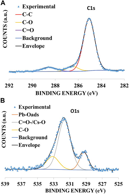
FIGURE 5. Typical high-resolution XPS spectra of C 1 s (A) and O 1 s (B) photoelectron lines with the relevant curve fitting for the PLD-deposited perovskite-based film submitted to a post-deposition annealing treatment at 350°C. Refer to the text for the chemical assignment to the individual peak pair signal components as indicated in the legends.
The oxygen–cesium interaction is confirmed from the Cs-modified Auger parameter [α’ = KE (CsMNN) + BE (Cs3d5/2)] [56], that was (1293.1 ± 0.1) eV for the as-deposited film, as expected for cesium halide (i.e., α’ = 1293.0 eV for CsCl) and increased to (1295.5 ± 0.2) eV after film annealing. The significant α’ increment suggests the formation of a Cs–O interaction causing a strong extra-atomic relaxation in comparison with the oxygen-free surface of the as-deposited film [56]. From the XPS compositional analysis, the surface composition of the annealed film resulted to be Cs0.54Pb0.22Br0.56O0.16. These data highlight some differences in the chemical composition of the film between the bulk (Cs0.26Pb0.22Br0.53) and the surface that results enriched in Cs with respect to the Pb content, although the ratio between Pb and Br is constant. The presence of oxygen on the film surface was also highlighted.
On turning to the optical response of the PLD-deposited CsPbBr3 film under study, the UV-Vis transmittance spectrum in Figure 6A shows two main dips at 310 and 515 nm. The signal between 305 and 330 nm is generally ascribed to the Cs4PbBr6 band gap absorption [57]. The peak at around 520 nm can be attributed to the exciton close to the optical band gap of the CsPbBr3 compound [58,59]. As a result of the performed post-growth annealing treatment, an increase in film transmission was observed, consistently with the observed structural refinement driven by thermal-annealing. The optical band gap was calculated by applying the Tauc’s plot method to the absorption coefficient which was calculated by the procedure reported elsewhere [37]. As a result, the energy band gap was evaluated to be 2.33 eV (Figure 6B). Although this value is slightly smaller than the band gap of bulk CsPbBr3, it is in accordance with other evaluations reported in the literature [60].
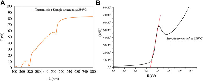
FIGURE 6. (A) UV-Vis transmittance curve of the PLD-deposited perovskite-based film after a post-deposition thermal treatment at 350°C in an oven; (B) evaluation of the band gap energy of the post-growth thermally treated film as extracted from the Tauc’s plot method.
Knowledge of the optical properties is particularly important in this study because a fundamental prerequisite for scintillation is that the film exhibits radioluminescence. As already pointed out, preliminary experiments (not reported here because out of the focus of this study) demonstrated the importance of the post-growth annealing treatment to induce a prompt photoluminescence as a result of refined crystallinity and increased grain size combined with removal of surface states/trapping states and passivation by water vapor. Indeed, the annealed sample demonstrated a bright green emission at 532 nm and a Stokes shift of 17 nm under excitation at 405 nm which is attributed to the exciton recombination due to Br-vacancies [59].
In Figure 7A are shown the IBIL spectra of the perovskite film at the beginning and at the end of the irradiation, while in Figure 7B the peak intensity is shown as a function of the irradiation fluence.
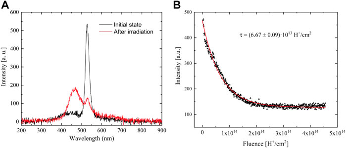
FIGURE 7. (A) IBIL spectra under proton beam at the beginning and at the end of the irradiation run and (B) peak emission (λpeak = 530 nm) intensity decay as a function of the fluence together with the single-exponential fitting function and the decay constant. The broad peak at about 450 nm is a characteristic feature of SiO2 point defects.
The spectral response shows a sharp peak at 530 nm, which decreases down to a stable value after a total fluence of about 1.5 × 10¹⁴ H+/cm2. The broad peak at about 450 nm, whose intensity increases with the irradiation fluence, is a characteristic feature of SiO2 point defects.
The decreasing trend of the perovskite peak can be fitted with a single exponential function [61] with a decay constant of (6.67 ± 0.09) × 1013 H+/cm2.
To date, the effects of proton irradiation on this kind of perovskites was studied only by Zhao et al. [62], where the authors used low-energy ions (50 keV) in order to maximize the vacancy formation in the matrix. Moreover, the damage was correlated to the photovoltaic responsivity of the film. Protons of 2 MeV, going through the whole film thickness, release electronic energy, with a much lower vacancy production, as evidenced by the SRIM analysis. So, the intensity decrease can be attributed mainly to the irradiation-induced desorption of oxygen, whose presence in the network contributes to the enhancement of the excitonic peak. After fluences higher than 1014 H+/cm2, the peak intensity reaches a saturation value, probably due to the attainment of an equilibrium regime of defects and oxygen centers. Further experiments are in progress to support our conclusions that, however, are in line with the findings of the experiments reported.
It is worth noting that, even after quite high fluence values, a residual luminescence is still present, evidencing that the film could keep a detectable scintillation yield. Further analyses on the evolution mechanisms under irradiation and on the correlation with the oxygen retained by the matrix will be carried on in the future.
In order to get a decay time associated with an alpha-induced scintillation event, a set of waveforms was acquired using the Teledyne LeCroy oscilloscope. Then, an average waveform was computed, and a single exponential decay function was fitted to the decreasing part of the waveform (Figure 8). A multiple exponential decay function was tested but better results were obtained using only one exponential function. As a result, a time constant τ = (5.5 ± 1.9) ns was obtained. It is important to remark that in nuclear and particle physics the fastest scintillators are usually organics, which exhibit decay constants of a few nanoseconds. In addition, the usual inorganic scintillators, employed in spectroscopy measurements, are much slower (with decay constants of a few tens or hundreds of nanoseconds), more difficult to handle (most of them are hygroscopic like LaBr3: Ce and CeBr3), and have intrinsic radioactivity (like LYSO and LSO) making their analysis more complex.
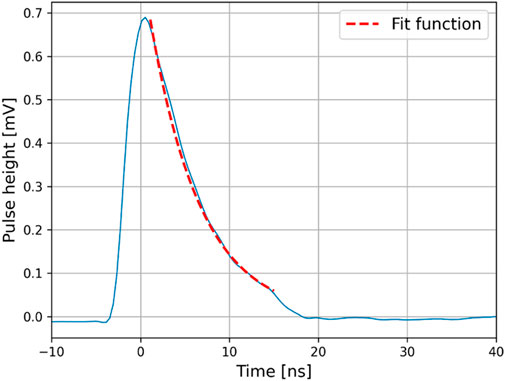
FIGURE 8. Average alpha-induced scintillation waveform of the CsPbBr3-based perovskite sample. A single-exponential decay fit is also shown.
In Figure 9, the pulse height spectrum corresponding to the response of the CsPbBr3-based perovskite sample (1 μm thick.) is reported, when it is irradiated with ∼5 MeV energy alpha particles. The integration gate of the signals was set in 120 ns, starting 20 ns before its leading edge, that is, enough to completely integrate the signal. It is worth to mention that the total integral of the signal is proportional to the total light yield in this event. The Am-241 source emits alpha particles of ∼5.5 MeV in 4 mm of air, and this energy is reduced to ∼5 MeV. Then, in 1 μm of CsPbBr3-based perovskite, these alpha particles deposit an energy between 0.15 and 0.30 MeV (depending on the incident angle). Therefore, the spectrum reported in Figure 9 represents the response of the CsPbBr3-based perovskite sample when this amount of energy is deposited by alpha particles.
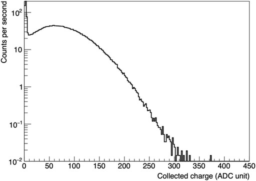
FIGURE 9. Pulse height spectrum corresponding to the response of the CsPbBr3-based perovskite sample (1 micron thick) when it is irradiated with alpha particles of ∼5 MeV
Now, in order to quantify the light yield by the CsPbBr3-based perovskite sample under this condition, we compared its response with the one shown by a standard inorganic scintillator (CsI:Tl). As we do not have a CsI:Tl thin film, we prepared an experimental setup in order to get a calibration curve of the energy deposited by the alpha particle in the scintillator (in MeV) as a function of the light yield (in ADC units). The CsI:Tl has a dimension of 12 mm × 19 mm × 20 mm. It was wrapped with a Teflon tape to reflect and collect most of the light produced. One of the largest faces was covered with 1 μm of aluminized mylar, and the other was coupled optically to the same H6524 PMT, and it was operated at the same bias supply. The loss of energy of the alpha particles in the aluminized mylar window has been neglected. The nuclear electronic chain used to acquire and analyze the data was unaltered (with respect to the one used with the perovskite sample). Since the decay time of the CsI:Tl signals is different to the one observed for the perovskite-based scintillator, the integration gate was set at 6 µs, starting 100 ns before the leading edge. The energy of the incident alpha particle was reduced one step at the time using Kapton [poly (4,4′-oxydiphenylene-pyromellitimide)] absorbers (8, 13, 16, 21, 24, and 26 μm thick), which were attached to the aluminized mylar window of the CsI:Tl crystal. The energy deposition in all involved materials (air gap, Kapton, mylar, and scintillator) was taken into account. The calculations of the energy deposited in the CsI:Tl crystal in each configuration were performed using LISE++ software [63]. Being standard materials, the specifications of the materials used for the calculations were found on the database of software. Despite the large spread of energy deposited in CsI:Tl, as in the case of the perovskite-based scintillator, the analysis was based on the end point of the pulse height spectrum that corresponds to the maximum energy deposited in the crystal. In Figure 10, the calibration curve obtained with the measurements performed with the CsI:Tl crystal is reported. The error bars of the energy deposited are mainly due to the uncertainties of the thickness of the absorbers (2 μm). Furthermore, over the CsI:Tl calibration curve, we report the point (red mark) that corresponds to the light yield exhibited by the CsPbBr3-based perovskite sample with an alpha particle depositing 0.30 MeV.
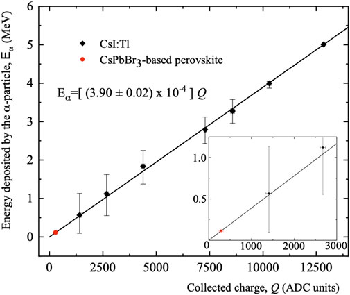
FIGURE 10. Calibration curve of the maximum energy deposited by the alpha particle in the CsI:Tl crystal as a function of the collected charge (that is, proportional to the light yield). The read point corresponds to the collected charge observed when an alpha particle deposits 0.30 MeV in the CsPbBr3-based perovskite sample. The inset shows a zoom area to observe better the position of the red point.
It can be concluded that the 0.30 MeV alpha particles in the perovskite sample produces the same photoelectric current of an alpha particle of about ∼0.14 MeV in CsI:Tl. In other words, the total photoelectron yield of the perovskite sample is (39.0 ± 6.5) % with respect to CsI:Tl. In terms of an absolute light output, a light output of the perovskite relative to the CsI:Tl scintillator of (30 ± 5)% was evaluated by computing the probability that one photoelectron can be generated in the PMT photocathode based on the emission spectra of both CsI:Tl and CsPbBr3 films and the quantum efficiency curve of the PMT.
Regarding possible quenching effects, linked to the stopping power (dE/dx) of the incident radiation, we do not expect important contribution to the CsI:Tl because of the nature of the incident radiation (alpha particles; Z = 2). In fact, quenching effects (deviation from the linearity) become significant for ions with Z ≥ 3 [64,65,66].
The reported results highlight how the PLD-deposited CsPbBr3 films under consideration perform closely to what is common in a conventional scintillator: a matrix (in our case the Cs-Pb-Br compound) able to absorb the radiation and transferring it to emitting grains with fast and efficient response.
Recently, thanks to intense research activity and advances in the fabrication, CsPbBr3 has emerged as an interesting material in scintillation applications. Remarkable disadvantages in the manufacturing of CsPbBr3 films and nanocrystals that may cause the degradation of their photoluminescence response stem from solution-based methods which, in addition to be multi-step and using hazardous solvents, face the problem of CsBr and PbBr2 precursor powders being soluble in different solvents.
In this scenario, PLD is a dry-vacuum-assisted deposition technique that works by using the solvent-free mechanochemically synthesized target. Recently, successful room temperature deposition of CsPbBr3 films by PLD has been demonstrated and comprehensively discussed in terms of the stoichiometric issue by the authors.
To review, in this study, we have presented a comprehensive structural, compositional, and optical characterization of CsPbBr3 films, grown by PLD at room temperature and post-growth annealed at 350°C. The effect of the annealing treatment was to prompt structural refinement, grain growth, and oxygen adsorbed on the lead phase (Pb-Oads) together with an enrichment of the surface in chemo-adsorbed oxygen probably due to Cs–O interactions, as evidenced by X-ray photoelectron spectroscopy. Despite a Br deficiency was observed, the films under consideration resulted polycrystalline with dominance of the CsPbBr3 phase and residual Cs4PbBr6, as indicated by the peaks occurring in the XRD curve. Indeed, the film composition was estimated to include 70% crystalline CsPbBr3, 10% crystalline Cs4PbBr6, and 20% amorphous phase. A few hundreds of nm-sized grains were observed, embedded in a high Zeff amorphous phase which favored the absorption of radiation and transferred to the CsPbBr3 phase responsible of the light emission. Photoluminescent analysis (not shown) demonstrated that our films presented the same emission wavelength (∼530 nm) under 405 nm photons and 2 MeV H+ ion beam irradiation. The spectral response under H+ irradiation decreased down to a stable value after a total fluence of about 1.5 × 10¹⁴ H+/cm2.
Despite a thin film thickness (1 µm), we have demonstrated that the CsPbBr3-based scintillator has a very fast response (τ ∼5 ns), which is superior to common inorganic scintillators (τ ∼tens or hundreds of ns) and exhibits a high light output (∼39% with respect to CsI:Tl). This result is quite remarkable and opens the way to design innovative flexible scintillators to be inserted in complex and integrable architectures to detect low-dose α sources, in the field of thermal neutron detection for instance.
To take part in the resource identification initiative, please use the corresponding catalog number and RRID in your current article. For more information about the project and for steps on how to search for an RRID, please click here.
The original contributions presented in the study are included in the article/Supplementary Material; further inquiries can be directed to the corresponding author.
Material preparation, data collection, and data analysis were performed by CP and MMR. PLD depositions were performed by CP and MRA. AFM analyses were performed by MMR and MM. MG performed XPS measurements and data analysis, while MMZ performed PL measurements and data analysis. IBIL measurements were performed by MF, and AQ supervised data analysis. Scintillation tests were performed by MP and JD, while data analyses were performed by SM and FP. RBS measurements were carried out by GQ and LC.
The research activities leading to this work were supported by the National Institute of Nuclear Physics is credited.
A heartfelt acknowledgement is due to Donato Cannoletta for XRD measurements.
The authors declare that the research was conducted in the absence of any commercial or financial relationships that could be construed as a potential conflict of interest.
All claims expressed in this article are solely those of the authors and do not necessarily represent those of their affiliated organizations, or those of the publisher, the editors, and the reviewers. Any product that may be evaluated in this article, or claim that may be made by its manufacturer, is not guaranteed or endorsed by the publisher.
The Supplementary Material for this article can be found online at: https://www.frontiersin.org/articles/10.3389/fphy.2022.957991/full#supplementary-material
1The source code is available at the official repository: https://github.com/ec-jrc/abcd.
1. Dong QF, Fang YJ, Shao YC, Mulligan P, Qiu J, Cao L, et al. Electron-hole diffusion lengths >175 μm in solution-grown CH3NH3PbI3 single crystals. Science (2015) 347:967–70. doi:10.1126/science.aaa5760
2. Shi D, Adinolfi V, Comin R, Yuan MJ, Alarousu E, Buin A, et al. Low trap-state density and long carrier diffusion in organolead trihalide perovskite single crystals. Science (2015) 347:519–22. doi:10.1126/science.aaa2725
3. Droseros N, Longo G, Brauer JC, Sessolo M, Bolink HJ, Banerji N. Origin of the enhanced photoluminescence quantum yield in MAPbBr3 perovskite with reduced crystal size. ACEnerggy Lett (2018) 3:1458–66. doi:10.1021/acsenergylett.8b00475
4. Shamsi J, Urban AS, Imran M, De Trizio L, Manna L. Metal halide perovskite nanocrystals: Synthesis, post-synthesis modifications, and their optical properties. Chem Rev (2019) 119:3296–348. doi:10.1021/acs.chemrev.8b00644
5. Yuan Y, Huang J. Ion migration in organometal trihalide perovskite and its impact on photovoltaic efficiency and stability. Acc Chem Res (2016) 49:286–93. doi:10.1021/acs.accounts.5b00420
6. Huang J, Yuan Y, Shao Y, Yan Y. Understanding the physical properties of hybrid perovskites for photovoltaic applications. Nat Rev Mater (2017) 2:17042. doi:10.1038/natrevmats.2017.42
7. Lang F, Shargaieva O, Brus VV, Neitzert HC, Rappich J, Nickel NH. Influence of radiation on the properties and the stability of hybrid perovskites. Adv Mater (2018) 30:1702905. doi:10.1002/adma.201702905
8. Stranks SD, Snaith HJ. Metal-halide perovskites for photovoltaic and light-emitting devices. Nat Nanotechnol (2015) 10:391. doi:10.1038/nnano.2015.90
9. Van Le Q, Jang HW, Kim SY. A recent advances of blue perovskite light emitting diodes for next generation displays. J Semicond (2018) 2:101608. doi:10.1088/1674-4926/42/10/101608
10. Sutherland BR, Sargent EH. Perovskite photonic sources. Nat Photcs (2016) 10:295. doi:10.1038/nphoton.2016.62
11. Tian W, Zhou H, Li L. Hybrid organic–inorganic perovskite photodetectors. Small (2017) 13:1702107. doi:10.1002/smll.201702107
12. Wang K, Wu CC, Yang D, Jiang YY, Priya S. Quasi-two-dimensional halide perovskite single crystal photodetector. ACS Nano (2018) 12:4919–29. doi:10.1021/acsnano.8b01999
13. Leijtens T, Bush KA, Prasanna R, McGehee MD. Opportunities and challenges for tandem solar cells using metal halide perovskite semiconductors. NaEnerggy (2018) 3:828–38. doi:10.1038/s41560-018-0190-4
14. Xu J, Carroll DL, Biswas K, Moretti F, Gridin S, Williams RT. Perovskites – revisiting the venerable ABX3 family with organic flexibility and new applications. in Optical properties of materials and their applications. New York: John Wiley & Sons Ltd. (2019) 537–88. doi:10.1002/9781119506003.ch18
15. Wei H, Huang J. Halide lead perovskites for ionizing radiation detection. Nat Commun (2019) 1:1066. doi:10.1038/s41467-019-08981-w
16. Yakunin S, Sytnyk M, Kriegner D, Shrestha S, Richter M, Matt GJ, et al. Detection of X-ray photons by solution-processed lead halide perovskites. Nat Photcs (2015) 9:444–9. doi:10.1038/nphoton.2015.82
17. He Y, Matei L, Jung HJ, McCall KM, Chen M, Stoumpos CC, et al. High spectral resolution of gamma-rays at room temperature by perovskite CsPbBr3 single crystals. Nat Commun (2018) 1:1609. doi:10.1038/s41467-018-04073-3
18. Maddalena F, Xie A, Chin XY, Begum R, Witkowski ME, Makowski M, et al. Deterministic light yield, fast scintillation, and microcolumn structures in lead halide perovskite nanocrystals. J Phys Chem C (2021) 125:14082–8. doi:10.1021/acs.jpcc.1c03392
19. Chen Q, Wu J, Ou X, Huang B, Almutlaq J, Zhumekenov AA, et al. All-inorganic perovskite nanocrystal scintillators. Nature (2018) 561:88. doi:10.1038/s41586-018-0451-1
20. Birowosuto MD, Cortecchia D, Drozdowski W, Brylew K, Lachmanski K, Lachmanski W, et al. X-ray scintillation in lead halide perovskite crystals. Sci Rep (2016) 6:37254. doi:10.1038/srep37254
21. Voloshinovskii AS, Mikhaili VB, Myagkota SV, Pidzyrailo MS, Pashuk IP. Exciton luminescence of ionic semiconductors CsPbX3 (X=Cl, Br, I). Ur.J. Phs. (1993) 38:1012–5.
22. Kobayashi M, Omata K, Sugimoto S, Tamagawa Y, Kuroiwa T, Asada H, et al. Scintillation characteristics of CsPbCl3 single crystals. Nuar Instd Methodn Phcs Rch Section A: Ars Spectrometers Detectord Associated Equipment (2008) 592:369–73. doi:10.1016/j.nima.2008.04.079
23. Mykhaylyk VB, Kraus H, Kapustianyk V, Kim HJ, Mercere P, Rudko M, et al. Bright and fast scintillations of an inorganic halide perovskite CsPbBr3 crystal at cryogenic temperatures. Sci Rep (2020) 1:8601. doi:10.1038/s41598-020-65672-z
24. Zhou Y, Chen J, Bakr OM, Mohammed OF. Metal halide perovskites for X-ray imaging scintillators and detectors. ACEnerggy Lett (2021) 6:739–68. doi:10.1021/acsenergylett.0c02430
25. Heo JH, Shin DH, Park JK, Kim DH, Lee SJ, Im SH. High-performance next-generation perovskite nanocrystal scintillator for nondestructive X-ray imaging. Adv Mater (2018) 30:1801743. doi:10.1002/adma.201801743
26. Cao F, Yu D, Ma W, Xu X, Cai B, Yang YM, et al. Shining emitter in a stable host: Design of halide perovskite scintillators for X-ray imaging from commercial concept. ACS Nano (2020) 16:5183–93. doi:10.1021/acsnano.9b06114
27. Clinckemalie L, Valli D, Roeffaers MBJ, Hofkens J, Pradhan B, Debroye E. Challenges and opportunities for CsPbBr3 perovskites in low- and high-energy radiation detection. ACEnerggy Lett (2021) 6:1290–314. doi:10.1021/acsenergylett.1c00007
28. Teng P, Han X, Li J, Xu Y, Kang L, Wang Y, et al. Elegant face-down liquid-space-restricted deposition of CsPbBr3 films for efficient carbon-based all-inorganic planar perovskite solar cells. ACS Appl Mater Intes (2018) 10:9541–6. doi:10.1021/acsami.8b00358
29. Wan X, Yu Z, Tian W, Huang F, Jin S, Yang X, et al. Efficient and stable planar all-inorganic perovskite solar cells based on high-quality CsPbBr3 films with controllable morphology. Energgy Chem (2020) 8:8. doi:10.1016/j.jechem.2019.10.017
30. Zhai W, Lin J, Li Q, Zheng K, Huang Y, Yao Y, et al. Solvothermal synthesis of ultrathin cesium lead halide perovskite nanoplatelets with tunable lateral sizes and their reversible transformation into Cs4PbBr6 nanocrystals. Chem Mater (2018) 30:3714–21. doi:10.1021/acs.chemmater.8b00612
31. Rakita Y, Kedem N, Gupta S, Sadhanala A, Kalchenko V, Böhm ML, et al. Low-temperature solution-grown CsPbBr3 single crystals and their characterization. Cryst Growth Des (2016) 16:5717–25. doi:10.1021/acs.cgd.6b00764
32. Wang Y, Guan X, Li D, Cheng H-C, Duan X, Lin Z, et al. Chemical vapor deposition growth of single-crystalline cesium lead halide microplatelets and heterostructures for optoelectronic applications. Nano Res (2017) 10:1223–33. doi:10.1007/s12274-016-1317-1
33. Zhang L, Yuan F, Dong H, Jiao B, Zhang W, Hou X, et al. One-step Co-evaporation of all-inorganic perovskite thin films with room-temperature ultralow amplified spontaneous emission threshold and air stability. ACS Appl Mater Intes (2018) 10:40661–71. doi:10.1021/acsami.8b15962
34. Lei J, Gao F, Wang H, Li J, Jiang J, Wu X, et al. Efficient planar CsPbBr3 perovskite solar cells by dual-source vacuum evaporation. SoEnerggy Mater SoCellls (2018) 1:1. doi:10.1016/j.solmat.2018.07.009
35. Huang Y, Zhang L, Wang J, Zhang B, Xin L, Niu S, et al. Growth and optoelectronic application of CsPbBr3 thin films deposited by pulsed-laser deposition. Opt Lett (2019) 44: 1908. doi:10.1364/OL.44.001908
36. Wang H, Wu Y, Ma M, Dong S, Li Q, Du J, et al. Pulsed laser deposition of CsPbBr3 films for application in perovskite solar cells. ACS AppEnerggy Mater (2019) 2:2305–12. doi:10.1021/acsaem.9b00130
37. Cesaria M, Mazzeo M, Quarta G, Aziz MR, Nobile C, Carallo S, et al. Pulsed laser deposition of CsPbBr3 films: Impact of the composition of the target and mass distribution in the plasma plume. Nanomaterials (Basel) (2021) 11:3210. doi:10.3390/nano11123210
38. Monteduro A.G., Ameer Z., Martino M., Caricato A.P., Tasco V., Lekshmi I.C., et al. Dielectric investigation of high-k yttrium copper titanate thin films. J Mater Chem C Mater (2016) 4:1080–7. doi:10.1039/c5tc03189c
39. Ashfold M N R, Claeyssens F, Fuge G M, Henley S J. Pulsed laser ablation and deposition of thin films. Chem Soc Rev (2004) 33:23–31. doi:10.1039/B207644F
40. Saenger K L. Pulsed laser deposition of thin films, Chrisey D. B., and Hubler G. K., editors. New York: John Wiley & Sons (1994).
41. Krebs H U, Weisheit M, Faupel J, Süske E, Scharf T, Fuhse C, et al. Pulsed laser deposition (PLD) A versatile thin film technique. Aen Solid State Phcs (2003) 43:505–18. doi:10.1007/978-3-540-44838-9_36
42. Cesaria M, Serra A, Manno D, Aziz MR, Rella S, Malitesta C, et al. Tailoring sheet resistance through laser fluence and study of the critical impact of a V-shaped plasma plume on the properties of PLD-deposited DLC films for Micro-Pattern Gaseous Detector applications. Diam Relat Mater (2022) 124:108909. doi:10.1016/j.diamond.2022.108909
43. Calcagnile L, Quarta G, D’Elia M, Muscogiuri D, Maruccio L, Butalag K, et al. Instrumental developments at the IBA-AMS dating facility at the University of Lecce. Nuar Instd Methodn Phcs Rch Section B: Beam Interactionh Matld Atoms (2005) 240:22–5. doi:10.1016/j.nimb.2005.06.081
44. Meyer M. SIMNRA user’s guide Report IPP 9/13 Max Planck. Garching: Institute fur Plasma Physik (1997).
45. Guascito MR, Ricciardi G, Rosa A. Nickel-macrocycle interaction in nickel(II) porphyrins and porphyrazines bearing alkylthio β-substituents: A combined dft and XPS study. J Porphyr Phthalocyanines (2017), 371–80. doi:10.1142/S1088424617500328
46. Pagliara P, Chirizzi D, Guascito MR. Chemical characterization of red cells from the black sea urchin Arbacia lixula by X-ray photoelectron spectroscopy. RSC Adv (2021) 11:27074–83. doi:10.1039/D1RA03156B
47.NIST, X-ray photoelectron spectroscopy database, Available at: https://srdata.nist.gov/xps/main_search_menu.aspx.. Accessed September 2021
48. Briggs D, Seah MP. Practical surface analysis: Auger and X-ray photoelectron spectroscopy. Chichester: J. Wiley Press (1990). p. 151–2.
49. Cesaria M, Caricato AP, Martino M. Realistic absorption coefficient of ultrathin films. J Opt (2012) 14:105701. doi:10.1088/2040-8978/14/10/105701
50. Fontana CL, Lunardon M, Pino F, Stevanato L, Carnera A, Sada C, et al. A distributed data acquisition system for signal digitizers with on-line analysis capabilities. IEEE Nul. Si. Syum Med. Im. Conf. (2017) 1:5. doi:10.1109/NSSMIC.2017.8533063
51. Fontana CL., Carnera A, Lunardon M, Pino F, Sada C, Soramel F, et al. A distributed data acquisition system for nuclear detectors. Int J Mod Phys Conf Ser (2018) 48:1860118. doi:10.1142/S2010194518601187
52. Patterson AL. The scherrer formula for X-ray particle size determination. Phys Rev (1939) 56:978–82. doi:10.1103/physrev.56.978
53. Di Girolamo D, Dar MI, Dini D, Gontrani L, Caminiti R, Mattoni A, et al. Dual effect of humidity on cesium lead bromide: Enhancement and degradation of perovskite films. J Mater Chem A Mater (2019) 7:12292–302. doi:10.1039/C9TA00715F
54. Kim H-R, Bong J-H, Park J-H, Song Z, Kang M-J, Son DH, et al. Cesium lead bromide (CsPbBr3) perovskite quantum dot-based photosensor for chemiluminescence immunoassays. ACS Appl Mater Intes (2021) 13:29392–405. doi:10.1021/acsami.1c08128
55. Milano F, Giotta L, Chirizzi D, Papazoglou S, Kryou C, De Bartolomeo A, et al. Phosphate modified screen printed electrodes by LIFT treatment for glucose detection. Biosensors (2018) 8:91. doi:10.3390/bios8040091
56. Dutta NC, Iwasaki T, Ebina T, Hayashi H. A combined X-ray photoelectron and auger electron spectroscopic study of cesium in variable-charge montmorillonites. J Colloid Intece Sci (1999) 216:161–6. doi:10.1006/jcis.1999.6291
57. Zhang Z, Zhu Y, Wang W, Zheng W, Lin R, Li X, Zhang H, Zhong D, Huang F. Aqueous solution growth of millimeter-sized nongreen-luminescent wide bandgap Cs4PbBr6 bulk crystal. Cryst Growth Des (2018) 18:6393–8. doi:10.1021/acs.cgd.8b00817
58. Li J, Shan X, Bade SGR, Geske T, Jiang Q, Yang X, et al. Single-layer halide perovskite light-emitting diodes with sub-band gap turn-on voltage and high brightness. J Phys Chem Lett (2016) 7:4059–66. doi:10.1021/acs.jpclett.6b01942
59. Mariano F, Cretì A, Carbone L, Genco A, D’Agostino S, Carallo S, et al. The enhancement of excitonic emission crossing Saha equilibrium in trap passivated CH3NH3PbBr3 perovskite. Commun Phys (2020) 3:41. doi:10.1038/s42005-020-0309-3
60. Borri C, Calisi N, Galvanetto E, Falsini N, Biccari F, Vinattieri A, et al. First proof-of-principle of inorganic lead halide perovskites deposition by magnetron-sputtering. Nanomaterials (Basel) (2020) 10:60. doi:10.3390/nano10010060
61. Zanazzi E, Favaro M, Ficorella A, Pancheri L, Dalla Betta GF, Quaranta A. Radiation-induced optical change of ion-irradiated CdSeS/ZnS core-shell quantum dots embedded in polyvinyl alcohol. Nuar Instd Methodn Phcs Rch Section B: Beam Interactionh Matld Atoms (2018) 435:327–30. doi:10.1016/j.nimb.2018.05.027
62. Zhao P, Su J, Guo Y, Wang L, Lin Z, Zhang J, et al. A new all-inorganic vacancy-ordered double perovskite Cs2CrI6 for high-performance photovoltaic cells and alpha-particle detection in space environment. Mater Today Phys (2021) 20:100446. doi:10.1016/j.mtphys.2021.100446
63. Kuchera MP, Tarasov OB, Bazin D, Sherrill BM, Tarasova KV. Plans for performance and model improvements in the LISE++ software. Nuar Instd Methodn Phcs Rch Section B: Beam Interactionh Matld Atoms (2016) 376:168–70. doi:10.1016/j.nimb.2015.12.013
64. Horn D, Ball GC, Galindo-Uribarri A, Hagberg E., Walker RB, Laforest R., et al. The mass dependence of CsI(Tl) scintillation response to heavy ions. Nuar Instd Methodn Phcs Rch Section A: Ars Spectrometers Detectord Associated Equipment (1992) 320:273–6. doi:10.1016/0168-9002(92)90785-3
65. Lopez O, Pârlog M, Borderie B, Rivet MF, Lehaut G, Tabacaru G, et al. Improving isotopic identification with INDRA Silicon–CsI(Tl) telescopes. Nuar Instd Methodn Phcs Rch Section A: Ars Spectrometers Detectord Associated Equipment (2016) 884:140–9. doi:10.1016/j.nima.2017.12.041
65. Dell’Aquila D, Sweany S, Brown KW, Chajecki Z, Lynch WG, The FCE, et al. Non-linearity effects on the light-output calibration of light charged particles in CsI(Tl) scintillator crystals. Nuar Instd Methodn Phcs Rch Section A: Ars Spectrometers Detectord Associated Equipment (2019) 929:162–72. doi:10.1016/j.nima.2019.03.065
Keywords: all-inorganic perovskite CsPbBr3, thin film, scintillators, alpha particles, laser ablation
Citation: Caricato AP, Moretto S, Guascito MR, Quarta G, Mazzeo M, Favaro M, Rizwan Aziz M, Provenzano C, Marra M, Cesaria M, Polo M, Delgado J, Pino F, Martino M, Calcagnile L and Quaranta A (2022) High scintillation yield and fast response to alpha particles from thin perovskite films deposited by pulsed laser deposition. Front. Phys. 10:957991. doi: 10.3389/fphy.2022.957991
Received: 31 May 2022; Accepted: 30 August 2022;
Published: 03 October 2022.
Edited by:
Xianfei Wen, The University of Tennessee, United StatesReviewed by:
Caleb Redding, Oak Ridge National Laboratory (DOE), United StatesCopyright © 2022 Caricato, Moretto, Guascito, Quarta, Mazzeo, Favaro, Rizwan Aziz, Provenzano, Marra, Cesaria, Polo, Delgado, Pino, Martino, Calcagnile and Quaranta. This is an open-access article distributed under the terms of the Creative Commons Attribution License (CC BY). The use, distribution or reproduction in other forums is permitted, provided the original author(s) and the copyright owner(s) are credited and that the original publication in this journal is cited, in accordance with accepted academic practice. No use, distribution or reproduction is permitted which does not comply with these terms.
*Correspondence: Anna Paola Caricato, YW5uYXBhb2xhLmNhcmljYXRvQHVuaXNhbGVudG8uaXQ=
Disclaimer: All claims expressed in this article are solely those of the authors and do not necessarily represent those of their affiliated organizations, or those of the publisher, the editors and the reviewers. Any product that may be evaluated in this article or claim that may be made by its manufacturer is not guaranteed or endorsed by the publisher.
Research integrity at Frontiers

Learn more about the work of our research integrity team to safeguard the quality of each article we publish.