
94% of researchers rate our articles as excellent or good
Learn more about the work of our research integrity team to safeguard the quality of each article we publish.
Find out more
ORIGINAL RESEARCH article
Front. Phys., 30 August 2022
Sec. Radiation Detectors and Imaging
Volume 10 - 2022 | https://doi.org/10.3389/fphy.2022.944206
 A. Pilotto1
 M. Antonelli2
 F. Arfelli2,3
 G. Biasiol4G. Cautero5,2M. Cautero6M. Colja6
 F. Driussi1
 D. Esseni1
 R.H. Menk5,2,7C. Nichetti5,3
 F. Rosset1,8
 L. Selmi9T. Steinhartova3,4
 P. Palestri1*
We report on a suite of modeling approaches for the optimization of Avalanche Photodiodes for X-rays detection. Gain and excess noise are computed efficiently using a non-local/history dependent model that has been validated against full-band Monte Carlo simulations. The (stochastic) response of the detector to photon pulses is computed using an improved Random-Path-Length algorithm. As case studies, we consider diodes consisting of AlGaAs/GaAs multi-layers with separated absorption and multiplication regions. A superlattice creating a staircase conduction band structure is employed in the multiplication region to keep the multiplication noise low. Gain and excess noise have been measured in devices fabricated with such structure and successfully compared with the developed models.
Avalanche Photodiodes (APDs) are electronic devices (reverse biased pn junctions) that convert a photon flux into an electric current (or, in other words, a photon arrival into a current pulse) and provide intrinsic amplification thanks to impact ionization (II). Two different modes of operation are possible. In Geiger Mode, the applied reverse voltage is larger (in modulus) than the breakdown voltage. A photon that hits the device generates electron-hole (e-h) pairs that trigger avalanche multiplication with gains exceeding 105, allowing for the detection of single photons [1]. An external quenching circuit interrupts the avalanche only when the output current reaches a defined threshold. Geiger mode APDs are typically used for timing measurements, such as in time-of-flight experiments, like PET scanners [2]; [3] and lidars [4]. Photon counting is possible at low fluxes or using pixellated detectors [5]. Silicon Photo Multipliers (SiPMs) represent the state of the art for APDs operating in Geiger mode [2]. In the Linear Mode, instead, the applied reverse voltage is smaller than the breakdown voltage. A photon that hits the device generates electron-hole pairs without triggering the avalanche, so that, after the occurrence of few impact ionization events, the multiplication ends autonomously. The amplitude of the current at the output of the APD is proportional to the photon energy Eph, since the number of generated electron-hole pairs is a function of Eph. For this reason, APDs in linear mode are very effective when it is necessary to have precise quantitative information regarding very low photon fluxes. An example is given by the case of photon beam position monitors (p-BPM), where the aim is to intercept a photon beam to determine its intensity and position in the least invasive way possible, thus acquiring very weak signals [6]. An even more challenging application of devices working in the linear regime concerns the acquisition of single photons to resolve their energy (X-rays fluorescence spectroscopy) [7]; [8]; [9]. APDs in linear mode are also widely used as receivers in optical fiber communication links [10]; [11]; [12]. In this paper we focus on the modeling of APDs working in the linear mode for the detection of X-rays.
The main figures of merit of the APD operating in the linear regime are the gain M, i.e., the charge multiplication produced by II, and the excess noise factor F. The latter accounts for the fact that multiplication by II is a stochastic process so that the actual gain changes case-by-case following the random variable m. We thus have M = ⟨m⟩ (with ⟨⋅⟩ being the ensemble average) whereas F = ⟨m2⟩/M2. These parameters directly impact the energy resolution in spectroscopy applications. In fact, considering the typical setup in Figure 1, including an integrator and a shaping filter, the energy resolution of the system expressed as full width at half maximum (FWHM) can be derived following [13]; [7] as:
where 2.35 approximates
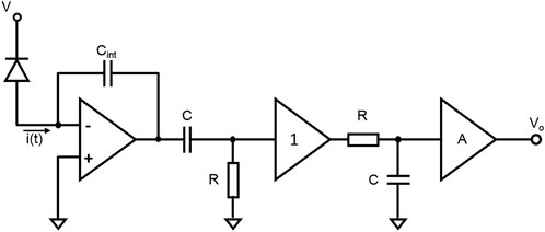
FIGURE 1. Typical setup for X-rays spectroscopy. The photo-generated current is integrated and the resulting signal is shaped by a CR-RC filter. A single photon generates a voltage pulse whose amplitude is proportional to the photon energy.
From Eq. 1 we see that high gain is beneficial in reducing the contribution of the noise of the read-out, but high gain must come with low associated noise, i.e., low F. The dark current should be as small as possible, otherwise the advantages related to high gain are hampered by the last term in Eq. 1.
The time constant of the CR-RC filter, as well as the duration of the time response of the APD itself, has to be small enough to ensure that two consecutive photons do not induce overlapping current waveforms. In fact, in this case the resulting output would no longer be proportional to the photon energy. Constraints on the maximum duration of the time response, as usual, translate into a demand for a large bandwidth of the APD.
Obtaining APDs with high M, low F, low Idark and high bandwidth is not an easy task and different device structures have been proposed with many combinations of materials. In particular, the detection of hard X-rays requires semiconductors with high atomic number since they possess a large stopping power, thus providing a larger quantum efficiency. For this reason, III-V compound semiconductors such as GaAs are a possible choice. Unfortunately, as we will discuss in the following, GaAs APDs feature a quite large F when trying to obtain high gains unless the intrinsic region is very narrow [14]. The use of superlattices of GaAs and AlGaAs improves noise [8]; [15]. In these latter devices the absorption region, where e-h pairs are generated by photon absorption, is separated by the region where II takes place (multiplication region), see Figure 2. This allows to separately optimize the dark current and the multiplication process. This structure will be referred as Separate-Absorption-and-Multiplication (SAM) APD.
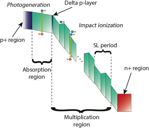
FIGURE 2. Sketch of the band-diagram of a SAM-APD. The absorption region (GaAs in the results reported in the following), where generation of e-h pairs by photon absorption occurs, is separated from the multiplication region (where impact ionization events take place) by a δ layer with p doping. The multiplication region consists of a superlattice.
It is evident that designing a complex structure like the one in Figure 2 requires adequate simulation approaches. Models for APDs range from the simple local model developed in the ’60s [16] up to sophisticated full-band Monte Carlo (FBMC) simulators [17]. However, the computational burden associated to FBMC simulations prevents their use for extensive device optimization, so that simpler approaches such as Non-Local/History Dependent (NLHD) models [18] as well as Random-Path-Length (RPL) algorithms [19] have been proposed. In this paper we describe a suite of modeling tools that includes a NLHD model for gain and noise as well as an RPL algorithm (based on the same effective field as in the NLHD model) to evaluate the time response of the APD in the presence of X-ray photons. A FBMC is employed to assess the most suitable form for the effective electric field to be used in the NLHD model. Comparison with experimental data for SAM-APDs featuring an AlGaAs/GaAs super-lattice in the multiplication region is also provided. We do not discuss here the modeling of the device electrostatics and of the dark current that is usually carried out with TCAD tools for electron devices (e.g. [20]).
The paper proceeds as follows. Existing impact ionization models for gain and noise in APDs are reviewed in Section 2. A NLHD model specifically developed for SAM-APDs with a staircase structure in the multiplication region is presented in Section 3 and compared with FBMC simulations as well as with experimental data. The improved RPL algorithm is detailed in Section 4. Conclusion are drawn in Section 5.
Impact ionization is a stochastic process where an electron in the conduction band gains enough kinetic energy to promote another electron from valence to conduction band after a scattering event, thus creating an additional electron-hole pair (similarly for hole initiated II). Proper modeling of such events requires a probabilistic approach usually based on Monte Carlo techniques. In fact, the probability per unit time for an electron to create an e-h pair depends on its energy, that in turn depends on the electric field profile experienced since its generation (by optical process or II) and on the sequence of scattering events suffered. Moreover, the energy distribution of the e-h pair and of the original electron after II also follows a stochastic distribution [21].
To significantly simplify the modeling of II, the local model assumes the impact ionization generation rate at position x and, thus, the electron and hole ionization coefficients (α(x) and β(x)) to depend only on the electric field at the same location x. By further assuming that the ratio k = β/α does not depend on the electric field, one can derive simple expressions for the gain and excess-noise [16] as well as for the bandwidth [22]. In particular, for the excess noise factor in the case of electron injection, one finds:
This expression is plotted in Figure 3 for different values of k.
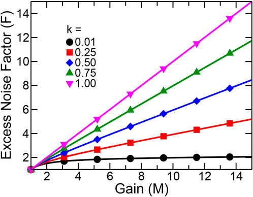
FIGURE 3. Excess noise factor as a function of the gain from the local model (Eq. 2) for k = 0.01, 0.25, 0.5, 0.75, 1.
The local model can provide precious indications about how the width of the multiplication region and the employed material affect multiplication and the associated noise. In particular, one can see in Figure 3 and in [22] that the best materials (providing higher bandwidth-gain product and lower excess noise) are the ones where electron initiated II significantly dominates over hole initiated process (i.e., where k is low). Silicon possesses k ≪ 1 (see Figure 4A) but the attenuation length in the energy range of X-rays is long (see Figure 4B), requiring thick absorption regions. GaAs instead has a k approaching 1 (that is detrimental for noise) but an attenuation length for X-ray photons much shorter than Si, suggesting a larger quantum efficiency for GaAs APDs.
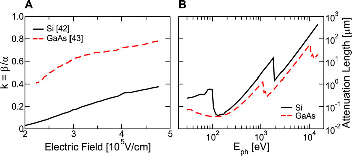
FIGURE 4. (A) Ratio between the hole and electron impact ionization coefficients for Si from [42] (black solid) and for GaAs from [43] (red dashed) at room temperature. (B) Attenuation length in Si (black solid) and in GaAs (red dashed) for photon energies in the range 30 ≤ Eph ≤ 15,000 eV from [44].
Experimental results for excess-noise vs. gain in GaAs p-i-n APDs with thin absorption regions points out a reduction of F for given M as the intrinsic region gets thinner [23]. Figure 5B shows that the local model cannot capture this effect, predicting essentially the same value of F for given M regardless of the thickness of the intrinsic region. The gain vs. applied voltage is however captured quite well (see Figure 5A).
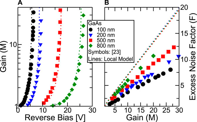
FIGURE 5. Comparison between the local II model and the experiments in [23] for GaAs p-i-n diodes with different width of the intrinsic region. Plot (A): gain vs. applied voltage. Plot (B): excess noise factor vs. gain. II ionization rates are taken from [26].
The limitations of the local model lead to the development of non-local/history dependent models [18]; [24]; [25]. In these models the II coefficients are not only a function of the ionization position x′ but also on the position x where the carrier was generated (by photon absorption or by II), i.e., one should write α(x|x′) and β(x|x′). Different models [18]; [24]; [25] assume different functional forms for α(x|x′) and β(x|x′) vs. the electric field profile, but all share the same set of equations relating α(x|x′) and β(x|x′) to gain and excess-noise. In particular for an e-h pair generated at position x, the gain is given by
with Ne(x) and Nh(x) being the average values of the number of carriers (ne(x) and nh(x)) generated by a chain of II events triggered by, respectively, an electron and a hole that were generated, either optically or by II, at position x. These are given by the following integral equations (assuming a multiplication region extending from x = 0 to x = W and electrons moving toward positive x, holes moving toward negative x):
where the survival probabilities (i.e., the probabilities that the primary carriers reach x′ from x without suffering impact ionization scattering) are given by:
In Eqs 4, 5, the first term is the probability that the primary carrier reaches the boundary of the multiplication region without suffering impact ionization scattering; on the other hand, the second term is the average number of ionization events that result from a first ionization that occurred anywhere between x and W, for electrons, or between 0 and x, for holes.
The excess noise factor is instead given by
where ⟨ne(x)2⟩ and ⟨nh(x)2⟩ are given by
We have shown in [25] that the two systems of integral equations (one formed by Eqs 4, 5, the other consisting in Eqs 9,10) can be turned into linear algebra problems after defining a suitable spatial mesh.
As said above, the different NLHD models proposed so far essentially differ in the way they formulate the expressions for α(x|x′) and β(x|x′). In the following, we will describe few of them reporting only the expression for α(x|x′) since the one for β(x|x′) is similar. The dead-space model [18] assumes that if the distance between the initial generation position x and the position where II takes place x′ is shorter than a minimum length de (the dead-space), the ionization probability is null, whereas it tends to a local expression otherwise, i.e.:
where
with Fx being the electric field and Eth,e a suitable threshold energy for II.
Figure 6 shows that the dead-space model (with the parameters taken from [26]) correctly predicts the reduction of the excess noise factor for a given gain that is experimentally measured in p-i-n APDs as the diode thickness shortens [23]. The trend in Figure 6A (i.e. the high gain in thin diodes for given bias and consequently lower breakdown voltage) can be explained by considering that in thin diodes large electric fields (i.e. large gains) can be obtained by applying small reverse bias voltages. On the other hand, the behavior of F(M) in Figure 6B is justified by the fact that, for a given electric field, the dead-space becomes comparable to the thickness of the active region of the diode as the latter reduces. Therefore, in thin diodes the presence of the dead space lowers the probability of having multiple impact ionization events, making the whole multiplication process more deterministic and, thus, lowering the associated noise.
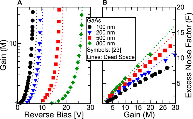
FIGURE 6. Comparison between the dead-space model and the experiments in [23] for GaAs p-i-n diodes with different width of the intrinsic region. Plot (A): gain vs. applied voltage. Plot (B): excess noise factor vs. gain.
The main problem of the dead-space model is that it is not clear how to define de in the presence of non-uniform electric field profiles. For example, in Figure 6 we used in Eq. 12 the average of the electric field between x and x′. This makes the model hard to apply to multiplication regions with conduction band discontinuities as the superlattices used in [27]. One should also notice that the local ionization coefficient (αloc) used in Eq. 11 differs from the ones extracted from experiments under uniform fields (αmeas) or, in other words, to the one that should be used in the local model. In fact, following [28]:
The model in [24] instead relates the II coefficient to an effective field:
where
similarly to the dead-space concept. The non-local II coefficients are then expressed as:
where Ae, Ece and γe (and similarly for holes) are suitable adjusting parameters to reproduce the M(V) and F(M) curves [24].
We recently proposed [25] a NLHD model similar to the one in [24], but replacing Eq. 14 with:
where Ec is the conduction band edge. This time λe is a parameter to be adjusted (together with Ae, Ece and γe and the corresponding parameters for holes) to reproduce M(V) and F(M) curves. Eq. 17 follows from the simple energy balance equation that can be derived from the second moment of the Boltzmann Transport Equation. For this reason the model will be referred as Energy Balance History Dependent Model (EBHDM). We have shown in [25] that the EBHDM reproduces the M(V) and F(M) curves for p-i-n APDs measured in [23] for different III-V compounds and alloys.
The expressions for the effective field require an electric field (or, better, a quasi field to account for band discontinuities) to be provided e.g., by commercial TCAD tools. In the APDs, working in linear mode, charge multiplication is kept under control and the generated charge has a negligible impact on the device electrostatics. As a result, a self-consistent coupling between electrostatic and carrier dynamics is not needed and the band profiles from TCAD can be kept frozen when modeling the II phenomena.
As a final remark to this section, one should consider that the model proposed here, as well as the ones in [18]; [24], is both non-local and history-dependent. Both aspects are relevant when studying multiplication and noise in APDs: a model that is non-local but is not history dependent would predict a gain different from the local model, but the relation between F and M would be very similar to the one in Figure 3 rather than to the experimental data for this APDs in Figure 6 (see [25]).
As discussed in the previous section, III-V compounds such as GaAs are promising in terms of quantum efficiency, but the noise associated to the multiplication process is high since electrons and holes have similar ionization probabilities. This has led to the proposal of using superlattices obtained by alternating layers with different conduction band edges (e.g., GaAs and AlGaAs as sketched in Figure 2) [29]. The conduction band discontinuities increase the electron ionization probability, while the valence band profile is engineered to have negligible discontinuities. As a results the factor k = β/α is significantly lowered. In addition, II is strongly localized and this further lowers the noise.
Clearly the local model is unable to handle such structures, so that specific models have been developed to predict the gain and excess noise. In particular, assuming that II takes place only at the band discontinuities and that only electrons ionize with probability 0 ≤ Pe ≤ 1, [29] proposed the following equations for gain and excess noise:
where Nstep is the number of periods of the superlattice. When Pe tends to 1 (we double the electrons after each conduction band discontinuity), the excess noise factor tends to 1. A generalization of Eqs 18, 19 for a structure with non-uniform steps has been proposed in [30].
In most material systems1, the conduction band discontinuities in the superlattice are not large enough to bring Pe close to 1 and an electric field resulting from the increase of the applied bias voltage has to be induced in the regions between consecutive steps to obtain significant carrier multiplication. The model in Eqs 18, 19 has been extended to include II between consecutive steps in [31]:
where Ph is the hole impact ionization probability in each layer computed using the local model:
and kp = Ph/Pe.
The non-local models described in Section 2 have been initially developed for p-i-n diodes and their applicability to superlattices with a staircase band structure is not obvious. For example, concerning the dead-space model, [32] introduced the concept of scattering aware ionization coefficients, assuming that a carrier becomes cold if it travels for a suitably-defined distance across a region with an electric field below a specific threshold. Without this workaround, the dead-space model would apply the dead-space only to the first period of the superlattice, treating the rest of the structure as local. The model in [24] (see Eqs 14, 15) features singularities when the quasi-electric field at the conduction band step tends to infinite. The singularity at the heterojunction in the model of [25] has been removed by proper discretization of the integral in Eq. 17 when approaching dEC/dx → ∞.
It can be demonstrated that the NLHD framework of Eqs 3–10 assuming electron II events localized at discrete coordinates (i.e., the conduction band steps) and no hole II exactly gives the gain and noise of Eqs 18, 19, see results in [25]. Direct comparison between Eqs 20–22 and the EBHDM of [25] has been provided in [33].
Although the NLHD framework can be applied to superlattices with staircase structure, it is not clear how accurate the specific models that link the NLHD II coefficients to the quasi electric field are. In other words, the validity of Eq. 11 (for the dead-space model) and of Eqs 17, 16 (for the model in [25]) needs to be assessed. For that purpose we have developed a Full-Band Monte Carlo (FBMC) simulator and devised a methodology to extract the α(x|x′) and β(x|x′) from the FBMC results for template structures [34]. Figures 7, 8 report sample results for a template structure consisting in a GaAs region with uniform applied electric field. In Figure 7 electrons are injected at x = 0 and holes at x = 500 nm with negligible initial kinetic energy. In Figure 8, instead, the GaAs region is placed after a conduction band step of amplitude ΔEC (i.e., carriers are injected at the contacts with initial kinetic energy equal to ΔEC). As it can be seen in both figures, the dead-space model has a kind of hard threshold that is not consistent with the FBMC results. On the other hand, the model in [25] predicts II events closer to the band edge compared to the FBMC.
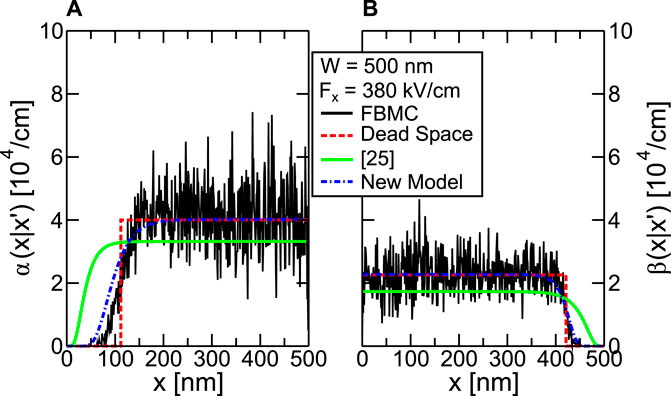
FIGURE 7. Comparison between the α(x|x′) and β(x|x′) profiles extracted from FBMC simulations using the methodology presented in [34] and different NLHD models (see text). The considered structure is a GaAs region of 500 nm width under a uniform electric field Fx = 380 kV/cm.
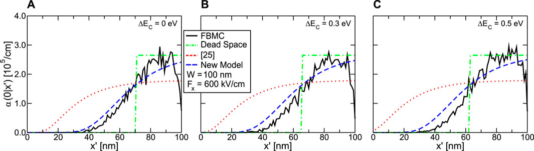
FIGURE 8. α(x, x′) profiles as in Fig.7 but for a GaAs region (100 nm of width) following energy steps of different amplitude ΔEC. A uniform electric field Fx = 600 kV/cm is present in the GaAs region.
We have thus investigated the limitations of Eq. 17 that has been derived from the second moment of the Boltzmann equation:
where w is the average carrier energy and w0 is the thermal energy at equilibrium. We see that λe can be extracted from FBMC simulations of uniform structures under constant electric field by plotting
Results for GaAs are reported in Figure 9 (crosses) and show that λe and λh are far from being constant. For that reason we have replaced Eq. 17 with
(similarly for holes), where
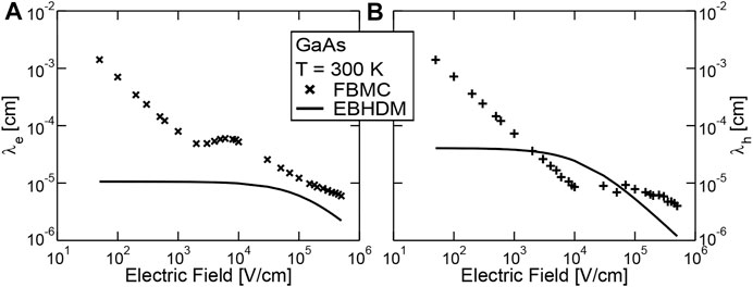
FIGURE 9. Dependence of the λe and λh parameters vs. the electric field. The crosses are the results of FBMC simulations of uniform GaAs regions under constant electric field where Eq. 24 is used to compute λe and λh from the average carrier energy. The lines are the best fits of Eq. 26 that makes the EBHDM reproduce the α(x′|x) and β(x′|x) from FBMC (examples in Figure 7).
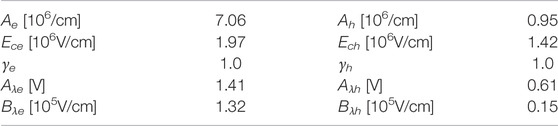
The blue dashed lines in Figure 7 show that the new model employing Eqs 25, 26 provides results quite close to the FBMC when the parameters Aλe,h and Bλe,h are chosen properly. The model parameters are summarized in Table 1. The parameters Ae, Ah, Ece, Ech, γe and γh required by Eq. 16 have been extracted from FBMC simulations similar to the ones in Figure 7 without the conduction band step but with different levels of electric fields by matching the α(x|x′) and β(x|x′) once they become independent on x′ (e.g., close to the right boundary of the simulation domain for electrons). On the other hand, Aλe,h and Bλe,h have been adjusted to match the whole shape of the α(x|x′) and β(x|x′) profiles.
The values of λe and λh from Eq. 26 using the parameters in Table 1 are reported by lines in Figure 9: we see that they differ from the values from Eq. 24, but this is reasonable since II is not related to the average carrier energy, but rather to the distribution of carriers with energy above the threshold for II. This would demand for a more complicated energy balance equation that is however beyond the scope of this work, since the empirical Eq. 26 works well in reproducing the FBMC results.
As a further test for the new model proposed in this section, we perform a direct comparison with experimental data. In particular, we consider APDs with the epitaxial structure sketched in Figure 2 that were grown by Molecular Beam Epitaxy on n+ GaAs (001) substrates. The multiplication region consists of a 12 times repetition of a GaAs/Al0.45Ga0.55As/AlxGa1−xAs (0.45 < x < 0) superlattice (35/25/20 nm) where the composition of the last layer is graded linearly through a digital alloy. A carbon δ-doped layer (p = 2.5 ⋅ 1012 cm−2) separates electrostatically the multiplication and the absorption regions. The latter is grown on top of the δ-doped layer and consists of a 4.5 μm-thick GaAs layer. The epitaxial structure is concluded by a 150 nm p+ GaAs (6 ⋅ 1018 cm−3) contact layer. Circular mesa diodes with diameters 200–600 μm were defined by optical photolithography and wet chemical etching. An Al2O3 passivation layer was e-beam-evaporated to reduce leakage currents. Concentric openings on the tops of the mesas were defined by lift off technique. Cr/Au p contacts and AuGe/Ni/Au n contacts were deposited on the top of the mesas, inside the openings of the dielectric, and on the back surface, respectively.
The fabricated devices were tested under light to assess their response to incoming photons, determining their gain and the noise induced by the multiplication process. For this characterization, in order to ensure that photogeneration took place entirely within the absorption region, a green (λ = 532 nm) tabletop laser has been used. In fact, in this energy range the absorption length is approximately 160 nm, which is much shorter than the absorption region. The response to photons was calculated as the difference between the dark and the photocurrent: the gain Mmeas was defined as the current normalized by its value at the highest voltage (V*) which guaranteed that the multiplicative process could not be started:
where the dark current Idark is essentially negligible for the illumination values considered here.
The excess noise factor is extracted as
that is the ratio between the actual noise of the APD current and the shot noise of photogenerated current passed through a noiseless multiplier device. The power spectral density of the noise current Sii has been measured with a customized trans-impedance amplifier (TIA) whose schematics is depicted in Figure 10. It can be seen that the signal amplified by the TIA, characterized by a high cutoff frequency (11 MHz), is fed through a decoupling capacitor into a signal analyzer (Agilent EXA N9010A) which registers the Sii value as the reverse bias voltage increases. The value inserted into Eq. 28 is an average between the values measured between 1.5 and 2 MHz.
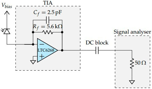
FIGURE 10. Schematic of the dedicate trans-impedance amplifier used to measure the power spectral density of the noise current.
Figure 11 reports the experimental gain vs. voltage 1) and excess noise factor vs. gain 2) and compare them with the results of the EBHDM. The model parameters in Table 1 have been used without any adjustment. The breakdown voltage is underestimated by the model, while the excess noise factor is nicely reproduced. Consider that in the model AlGaAs has been treated as GaAs, that may explain the lower breakdown (due to smaller gap of GaAs w.r.t. AlGaAs).
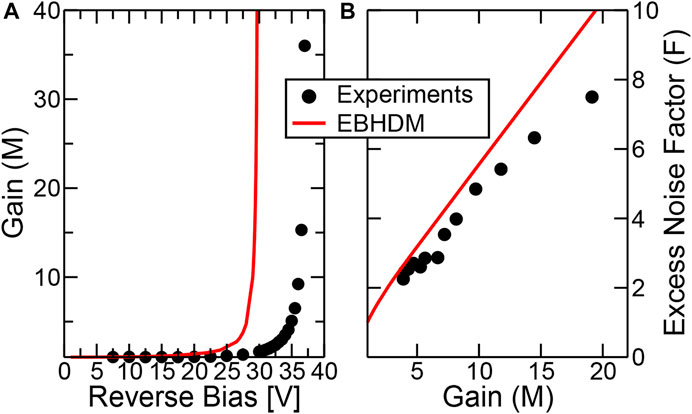
FIGURE 11. Comparison between experimental gain vs. voltage (A) and excess noise factor vs. gain (B) and simulations using the EBHDM with variable λe and λh.
The experimental F-M curves in Figure 11. b are close to the results of the local model of Eq. 2 with k = 0.3 meaning that the presence of the superlattice has significantly increased electron II compared to hole II, since in bulk GaAs one would expect a value of k as high as 0.8 (see Figure 4A).
Modeling the response of the APD after a photon is detected is significantly more complicated than estimating M and F as described above. In principle FBMC simulations, being inherently time dependent, may provide the current waveforms, but these simulations are extremely time consuming when considering structures as in Figure 2.
The non-local models presented in Section 2 can be extended to become time dependent, as shown in [35] for the dead-space model and in [24] for the model based on effective fields. These models are however hardly applicable to SAM-APDs.
A viable alternative to efficiently compute the time response of an APD is the Random-Path-Length (RPL) algorithm. It has been initially proposed for p-i-n APDs where the electric field is essentially constant inside the structure [19]; [36]. We start describing the algorithm under these conditions and only later move to its application to SAM-APDs as in Figure 2.
The RPL is essentially a Monte Carlo algorithm based on the fact that the survival probability (i.e., the probability not to ionize) between x and x′ defined in Eq. 6 has an uniform distribution, i.e.
where r is a random number uniformly distributed between 0 and 1. Similarly for Psh. Considering the dead space model and a constant electric field, substitution of Eq. 11 into Eq. 29 gives
In other words, if an ionization event for a given electron takes place at x, the next one takes place at a random position x′ computed inserting a random number uniformly distributed between 0 and 1 into Eq. 30. Each ionization event creates an e-h pair and the two carriers are simulated until they exit the simulation domain. According to Ramo’s theorem (see for example [37]), the movement of the electron between x and x′ induces a current pulse of time duration (x′ − x)/ve (where ve is the electron velocity, assumed to be equal to the high-field saturation velocity) and amplitude qve/W, where W is the width of the intrinsic region. Combining the pulses induced by all carriers one gets the time response of the APD to a photon that impinged at a given position.
In [38] we have shown that the RPL algorithm can be applied to any functional form of α(x, x′), focusing on the model in [25] (i.e., Eq. 16 plus Eq. 17). This implies also that arbitrary electric field profiles can be handled. Equation 29, in principle, should be solved when computing every single new x′ position. The problem has been solved by storing in a look-up table the Pse for each value of x and x′. The x and x′ spacing is small enough to produce discretization-independent results. Then for a given x and r, a binary search is performed in the table to find the value of x′ that satisfies the relation. A similar methodology is used to describe the motion of holes. As described in [38], each time a carrier ionizes, the algorithm recursively simulates the motion of the electron and hole originated from the parent carrier, until they are collected by the contacts, then it goes back to the simulation of the parent carrier.
In [38] we have also shown that if different trials are run for pairs generated at the same position x and for each of them a gain mi is found, the RPL can be used to compute M = ⟨mi⟩ and
As said before, the original RPL algorithm of [19]; [36] as well as the extension in [38] work for p-i-n diodes. An improved RPL model for SAM-APDs has been presented in [39]. Although the treatment of II in the multiplication region remains almost the same, the improved model has two main additional features. First of all, the generalized Ramo’s theorem of [40] is employed to compute the current pulse associated to the movements of the carriers between x and x′. In fact the formulation in [40] is able to handle partially depleted structures: while in a p-i-n diode the carrier moving in the intrinsic region induces charge at the boundary of the region itself, in the case of SAM-APDs the absorption region is entirely modulated by the charge induced by carriers moving there or in the multiplication region. This leads to formulas much more complicated to the well-known form of Ramo’s theorem. The interested reader can find the complete expressions in [40]; [39]. The second additional feature is the inclusion of Monte Carlo transport into the absorption region. In this region, the electric field is very low and II does not take place. Furthermore, ve is not constant as in the multiplication region. Carriers are thus moved with free-flight with random time duration
where μ(x) is the effective mobility at position x (it can be extracted from the same TCAD simulation that provide the electric field profile) and meff a suitable effective mass (more details in [39]). After the free-flight, the velocity of the particle is randomized according to a Normal distribution with zero mean and variance equal to the thermal velocity
In this paper we improve the simulation framework proposed in [39] by using for the non-local II coefficient the expression based on the effective field with variable λe, see Eq. 25, that has been verified by comparison with FBMC simulations in Section 3. A typical simulation run consists in many trials, each one corresponding to the absorption of a photon. A single trial proceeds as follows:
1. the photon is absorbed at a random position inside the device based on the attenuation length corresponding to the photon energy;
2. N e-h pairs are generated according to a Normal distribution with mean
3. the generated carriers move into the absorption regions with free-flight with duration according to Eq. 31, while in the multiplication region they follow the RPL algorithm;
4. a single trial ends when all generated carriers (the initial N pairs generated by the photon as well as the other pairs generated by II by the RPL algorithm) exit the device;
5. during carrier transport, current at the terminals is computed according to the generalized Ramo’s theorem [40].
The model thus accounts for many sources of randomness in the process of X-ray detection: random position for absorption, random number of generated e-h pairs, random motion of charges in the absorption region, random process for charge multiplication.
Sample waveforms resulting for a few trials are reported in Figure 12. Due to the high photon energy (that implies generation of a large number of e-h pairs following photon absorption), here the main source of randomness is the position where the photon is absorbed. On the other hand, the random motion of carriers and their multiplication is averaged out during each trial. We have in fact verified that trials corresponding to photons absorbed in the same position produces waveforms that are very similar in shape and amplitude. Time responses for APDs as those described in Section 3 have been measured in [41]. A 1:1 comparison with the simulation in Figure 12 is not possible due to the effects of the read-out parasitics and the fact that the fabrication process was not as mature as for the results shown in Figure 11. A deeper analysis of the time response, thoughtfully comparing experiments and models will be carried out in a future work.
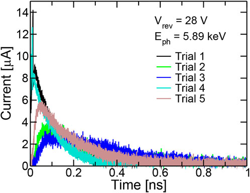
FIGURE 12. Sample waveforms (absorption of photons with energy 5.89 keV) obtained with the RPL algorithm for a SAM-APD with a structure as in Figure 2. At the considered bias, the gain is M = 4.7 and the excess noise factor is F = 3.05.
From the current waveforms one can determine the Power Spectral Density of the current noise of the APD as
where Λ is the rate of photon absorption and
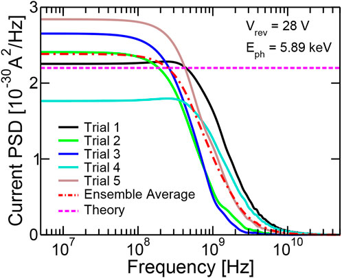
FIGURE 13. Power spectral density of the waveforms in Figure 12 computed using Eq. 32. They are normalized to a photon absorption rate Λ = 1 Hz. The theoretical value of the low frequency value from Eq. 34 is reported by the dashed line.
When considering absorption of photons in the visible range (i.e., generating one e-h pair per photon), the theoretical value of Sii is
This has been verified in [39] by computing Sii inserting into Eq. 32 the waveforms from the RPL algorithm. When dealing with X-rays, instead, the fact that one photon generates many e-h pairs can be interpreted as an additional multiplication step at the beginning of the structure having gain N = Eph/Eehp and excess noise factor Fp = 1 + f/N. By employing the formula proposed in [30] to combine the multiplication steps, one find that for X-rays the current noise has a Power Spectral Density:
We have presented a suite of modeling approaches to determine the performance of APDs for X-rays detection. They can be summarized with the help of Figure 14. The FBMC is the most accurate approach, but hardly applicable to a complex structure with many conduction band steps and extending for many microns that need to be simulated for times in the nanosecond range, mainly because of the associated computational burden. On the other hand, the FBMC is very powerful as a tool to verify and calibrate the expressions for the non-local II parameters (as done in this work in Figures 7, 8). The resulting expressions for α(x| x′) and β(x| x′) are then used in the RPL algorithm (that is able to efficiently compute the current waveforms for devices some micrometers long and over time scales of nanoseconds) or in a NLHD model such as the EBHDM to obtain gain and noise. The RPL can in principle provide the same information as the EBHDM, but requires the simulation of many trials, whereas the EBHDM directly solves the equations providing gain and noise that are needed to estimate the energy resolution of the detection system.
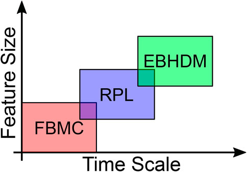
FIGURE 14. Schematic representation of different simulation approaches for II in APDs. Each model is suited to analyze different feature sizes and time scales.
Notice that our focus here was on the performance related to the multiplication process. Relevant figures of merits such as the dark current are not addressed here.
The same simulation framework presented here can be in principle applied also to the detection of γ-rays by adding a model for the generation of the fluorescent photons in the scintillator coupled to the APD.
The raw data supporting the conclusion of this article will be made available by the authors, without undue reservation.
All authors contributed to conception and design of the study. Model development and software: AP, CN, DE, FR, LS, and PP. Device Fabrication: GB, TS, and CN. Experimental: FA, MA, GC, MCa, MCo, FD, and RM. Funding: FA, GB, GC, and PP. AP and PP wrote the first draft of the manuscript. All authors contributed to manuscript revision, read, and approved the submitted version.
This work was supported by the Italian MIUR through the PRIN 2015 Project under Grant 2015WMZ5C8.
The authors declare that the research was conducted in the absence of any commercial or financial relationships that could be construed as a potential conflict of interest.
All claims expressed in this article are solely those of the authors and do not necessarily represent those of their affiliated organizations, or those of the publisher, the editors and the reviewers. Any product that may be evaluated in this article, or claim that may be made by its manufacturer, is not guaranteed or endorsed by the publisher.
1An exception being InAs compounds and alloys (see for example [45]) that however are not relevant for X-ray detection.
1. Renker D. Geiger-mode Avalanche Photodiodes, History, Properties and Problems. Nucl Instr Methods Phys Res Section A: Acc Spectrometers, Detectors Associated Equipment (2006) 567:48–56. doi:10.1016/j.nima.2006.05.060
2. Spanoudaki VC, Levin CS. Photo-detectors for Time of Flight Positron Emission Tomography (ToF-PET). Sensors (2010) 10:10484–505. doi:10.3390/s101110484
3. Powolny F, Auffray E, Brunner SE, Garutti E, Goettlich M, Hillemanns H, et al. Time-based Readout of a Silicon Photomultiplier (SiPM) for Time of Flight Positron Emission Tomography (TOF-PET). IEEE Trans Nucl Sci (2011) 58:597–604. doi:10.1109/tns.2011.2119493
4. Agishev R, Comerón A, Bach J, Rodriguez A, Sicard M, Riu J, et al. Lidar with SiPM: Some Capabilities and Limitations in Real Environment. Opt Laser Tech (2013) 49:86–90. doi:10.1016/j.optlastec.2012.12.024
5. Akiba M, Inagaki K, Tsujino K. Photon Number Resolving SiPM Detector with 1 GHz Count Rate. Opt Express (2012) 20:2779–88. doi:10.1364/OE.20.002779
6. Liu J, Kucharczyk K, Lutchman R, Donetski D. Progress toward Soft X-ray Beam Position Monitor Development. In: 12th International Particle Accelerators Conference IPAC2021 (2021).
7. Chee Hing Tan CH, Gomes RB, David JPR, Barnett AM, Bassford DJ, Lees JE, et al. Avalanche Gain and Energy Resolution of Semiconductor X-ray Detectors. IEEE Trans Electron Devices (2011) 58:1696–701. doi:10.1109/TED.2011.2121915
8. Lauter J, Protić D, Förster A, Lüth H. AlGaAs/GaAs SAM-Avalanche Photodiode: An X-ray Detector for Low Energy Photons. Nucl Instr Methods Phys Res Section A: Acc Spectrometers, Detectors Associated Equipment (1995) 356:324–9. doi:10.1016/0168-9002(94)01237-7
9. Gomes RB, Tan CH, Lees JE, David JPR, Ng JS. Effects of Dead Space on Avalanche Gain Distribution of X-ray Avalanche Photodiodes. IEEE Trans Electron Devices (2012) 59:1063–7. doi:10.1109/TED.2012.2182674
10. Campbell JC. Recent Advances in Avalanche Photodiodes. J Lightwave Technol (2016) 34:278–85. doi:10.1109/JLT.2015.2453092
11. Ren M, Maddox S, Chen Y, Woodson M, Campbell JC, Bank S. AlInAsSb/GaSb Staircase Avalanche Photodiode. Appl Phys Lett (2016) 108:081101–4. doi:10.1063/1.4942370
12. Nada M, Nakajima F, Yoshimatsu T, Nakanishi Y, Tatsumi S, Yamada Y, et al. High-speed III-V Based Avalanche Photodiodes for Optical Communications-The Forefront and Expanding Applications. Appl Phys Lett (2020) 116:140502. doi:10.1063/5.0003573
13. Gatti E, Manfredi PF. Processing the Signals from Solid-State Detectors in Elementary-Particle Physics. Riv Nuovo Cim (1986) 9(1978-1999):1–146. doi:10.1007/BF02822156
14. Yuan P, Hansing CC, Anselm KA, Lenox CV, Nie H, Holmes AL, et al. Impact Ionization Characteristics of III-V Semiconductors for a Wide Range of Multiplication Region Thicknesses. IEEE J Quan Electron. (2000) 36:198–204. doi:10.1109/3.823466
15. Gomes RB, Tan CH, Meng X, David JPR, Ng JS. GaAs/Al0.8Ga0.2As Avalanche Photodiodes for Soft X-ray Spectroscopy. J Inst (2014) 9:P03014. doi:10.1088/1748-0221/9/03/p03014
16. McIntyre RJ. Multiplication Noise in Uniform Avalanche Diodes. IEEE Trans Electron Devices (1966) ED-13:164–8. doi:10.1109/T-ED.1966.15651
17. Dolgos D, Meier H, Schenk A, Witzigmann B. Full-band Monte Carlo Simulation of High-Energy Carrier Transport in Single Photon Avalanche Diodes: Computation of Breakdown Probability, Time to Avalanche Breakdown, and Jitter. J Appl Phys (2011) 110:084507. doi:10.1063/1.3652844
18. Hayat MM, Sargeant WL, Saleh BEA. Effect of Dead Space on Gain and Noise in Si and GaAs Avalanche Photodiodes. IEEE J Quan Electron. (1992) 28:1360–5. doi:10.1109/3.135278
19. Ong DS, Li KF, Rees GJ, David JPR, Robson PN. A Simple Model to Determine Multiplication and Noise in Avalanche Photodiodes. J Appl Phys (1998) 83:3426–8. doi:10.1063/1.367111
21. Fischetti MV, Laux SE. Monte Carlo Analysis of Electron Transport in Small Semiconductor Devices Including Band-Structure and Space-Charge Effects. Phys Rev B (1988) 38:9721–45. doi:10.1103/PhysRevB.38.9721
22. Emmons RB. Avalanche‐Photodiode Frequency Response. J Appl Phys (1967) 38:3705–14. doi:10.1063/1.1710199
23. Yuan P, Anselm KA, Hu C, Nie H, Lenox C, Holmes AL, et al. A New Look at Impact Ionization-Part II: Gain and Noise in Short Avalanche Photodiodes. IEEE Trans Electron Devices (1999) 46:1632–9. doi:10.1109/16.777151
24. McIntyre RJ. A New Look at Impact Ionization-Part I: A Theory of Gain, Noise, Breakdown Probability, and Frequency Response. IEEE Trans Electron Devices (1999) 46:1623–31. doi:10.1109/16.777150
25. Nichetti C, Pilotto A, Palestri P, Selmi L, Antonelli M, Arfelli F, et al. An Improved Nonlocal History-dependent Model for Gain and Noise in Avalanche Photodiodes Based on Energy Balance Equation. IEEE Trans Electron Devices (2018) 65:1823–9. doi:10.1109/TED.2018.2817509
26. Saleh MA, Hayat MM, Sotirelis PP, Holmes AL, Campbell JC, Saleh BEA, et al. Impact-ionization and Noise Characteristics of Thin III-V Avalanche Photodiodes. IEEE Trans Electron Devices (2001) 48:2722–31. doi:10.1109/16.974696
27. Lauter J, Forster A, Luth H, Muller KD, Reinartz R. AlGaAs/GaAs Avalanche Detector Array-1 GBit/s X-ray Receiver for Timing Measurements. IEEE Trans Nucl Sci (1996) 43:1446–51. doi:10.1109/23.507080
28. Jeng Shiuh Cheong JS, Hayat MM, Xinxin Zhou X, David JPR. Relating the Experimental Ionization Coefficients in Semiconductors to the Nonlocal Ionization Coefficients. IEEE Trans Electron Devices (2015) 62:1946–52. doi:10.1109/TED.2015.2422789
29. Capasso F, Won-Tien Tsang W-T, Williams GF. Staircase Solid-State Photomultipliers and Avalanche Photodiodes with Enhanced Ionization Rates Ratio. IEEE Trans Electron Devices (1983) 30:381–90. doi:10.1109/T-ED.1983.21132
30. Pilotto A, Palestri P, Selmi L, Antonelli M, Arfelli F, Biasiol G, et al. A New Expression for the Gain-Noise Relation of Single-Carrier Avalanche Photodiodes with Arbitrary Staircase Multiplication Regions. IEEE Trans Electron Devices (2019) 66:1810–4. doi:10.1109/TED.2019.2900743
31. Teich M, Matsuo K, Saleh B. Excess Noise Factors for Conventional and Superlattice Avalanche Photodiodes and Photomultiplier Tubes. IEEE J Quan Electron. (1986) 22:1184–93. doi:10.1109/JQE.1986.1073137
32. Williams GM, Compton M, Ramirez DA, Hayat MM, Huntington AS. Multi-Gain-Stage InGaAs Avalanche Photodiode with Enhanced Gain and Reduced Excess Noise. IEEE J Electron Devices Soc (2013) 1:54–65. doi:10.1109/JEDS.2013.2258072
33. Pilotto A, Nichetti C, Palestri P, Selmi L, Antonelli M, Arfelli F, et al. Optimization of GaAs/AlGaAs Staircase Avalanche Photodiodes Accounting for Both Electron and Hole Impact Ionization. Solid-State Elect (2020) 168:107728. doi:10.1016/j.sse.2019.107728.Special
34. Pilotto A, Driussi F, Esseni D, Selmi L, Antonelli M, Arfelli F, et al. Full-Band Monte Carlo Simulations of GaAs P-I-N Avalanche Photodiodes: What Are the Limits of Nonlocal Impact Ionization Models? In: 2020 International Conference on Simulation of Semiconductor Processes and Devices (SISPAD) (2020).
35. Hayat MM, Saleh BEA. Statistical Properties of the Impulse Response Function of Double-Carrier Multiplication Avalanche Photodiodes Including the Effect of Dead Space. J Lightwave Technol (1992) 10:1415–25. doi:10.1109/50.166785
36. Ng JS, Tan CH, Ng BK, Hambleton PJ, David JPR, Rees GJ, et al. Effect of Dead Space on Avalanche Speed [APDs]. IEEE Trans Electron Devices (2002) 49:544–9. doi:10.1109/16.992860
37. Hamel L-A, Julien M. Generalized Demonstration of Ramo's Theorem with Space Charge and Polarization Effects. Nucl Instr Methods Phys Res Section A: Acc Spectrometers, Detectors Associated Equipment (2008) 597:207–11. doi:10.1016/j.nima.2008.09.008
38. Pilotto A, Palestri P, Selmi L, Antonelli M, Arfelli F, Biasiol G, et al. An Improved Random Path Length Algorithm for P-I-N and Staircase Avalanche Photodiodes. Int Conf Simulation Semiconductor Process Devices (Sispad) (20182018) 26–30. doi:10.1109/SISPAD.2018.8551751
39. Rosset F, Pilotto A, Selmi L, Antonelli M, Arfelli F, Biasiol G, et al. A Model for the Jitter of Avalanche Photodiodes with Separate Absorption and Multiplication Regions. Nucl Instr Methods Phys Res Section A: Acc Spectrometers, Detectors Associated Equipment (2020) 977:164346. doi:10.1016/j.nima.2020.164346
40. Riegler W. An Application of Extensions of the Ramo-Shockley Theorem to Signals in Silicon Sensors. Nucl Instr Methods Phys Res Section A: Acc Spectrometers, Detectors Associated Equipment (2019) 940:453–61. doi:10.1016/j.nima.2019.06.056
41. Nichetti C, Steinhartova T, Antonelli M, Cautero G, Menk RH, Pilotto A, et al. Gain and Noise in GaAs/AlGaAs Avalanche Photodiodes with Thin Multiplication Regions. J Inst (2019) 14:C01003. doi:10.1088/1748-0221/14/01/c01003
42. Van Overstraeten R, De Man H. Measurement of the Ionization Rates in Diffused Silicon P-N Junctions. Solid-State Elect (1970) 13:583–608. doi:10.1016/0038-1101(70)90139-5
43. Bulman GE, Robbins VM, Brennan KF, Hess K, Stillman GE. Experimental Determination of Impact Ionization Coefficients in. IEEE Electron Device Lett (1983) 4:181–5. doi:10.1109/EDL.1983.25697
44. Henke BL, Gullikson EM, Davis JC. X-ray Interactions: Photoabsorption, Scattering, Transmission, and Reflection at E = 50-30,000 eV, Z = 1-92. At Data Nucl Data Tables (1993) 54:181–342. doi:10.1006/adnd.1993.1013
Keywords: avalanche photodiodes, X-rays, modeling, Monte Carlo method, noise
Citation: Pilotto A, Antonelli M, Arfelli F, Biasiol G, Cautero G, Cautero M, Colja M, Driussi F, Esseni D, Menk RH, Nichetti C, Rosset F, Selmi L, Steinhartova T and Palestri P (2022) Modeling Approaches for Gain, Noise and Time Response of Avalanche Photodiodes for X-Rays Detection. Front. Phys. 10:944206. doi: 10.3389/fphy.2022.944206
Received: 14 May 2022; Accepted: 16 June 2022;
Published: 30 August 2022.
Edited by:
Coralie Neubüser, University of Trento, ItalyReviewed by:
Jiaguo Zhang, Paul Scherrer Institut (PSI), SwitzerlandCopyright © 2022 Pilotto, Antonelli, Arfelli, Biasiol, Cautero, Cautero, Colja, Driussi, Esseni, Menk, Nichetti, Rosset, Selmi, Steinhartova and Palestri. This is an open-access article distributed under the terms of the Creative Commons Attribution License (CC BY). The use, distribution or reproduction in other forums is permitted, provided the original author(s) and the copyright owner(s) are credited and that the original publication in this journal is cited, in accordance with accepted academic practice. No use, distribution or reproduction is permitted which does not comply with these terms.
*Correspondence: P. Palestri , cGllcnBhb2xvLnBhbGVzdHJpQHVuaXVkLml0
Disclaimer: All claims expressed in this article are solely those of the authors and do not necessarily represent those of their affiliated organizations, or those of the publisher, the editors and the reviewers. Any product that may be evaluated in this article or claim that may be made by its manufacturer is not guaranteed or endorsed by the publisher.
Research integrity at Frontiers
Learn more about the work of our research integrity team to safeguard the quality of each article we publish.