 M. Menichelli
 L. Servoli
 N. Wyrsch
95% of researchers rate our articles as excellent or good
Learn more about the work of our research integrity team to safeguard the quality of each article we publish.
Find out more
REVIEW article
Front. Phys. , 04 October 2022
Sec. Radiation Detectors and Imaging
Volume 10 - 2022 | https://doi.org/10.3389/fphy.2022.943306
Hydrogenated amorphous silicon (a-Si:H) particle detectors have been considered as alternatives to crystalline silicon detectors (c-Si) in high radiation environments, due to their excellent radiation hardness. However, although their capability for particle flux measurement in beam monitoring applications is quite satisfactory, their minimum ionizing particle (MIP) detection has always been problematic because of the poor signal-to-noise ratio caused by a low charge collection efficiency and relatively high (compared to crystalline silicon) leakage current. In this article, after a review of the status of technological research for a-Si:H detectors, a perspective view on MIP detection and beam flux measurements with these detectors will be given.
Hydrogenated amorphous silicon (a-Si:H) is a disordered semiconductor material that was initially investigated in 1969 by Chittik, Alexander, and Sterling [1]. This material was synthesized by radio‐frequency glow discharge from silane gas onto substrates. In 1976, a-Si:H was successfully doped by adding phosphine (for n-type material) or diborane (for p-type) to the gas mixture of hydrogen and silane during the glow-discharge deposition process [2]. This opened up the possibility of using this material for electronic components, solar cells, and particle detectors.
The lack of long-range order in the atomic structure of amorphous silicon (a-Si) has the consequence that not all Si–Si bonds can be saturated, and therefore dangling bonds (DBs) are present in this disordered material. Hydrogen is thus introduced into the material to passivate those DBs that behave as defects and recombination centers. The hydrogen concentration in the material has an impact on its bandgap, ranging from 1.7 to 1.9 eV (see [3] and references therein). A higher hydrogen content results in a larger bandgap. The bandgap also depends on the temperature during deposition. The typical hydrogen content of a-Si:H deposited by plasma enhanced chemical vapor deposition (PECVD), which is the most frequently used process for device quality material, is in the order of 10% atomic. In PECVD, a-Si:H material is generally deposited at temperatures around 200–250°C. Due to this relatively low temperature, a-Si:H layers can be deposited on a wide variety of substrates [4]. A non-exhaustive list of materials where a-Si:H can be deposited can be found in Ref. [5]. Detector-grade a-Si:H can be deposited with various techniques, such as PECVD with plasma excitation at radio frequency (13.56 MHz) [6], at very high frequency (VHF; 27–150 MHz) [7] or at microwave frequencies [8], and the well-established hot-wire chemical vapor deposition (HWCVD) [9]. A recent effort is ongoing to deposit a-Si:H using pulsed laser deposition (PLD) [5].
As previously mentioned, doping can be achieved by adding the doping agent to the silane-hydrogen mixture (or ablated Si and hydrogen mixture for PLD). Doping reduces the resistivity of the intrinsic material (in the order of 1010–1011 Ω cm for detector-grade undoped material) down to 10–100 Ω cm. However, doping also introduces many additional defects, and for this reason direct p-n junction cannot be used as active material in particle detectors and solar cells. Therefore, the simplest detector structures that have been fabricated and successfully tested are p-i-n diodes or Schottky diodes [10].
Recently, a-Si:H radiation sensors have become attractive thanks to the high level of radiation hardness of this material, which was first recognized in the framework of solar cell development for space applications. A comprehensive review of radiation damage tests performed on solar cells has been reported in Ref. [11]. In these studies, efficiency loss for total ionizing dose only becomes relevant (>10% loss) above 100 Mrad; while for displacement damage, the same efficiency loss is obtained at about 1015 neq/cm2. The authors also discuss the beneficial effect of annealing at temperatures in the range of 70°–130°C. They also make a comparison between various materials for solar cell fabrication (c-Si, GaAs, InP, and a-Si:H). The results shows that if the cells are operated at 70°C, with the combined effect of radiation and annealing, the efficiency of the a-Si:H cells is basically unchanged for a 2,800 km altitude orbit for a 10-year mission. This is about a factor 2 better than the other cells built with the previously mentioned materials. Radiation hardness studies have also been performed for a-Si:H photodiodes [12]. Photodiodes irradiated with 60Co gamma rays up to a dose of 2 Mrad showed an increase of leakage current by a factor ≈5. Afterward, 11 days storage at 22°C caused an auto-annealing process that decreased this increment down to a factor ≈2.5. An additional 1 Mrad of gamma ray irradiation then brought the increase in leakage current up to a factor 6 from the original value. Subsequent annealing for 21 days led to a linear reduction of the leakage current by a factor of 65%; and with an additional 21 days of annealing, to a reduction of 75% of the value just after irradiation. In conclusion, auto-annealing has to be considered as an important factor for the reduction of leakage current in beam measurement mode (as will be discussed later on).
Another important example of irradiation during beam monitoring applications is described by Wyrsch et al. [13]. In this application, a 32 µm thick diode was irradiated up to the fluence of 2 × 10¹⁶ protons/cm2 at the IRRAD1 facility at CERN with 24 GeV protons. Figure 1A shows the current induced by the proton beam at various fluencies. Because the beam had a constant rate (1.3 × 10¹¹ protons per spill), a constant current was expected in the absence of degradation. What is observed is a degradation of the current with expected saturation at 1015 p/cm2 (value extrapolated from current data) at a current value that is about 50% of the initial value. In this case, it is also possible to observe an example of auto-annealing process when, at the fluence of 4.5 × 10¹⁴ p/cm2, the beam was stopped for 20 h while the detector was kept under bias. A visible increase of the current when the beam was switched on was measured, which demonstrates the partial recovery of charge collection efficiency during the 20 h of annealing. Figure 1B shows the leakage current measurements at various stages of the irradiation and further annealing at 100°C for 12 and 24 h. It can be observed that after 24 h of annealing, the leakage current returns to original value before the irradiation. In the case of electron irradiation, metastable defects are created that can be completely removed by the annealing [14]. Noted that there is a lack of radiation testing with electrons above 1 MeV.
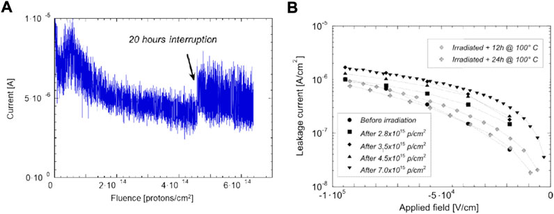
FIGURE 1. (A) Detector current versus proton fluence in a 32 µm thick a-Si:H p-i-n sensor at constant dose rate (1.3 × 10¹¹ protons/spill, 300 V bias) at 4.5 × 10¹⁴ protons/cm2 there was a 20 h beam interruption, where the effect of auto-annealing can be noticed. (B) Leakage current versus applied field in the same detector at various fluencies and after 12 and 24 h of annealing at 100°C and 300 V bias [13].
Many different kinds of particles have been detected using planar diode devices, including MIPs [10], x-rays [15], neutrons using both boron [16] or gadolinium converters [17], alpha particles [18], and heavier ions [19].
Despite the high radiation hardness of the resulting detectors, the use of these devices for MIP and x-rays has always been troublesome because of the poor S/N ratio resulting from the high leakage current at high depletion voltage and the low charge collection efficiency related with the defects in the material. The S/N ratio for MIPs using basic planar structures was in the order of 2–3.
The direct deposition of the detector on the readout application specific integrated circuit (ASIC) has been suggested as a possible solution for this problem. This approach, which is named thick film on ASIC (TFA), was used for the first time for visible light detection [20] and was then adopted for MIP detection using Niobium and Strontium beta sources. Figures 2A,B show the detector connection scheme of the readout electronics.
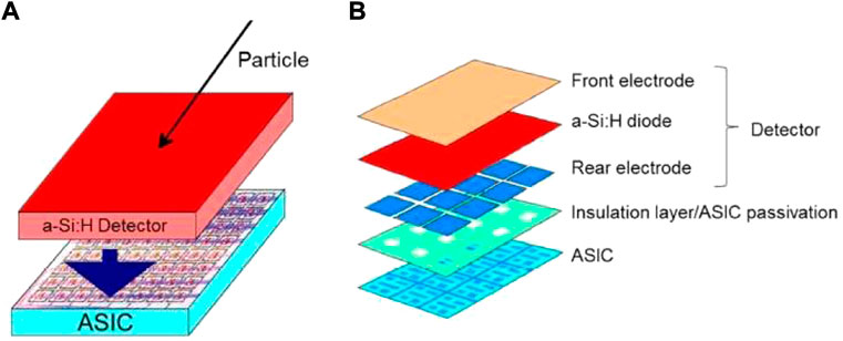
FIGURE 2. (A) Schematic design of integration of planar detector with the readout chip. (B) Exploded view of the detector plus readout chip assembly.
During the development of TFA sensors, the dependence of the performance on the shape of pixel was investigated. For this purpose, a test chip was designed at CERN to study this effect [21]. This chip included pixels of different sizes and shapes, micro-strips of various width and pitch distances, and has two different options for the openings in the ASIC passivation layer. The readout contact of the individual channels was provided by the signal readout metal layer of the ASIC through openings in the ASIC passivation. These openings can be local (single pixel) or global (group of pixels or the entire chip). The local openings can be a little larger or smaller than the pads. For TFA imagers, the edges of the passivation openings usually lead to a large additional surface leakage current. Therefore, a global opening was selected to lower leakage current values [22]. Diodes without an n-layer (i.e., an i-p layer structure deposited directly on the metallic back contact, metal-i-p configuration) were successfully tested for further reduction of the leakage current [23].
The same ASIC was also used to study spatial resolution and charge spread diffusion using microstrip configurations. The TFA detector was tested with electrons using electron-beam-induced current (EBIC) measurements and lateral charge collection spread was studied. The results of this test are shown in Figure 3 for a set of micro-strips (1.5 μm wide and spaced by 3.5 μm) on a 5 μm thick a-Si:H n-i-p diode. From this figure, it is evident that the signals from the strips are clearly separated because the lateral charge spread is in the order of few microns [10]. Cross talk (i.e., induced signal in neighbor strips) has been measured in another experiment with a beta source and was found to be negligible [22].
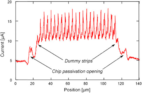
FIGURE 3. Signal from a set of microstrip 1.5 μm wide and spaced by 3.5 μm. Measurement was performed with an electron beam, bias voltage the detector was 30 V and beam energy was 20 keV.
In summary, spatial resolution in a-Si:H position detector (either strips or pixel) is determined only by the size and shape of the electrodes, and not by charge sharing (as it is on c-Si detectors). This enables this type of device to be used as high space resolution particle and x-ray detectors with very little dead-space.
Unfortunately, even with the TFA approach, the maximum S/N ratio for MIPs was around 5. Although this is better than the previous results obtained with planar detectors, it is still unsatisfactory [10]. Therefore, different solutions need to be found for single MIP (and x-ray) detection.
As previously mentioned, a-Si:H detectors have also been used in proton beam monitoring applications. One of these applications was performed in an accelerator hadrontherapy facility (CNAO), where a large (6 cm2 in area) a-Si:H planar detector was used to measure beam intensity with excellent linearity [24]. More recently, a-Si:H detector devices with charge selective contacts (see also next sections) have been used as x-ray beam monitors, with very good linearity and dose sensitivity [25].
A possible solution to the limitation in the S/N ratio is the utilization of a 3D geometry type detector. In a 3D geometry detector, the charge collection space (i.e., the inter-electrode distance) can be reduced compared to the charge generation space, which is actually given by the thickness of the detector. Having a reduced inter-electrode distance allows us to use a relatively lower operating bias voltage, which reduces the leakage current and increases the charge collection efficiency. Consequently, thicker detectors can be fabricated (i.e., above the 30 µm thick detector that is considered to be the present limit for acceptable S/N ratios) and the charge signal generated by a MIP can be increased. Compared to crystalline silicon, where 3D detectors have a p-n structure, a-Si:H detectors in this geometry have to be designed as a p-i-n structure (for the reasons described in the previous section). For this purpose, the 3D-SiAm group—which is a collaboration between several INFN units (Italy), EPFL (CH), and University of Wollongong (Australia)—is designing a detector like the one shown in Figure 4, where the inter-electrode distance is about 30 µm and the thickness of the detector is in the order of 100 µm [5, 26, 27]. This detector works as follows. The backside metal (aluminum) is connected to a negative bias source. Because the contact between p-doped (low resistivity) silicon and aluminum is ohmic, there is a low resistance path going through the c-Si layer and then to the p-doped a-Si:H electrode. The n-doped electrodes are grounded through the front-end electronics. They collect the electron charge signal generated by a radiation going through the a-Si:H layer, while the holes drift toward the p-type electrodes.
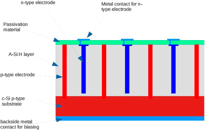
FIGURE 4. Lateral layout of a 3D a-Si:H p-i-n detector.
While the n-doped electrode is designed to be columnar, the p-doped electrode is foreseen in two possible shapes: columns and trenches. Figure 5 shows an upper view of one detector cell (1 n-type and 4 p-type contacts) in these two configurations.
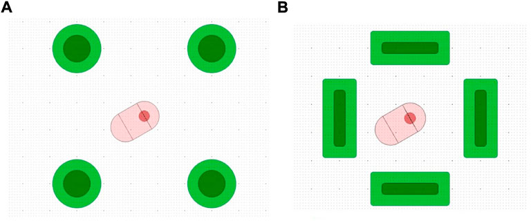
FIGURE 5. Top view of two cell types: (A) both n-doped (in red) and p-doped (in green) columnar electrode cell, and (B) n-type columnar and p-type trench electrode cell.
Aside from regular p or n doping achieved by ion implantation of boron and phosphor, another viable solution is possible—that is, the atomic layer deposition of charge selective low resistivity oxides: molybdenum oxide for hole selective contacts and titanium oxide or AZO (aluminum-doped zinc oxide ZnO:Al) for electron selective contacts. The devices fabricated with this technique have the same structure as the p-i-n devices, where p-doped layers are replaced by hole selective contact layers and n-doped layers are replaced with electron selective layer. This option has been validated with the fabrication and testing of planar prototype devices, which show good performance for x-ray monitoring—even better than similar p-i-n devices. A comparison between these two device architectures is reported in Ref. [28], where both p-i-n and charge selective contacts devices have been irradiated with neutrons.
Figure 6 shows the various phases of 3D a-Si:H detector fabrication:
a) Deposition of an intrinsic a-Si:H layer by PECVD;
b) Deposition and patterning of a mask for deep reactive ion etching (DRIE);
c) DRIE of holes and/or trenches;
d) Boron ion implantation or molybdenum oxide (for charge selective contact devices) atomic layer deposition (ALD) after deposition and patterning of a mask for implantation or ALD;
e) Phosphor ions implantation, or titanium oxide or AZO (for charge selective contact devices) ALD after deposition and patterning mask for implantation or ALD;
f) Etching and deposition, plus etching of passivating material before metallization;
g) Front side and backside metallization.
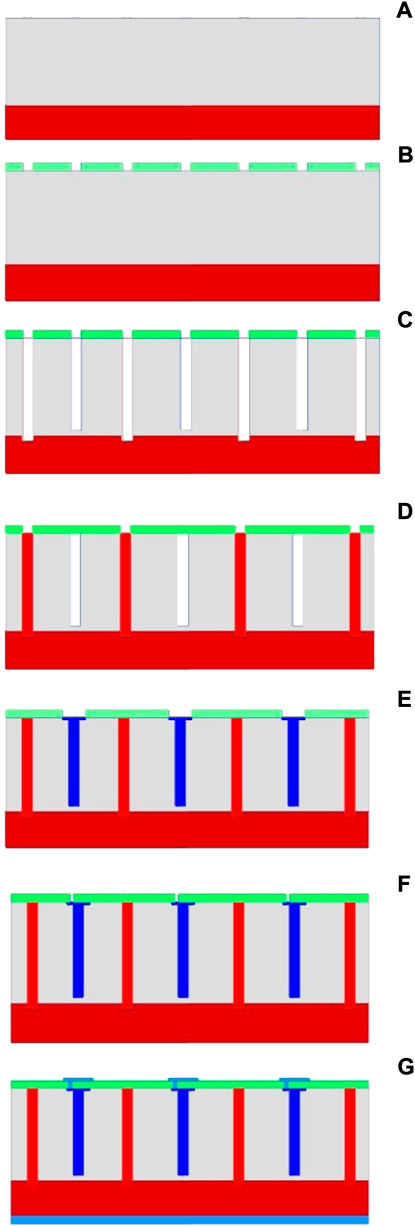
FIGURE 6. Various phases of a 3D a-Si:H detector fabrication (for a description of the various processing steps, see the list on section: 3D a-Si:H particle detectors).
Presently, 3D detectors are under development. Meanwhile, mechanical prototypes of columnar and trench type structures are under fabrication. When complete devices have been fabricated, these detectors will be bump bonded with the RD53A readout chip developed in the framework of the CMS and ATLAS experiments [29], and then tested in proton, x-ray, and electron beams.
The development of various types of ion beams—for example, reaccelerated ion beams, such as the INFN SPES project [30, 31], and clinical beams for radiotherapy, such as small beams [32, 33] or FLASH therapy [34]—drives the research for innovative ionizing radiation beam monitoring detectors. Most needed are transmission devices that are radiation resistant, have real-time response, do not saturate with high dose rate (high energy-per-pulse), and could provide a beam spatial profile.
The general requirements for these detectors are:
→ Thin sensitive layer with enough sensitivity per mm3 of material;
→ Small area devices (mm2 or less);
→ Small amount of material in the beam line to avoid disturbance of the delivered beam;
→ Resistance to radiation damage of the sensitive layer.
Meanwhile, a-Si:H detectors have already been used in proton beam monitoring applications at the CNAO accelerator hadrontherapy facility. A large (6 cm2 in area) a-Si:H planar detector was used to measure beam intensity with excellent linearity [24]. A proposal has recently been approved and funded to fabricate a sparse matrix of single sensing elements deposited on a thin plastic substrate, such as kapton or mylar. This detector matrix should be ultimately used at the end of a beam line in the flange that separates air from vacuum, providing at the same time a measurement of beam profile and beam flux.
The proof of concept for the capability of a-Si:H devices to be used to detect ionizing radiation has been demonstrated for a single charge selective contact diode with a sensitive layer that is 8.2 μm thick (Figure 7) that is exposed to an x-ray photon beam and to photon or electron clinical beams.
FIGURE 7. Picture of a-Si:H charge selective contact device prototype (4 × 4 × 0.0082 mm3 volume) deposited over glass substrate, composed of four identical devices.
The linearity of the measured current with respect to dose rate has been confirmed up to about 1% [25] with a sensitivity ranging from 1 to 20 nC/cGy. The possibility to use the device at 0 V bias has been also demonstrated with a noise of the order of 20 pA, assuring for a S/N value of 5 a detection threshold of 1 mGy/s. With 30 V bias, the charge collection efficiency increases more than one order of magnitude and the detection threshold lowers to 0.05 mGy/s.
To further increase the suitability of a-Si:H as detection material, the following aspects should be explored:
• The choice of the contact type: up to now charge selective contacts and p-i-n diodes have been employed, resulting in sensitivity differing by more than one order of magnitude;
• The H concentration in the sensor volume;
• The geometrical dimensions (area, thickness);
• The background current and its fluctuations as a function of temperature, bias, and sensor volume;
• Alternative types of deposition processes, such as PLD or sputtering in a hydrogen atmosphere.
Another promising application of a-Si:H for particle detection is amorphous silicon-based microchannel plates (AMCPs) [35]. Compared to a conventional lead glass microchannel plate, AMCPs offer two key benefits. First, the bulk conductivity of a-Si:H provides a charge replenishment after the emission of secondary electron without the need to coat the channel walls. With a more efficient replenishment, AMCPs are expected to exhibit shorter dead time (given by the charge replenishment time and large gain under continuous operation). Second, the fact that AMCPs are fabricated out of deposited layers allows for a monolithic integration on the readout electronics in the same fashion as TFA devices. This integration should provide low noise and low power consumption.
AMCP can be used alone for the detection of electrons, photons or other low energy particles that can interact with the channel walls to create secondary electron emission and initiate the avalanche. Alternatively, they can be coupled to a photocathode to create the primary photoelectron and may be eventually combined with a scintillator or radiator for high energy particle or MIP detection [36].
AMCPs have to be fabricated on a substrate (e.g., a silicon wafer or a readout chip) because they are fabricated from a stack of deposited layers (deposited by PECVD at temperatures <200°C), followed by micromachining of channels by deep reactive ion etching (DRIE). From that reason, AMCP cannot be stacked as standard microchannel plates (MCP) to multiply the gain and the channel cannot be slanted to increase the number of collisions (and as a consequence limiting the gain). However, state-of-the-art AMCPs exhibit gains similar to those of MCP with analog aspect ratio of the channels [35,36,37]. A typical structure of AMCPs is given in Figure 8.
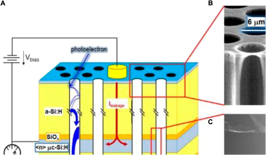
FIGURE 8. Schematic view of the AMCP architecture (A). A bias voltage of up to 600 V is applied between the top electrode and the intermediate one. The AMCP signal is recorded on the anode (bottom electrode). A thin a-Si:H layer is used to decouple (isolate) the anode from the intermediate electrode. Cross-sectional SEM images of the top of an AMCP, showing the current channel geometries, and the bottom layers are shown in (B,C). Image taken from [35].
The description of the AMCP operation and gain follows the same Eberhart model used for MCPs [38, 39]. Increasing the gain is therefore primarily dependent on the aspect ratio of the channel that can be achieved [40]. By optimizing the DRIE process, the aspect ratio has been increased from ca. 12.5 (as in [35]) to 25 in the latest generation of these devices. Such an increase has enabled us to multiply the gain by a factor of 30 to gain values of ca. 1,500 (Figure 9) [36].
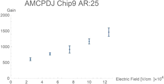
FIGURE 9. Measured gain value as a function of bias field in the channel for an AMCP with aspect ratio of 25. Image taken from [36].
To further increase the gain by a factor 2–3, the channel can be coated with a high secondary electron emissive layer, such as Al2O3 [35] or MgO [41]. In addition, the energy of the first incoming electron should be tuned to match the maximum of the secondary electron emission yield, providing up to another factor of 2 in the gain. Finally, with a further optimization of the DRIE process, an aspect ratio of up to 35 will add another boost. By combining these potential improvements, AMCP with gain values above 10′000 could be fabricated. These values exceed the best single plate conventional MCP.
While a-Si:H materials have attracted a lot of attention for particle detection since the 1980’s given their high radiation hardness, they have found very limited applications in high energy physics. The insufficient S/N ratios achieved so far for single particle detection is the main reason for their lack of success. An innovative 3D detector geometry and the implementation of selective contacts should help to considerably improve both the charge generation and the charge collection upon MIP interaction. The 3D detectors that are currently being fabricated have the potential to break the current bottleneck and to achieve a sufficient S/N ratio for MIP detection, while offering improved radiation resistance compared to state-of-the-art Si detectors.
Several clinical applications require radiation hard detectors that are able to provide real-time response without saturation at high dose rate. According to preliminary studies, a-Si:H detectors have the potential to fulfill these requirements. Furthermore, taking advantage of the possibility to deposit a-Si:H diodes on various substrates, the fabrication of flexible detectors on Kapton substrates is an attractive option. Detectors deposited on a thin substrate would also be very advantageous for beam profiling.
The use of a-Si:H as a bulk material for microchannel plates is actively studied. It offers several key advantages with respect to conventional devices, such as shorter charge replenishment time, lower probability of saturation, and the possibility of vertical integration on the readout electronics (monolithic integration). These devices are expected to achieve single photon detection with time resolution better than 20 ps. Several applications in medicine or in physics could benefit from such a development.
With these new developments, a-Si:H should finally find opportunities as active material for particle detection and allow for the fabrication of very radiation hard detectors.
MM wrote the introduction and the section on 3D a-Si:H detectors, LS: wrote the section on flexible a-Si:H detectors, and NW wrote the section about a-Si:H MCP and the conclusion.
The authors declare that the research was conducted in the absence of any commercial or financial relationships that could be construed as a potential conflict of interest.
All claims expressed in this article are solely those of the authors and do not necessarily represent those of their affiliated organizations, or those of the publisher, the editors and the reviewers. Any product that may be evaluated in this article, or claim that may be made by its manufacturer, is not guaranteed or endorsed by the publisher.
1. Chittick RC, Alexander JH, Sterling HF. The preparation and properties of amorphous silicon. J Electrochem Soc (1969) 116:77. doi:10.1149/1.2411779
2. Spear W, Lecomber PG. Electronic properties of substitutionally doped amorphous Si and Ge. Phil Mag (1976) 33:935–49. doi:10.1080/14786437608221926
3. Davis JA, Boscardin M, Crivellari M, Fano L, Large M, Menichelli M, et al. Modeling a thick hydrogenated amorphous silicon substrate for ionizing radiation detectors. Front Phys (2020) 8:158. doi:10.3389/fphy.2020.00158
4. Rech B, Wagner H. Potential of amorphous silicon for solar cells. Appl Phys A: Mater Sci Process (1999) 69:155–67. doi:10.1007/s003390050986
5. Menichelli M, Bizzarri M, Boscardin M, Caprai M, Caricato AP, Cirrone GAP, et al. Fabrication of a hydrogenated amorphous silicon detector in 3-D geometry and preliminary test on planar prototypes. Instruments (2021) 5:32. doi:10.3390/instruments5040032
6. Rech B, Wieder S, Siebke F, Beneking C, Wagner H. Material basis of highly stable a-Si:H solar cells. Mater Res Soc Symp Proc (1996) 420:33. doi:10.1557/proc-420-33
7. Shah S, Dutta J, Wyrsch N, Prasad K, Curtins H, Finger F, et al. VHF plasma deposition: A comparative overview. MRS Proc (1992) 258:15–26. doi:10.1557/proc-258-15
8. Paquin L, Masson D, Wertheimer MR, Moisan M. Amorphous silicon for photovoltaics produced by new microwave plasma-deposition techniques. Can J Phys (1985) 63:831–7. doi:10.1139/p85-134
9. Mahan A. Hot wire chemical vapor deposition of Si containing materials for solar cells. Sol Energ Mater Sol Cell (2003) 718:299–327. doi:10.1016/s0927-0248(02)00440-3
10. Wyrsch N, Ballif C. Review of amorphous silicon based particle detectors: The quest for single particle detection. Semicond Sci Technol (2016) 31:103005. doi:10.1088/0268-1242/31/10/103005
11. Srour JR, Vendura G, Lo D, Toporow C, Dooley M, Nakano R, et al. Damage mechanisms in radiation-tolerant amorphous silicon solar cells. IEEE Trans Nucl Sci (1998) 45:2624–31. doi:10.1109/23.736506
12. Boudry JM, Antonuk LE. Radiation damage of amorphous silicon photodiode sensors. IEEE Trans Nucl Sci (1994) 41:703–7. doi:10.1109/23.322792
13. Wyrsch N, Miazza C, Dunand S, Ballif C, Shah A, Despeisse M, et al. Radiation hardness of amorphous silicon particle sensors. J Non Cryst Sol (2006) 352:1797–800. doi:10.1016/j.jnoncrysol.2005.10.035
14. Diehl F, Herbst W, Bauer S, Schroder B, Oechsner H. Creation of metastable defects in a-Si:H by keV-electron irradiation at different temperatures. J Non Cryst Sol (1996) 198-200:436–40. doi:10.1016/0022-3093(95)00717-2
15. Perez-Mendez V, Cho G, Fujieda I, Kaplan S, Qureshi S, Street RA, et al. (1989). “The application of thick hydrogenated amorphous silicon layers to charge particle and x-ray detection,” Mater. Res. Soc. Proc., 149. 621–30.
16. Foulon F, Bergonzo P, Brambilla A, Jany C, Guizard B, Marshall RD. Neutron detectors made from chemically vapour deposited semiconductors. MRS Proc (1998) 487:591. doi:10.1557/proc-487-591
17. Mireshghi A, Cho G, Drewery J, Hong W, Jing T, Lee H, et al. High efficiency neutron sensitive amorphous silicon pixel detectors. IEEE Trans Nucl Sci (1994) 41:915–21. doi:10.1109/23.322831
18. Equer B, Karar A. Effect of primary ionization in amorphous silicon detectors. Nucl Instr Methods Phys Res Section A: Acc Spectrometers Detectors Associated Equipment (1988) 271:574–84. doi:10.1016/0168-9002(88)90324-5
19. Bacci C, Evangelisti F, Fiorini P, Furetta C, Meddi F, Mittiga A, et al. Detection of strongly ionizing particles with a hydrogenated amorphous silicon detector. Nucl Instr Methods Phys Res Section A: Acc Spectrometers Detectors Associated Equipment (1991) 306:182–6. doi:10.1016/0168-9002(91)90317-j
20. Schneider B. Image sensors in TFA (thin film on ASIC) technology handbook on computer vision an applications. Boston: Academic (1999). p. 237–70.
21. Miazza C C, Wyrsch N, Choong G, Dunand S, Ballif C, Shah A, et al. Image sensors based on thin-film on CMOS technology: Additional leakage currents due to vertical integration of the a-Si:H diodes. Mater Res Soc.Proc Symp (2006) 910:A17–03. doi:10.1557/PROC-0910-A17-03
22. Despeisse M, Anelli G, Jarron P, Kaplon J, Moraes D, Nardulli A, et al. Hydrogenated amorphous silicon sensor deposited on integrated circuit for radiation detection. IEEE Trans Nucl Sci (2008) 55:802–11. doi:10.1109/tns.2008.918519
23. Wyrsch N, Choong G, Miazza C, Ballif C. Performance and transient behavior of vertically integrated thin-film silicon sensors. Sensors (2008) 8:4656–68. doi:10.3390/s8084656
24. Caracciolo H, Balbinot G, Bazzano J, Bosser M, Caldara A, Pullia C, et al. Beam diagnostics commissioning at CNAO. Proc. of the 2nd Int. Particle Accelerator Conf; Sep, 2011; San Sebastain, Spain (2011). p. 2848–50.
25. Menichelli M, Bizzarri M, Boscardin M, Caprai M, Caricato A, Cirrone G, et al. Testing of planar hydrogenated amorphous silicon sensors with charge selective contacts for the construction of 3D-detectors. J Instrum (2020) 15:C03033. doi:10.1088/1748-0221/17/03/c03033
26. Menichelli M, Boscardin M, Crivellari M, Davis J, Dunand S, Fano L, et al. Hydrogenated amorphous silicon detectors for particle detection, beam flux monitoring and dosimetry in high-dose radiation environment. J Instrum (2022) 17:C04005. doi:10.1088/1748-0221/15/04/c04005
27. Menichelli M, Boscardin M, Crivellari M, Davis J, Dunand S, Fano L, et al. 3D Detectors on Hydrogenated Amorphous Silicon for particle tracking in high radiation environment. J Phys Conf Ser (2020) 1561:012016. doi:10.1088/1742-6596/1561/1/012016
28. Menichelli M, Bizzarri M, Boscardin M, Caprai M, Cupparo I, Wyrsch N, et al. Displacement damage in Hydrogenated Amorphous Silicon p-i-n diodes and charge selective contacts detectors. In: Presented at IEEE-NSS 2021(virtual) N31-05.Submitted to IEEE Trans. Nucl. Sci.; 2021 Oct 16-23, 2021; Yokohama, Japan. Preprint Available at: https://www.techrxiv.org/articles/preprint/Displacement_damage_in_Hydrogenated_Amorphous_Silicon_p-i-n_diodes_and_charge_selective_contacts_detectors_/19555042.
29. Gaioni L. Test results and prospects for RD53A, a large scale 65 nm CMOS chip for pixel readout at the HL-LHC. Nucl Instr Methods Phys Res Section A: Acc Spectrometers Detectors Associated Equipment (2019) A936:282–5. doi:10.1016/j.nima.2018.11.107
30. Andrighetto A, Biasetto L, Manzolaro M, Benetti P, Carturan S, Colombo P, et al. The SPES project at LNL. AIP Conf Proc (2009) 1099:728–32. doi:10.1063/1.3120141
31. Monetti A, Andrighetto A, Petrovich C, Manzolaro M, Corradetti S, Scarpa D, et al. The RIB production target for the SPES project. Eur Phys J A (2015) 51:128. doi:10.1140/epja/i2015-15128-6
32. Parwaie W, Refahi S, Ardekani MA, Farhood B. Different dosimeters/detectors used in small-field dosimetry: Pros and cons. J Med Signals Sens (2018) 8:195. doi:10.4103/jmss.JMSS_3_18
33. Bagheri H, Soleimani A, Gharehaghaji N, Mesbahi A, Manouchehri F, et al. An overview on small-field dosimetry in photon beam radiotherapy: Developments and challenges. J Cancer Res Ther (2017) 13:175. doi:10.4103/0973-1482.199444
34. Jolly S, Hywel O, Schippers M, Welsch C. Technical challenges for FLASH proton therapy. Physica Med (2020) 78:71–82. doi:10.1016/j.ejmp.2020.08.005
35. Franco A, Geissbühler J, Wyrsch N, Ballif C. Fabrication and characterization of monolithically integrated microchannel plates based on amorphous silicon. Sci Rep (2014) 4:4597. doi:10.1038/srep04597
36. Frey S, Ballif C, Wyrsch N. 2022 Amorphous silicon based microchannel plates for time-of-flight positron emission tomography. EPFL thesis Unpublished.
37. Loeffler J, Ballif C, Wyrsch N. Amorphous silicon-based microchannel plate detectors with high multiplication gain. Nucl Instr Methods Phys Res Section A: Acc Spectrometers Detectors Associated Equipment (2018) 912:343–6. doi:10.1016/j.nima.2017.12.036
38. Eberhardt EH. Gain model for microchannel plates. Appl Opt (1979) 18(9):1418–23. doi:10.1364/ao.18.001418
39. Eberhardt EH. An operational model for microchannel plate devices. IEEE Trans Nucl Sci (1981) 28(1):712–7. doi:10.1109/tns.1981.4331267
40. Frey S, Löffler J, Ballif C, Wyrsch N. Characterization of amorphous silicon based microchannel plates with high aspect ratio. In: IEEE Nuclear Science Symposium and Medical Imaging Conference (NSS/MIC); 26 Oct-2 Nov, 2019. Manchester, UK (2019). doi:10.1109/NSS/MIC42101.2019.9059714
Keywords: tracking detector, radiation hard detector, hydrogenate amorphous silicon (a-Si:H), beam flux monitoring, microchannel plate (MCP) detectors, flexible detector
Citation: Menichelli M, Servoli L and Wyrsch N (2022) Status and perspectives of hydrogenated amorphous silicon detectors for MIP detection and beam flux measurements. Front. Phys. 10:943306. doi: 10.3389/fphy.2022.943306
Received: 13 May 2022; Accepted: 09 September 2022;
Published: 04 October 2022.
Edited by:
Gian-Franco Dalla Betta, University of Trento, ItalyReviewed by:
Bjarne Stugu, University of Bergen, NorwayCopyright © 2022 Menichelli, Servoli and Wyrsch. This is an open-access article distributed under the terms of the Creative Commons Attribution License (CC BY). The use, distribution or reproduction in other forums is permitted, provided the original author(s) and the copyright owner(s) are credited and that the original publication in this journal is cited, in accordance with accepted academic practice. No use, distribution or reproduction is permitted which does not comply with these terms.
*Correspondence: M. Menichelli, bWF1cm8ubWVuaWNoZWxsaUBwZy5pbmZuLml0
Disclaimer: All claims expressed in this article are solely those of the authors and do not necessarily represent those of their affiliated organizations, or those of the publisher, the editors and the reviewers. Any product that may be evaluated in this article or claim that may be made by its manufacturer is not guaranteed or endorsed by the publisher.
Research integrity at Frontiers
Learn more about the work of our research integrity team to safeguard the quality of each article we publish.