 Yanshuo Feng1
 Misheng Liang
94% of researchers rate our articles as excellent or good
Learn more about the work of our research integrity team to safeguard the quality of each article we publish.
Find out more
MINI REVIEW article
Front. Phys., 04 July 2022
Sec. Optics and Photonics
Volume 10 - 2022 | https://doi.org/10.3389/fphy.2022.918372
This article is part of the Research TopicAdvances in Laser Micro-Processing and ApplicationsView all 5 articles
Noble metal plasmonic nanostructures have a wide range of applications in surface-enhanced Raman scattering (SERS), solar energy conversion, optical imaging, biosensing, and many other fields due to their unique localized surface plasmon resonance effects and optical properties. In recent years, the fabrication method of noble metal plasmonic nanostructures has attracted a lot of research interest. Compared with traditional processing methods, femtosecond laser processing has the advantages of high processing resolution, small heat-affected zone, high processing flexibility, controllability, and ease of patterning, and has shown great potential for application in the fabrication method of noble metal plasmonic nanostructures. In this paper, the recent advances in the fabrication of noble metal plasmonic nanostructures by femtosecond laser are reviewed, followed by a discussion of the characteristics, advantages, and potential applications of the structures prepared by this method.
Plasmonic nanostructures of noble metals (gold, silver etc.,) have localized surface plasmon resonance (LSPR) [1]. Noble metal plasmonic nanostructures are characterized by their stronginteractions with photons through an excitation of LSPR. When the photons are matched with the oscillation frequencies of the metal conduction electrons, resonance effects with surface electromagnetic local enhancement and near-field enhancement [2] are produced. Because of this unique property of plasmonic nanostructures, it has played an important role in biosensing [3, 4], medical imaging [5, 6], food quality inspection [7], environmental analysis [8], energy conversion [9, 10], surface-enhanced Raman scattering (SERS) signal detection [11, 12] and other fields.
In the last decades, fabrication methods of noble metal plasmonic nanostructures have attracted a great deal of interest. At present, fabrication technologies of noble metal plasmonic nanostructures have been developed, such as electron beam lithography (EBL) [13], focused ion beam (FIB) [14], nanoimprint technology [15, 16], self-assembly technology [17], 3D printing technology [18, 53], etc., Although the above processing methods have achieved the fabrication of noble metal plasmonic nanostructures, several drawbacks of the above mentioned methods still need to overcome, such as cumbersome processing technology and poor controllability.
In recent years, with the rapid development of laser processing technology, femtosecond laser processing technology has demonstrated unique advantages in micro/nano fabrication. Femtosecond laser processing technology has an ultra-short pulse width (10–15 s) and a strong instantaneous peak power (1014 W/cm2) [19], which makes its interaction with the material exhibit strong non-linear and non-equilibrium characteristics [20–22]. Compared to conventional long pulse lasers or continuous lasers, femtosecond laser micromachining technology has the following advantages:
(1) High Processing Resolution
Ultrafast laser processing has a strong threshold effect, where the material can only be removed when the laser fluence (or power density) exceeds the material ablation threshold. Therefore, when the pulsed laser energy is reduced, only a smaller fraction of the focused spot energy exceeds the ablation threshold, contributing to the formation of subdiffraction-limited structures. In addition, the ultrafast laser-material interaction process has a significant nonlinear effect, when the photon energy is smaller than the material forbidden band width, the optical absorption is dominated by two-photon or multi-photon ionization and other nonlinear absorption processes, and the processing results can easily break the optical diffraction limit. Based on this principle, ultrafast laser two-photon polymerization methods typified by “nanobowls” [23] and 3D printing technologies represented by “minimal human sculptures” have been widely studied with processing accuracy and resolution much smaller than the diffraction limit.
(2) Small Heat-affected Zone
The material electron-lattice heat transfer time is in the nanosecond to picosecond order (10−10−10−12 s) [20]. During nanosecond (10−9 s) laser processing, the energy transfer process of the excited electrons is completed within the pulse duration, allowing the electrons and lattice to remain in equilibrium at all times [24–26]. During femtosecond laser processing, the absorption of femtosecond photon energy by the material is initially accomplished primarily by the electrons as carriers because the femtosecond laser pulse width is much smaller than the electron-lattice thermal conduction time. During the femtosecond pulse irradiation time, the material lattice motion can be neglected and the electron-lattice is in a non-equilibrium state. Although the irradiation time of the femtosecond laser pulse is very short (on the order of femtoseconds), all subsequent processes (on the order of ∼seconds) are determined by the interaction of the femtosecond laser with the electrons. Therefore, femtosecond laser processing has the advantages of high quality and reproducibility [27].
(3) Almostly any material can be processed
The instantaneous peak power of a focused femtosecond laser pulse easily exceeds 1014 (W/cm2) [28] and can ionize and process virtually any material, including dielectrics, semiconductors, and metals. Compared to conventional processing methods, femtosecond lasers offer significant advantages in processing transparent hard and brittle materials such as fused silica, highly viscous materials such as organic/inorganic polymers, and ultra-hard materials such as diamond and silicon carbide.
Due to the aforementioned advantages, femtosecond laser micro and nano processing technology gradually become one of the most important methods for preparing plasma nanostructures of precious metals. In recent years, a variety of methods for femtosecond laser processing of plasmonic nanostructures have been developed. This paper reviews the femtosecond laser fabrication method of noble metal nanostructures and its applications, and will further investigate the femtosecond laser processing of multi-metal plasma nanostructures in the future.
The femtosecond laser fabrication methods for noble metal plasmonic structures are generally divided into two categories. The first is based on the “top-down” principle, where the material is removed through femtosecond laser fabrication to obtain the nanostructures with specific shapes and sizes. The second category is based on the “bottom-up” principle, based on the chemical properties of self-assembly to grow new structures on top of the original structure to form a basic surface micro-nano-arranged structure, the main methods include multi-photon polymerization [29, 30], metal salt solution reduction [31, 32], metal particle sintering [33, 34], and laser-induced forward transfer [35].
(1) Top-down
The top-down processing method mainly obtains noble metal nanostructures with resonance effect through the removal of materials by femtosecond laser ablation. This kind of method has the advantage of simplicity, flexibility, and easy pattern. However, due to the optical diffraction limit, the ablative structuring of nanoscale structures is difficult in most cases. Therefore, the biggest challenge of this type of method is how to overcome the optical diffraction limit to ablate and remove materials.
Femtosecond lasers have strong nonlinear processes during their interaction with materials, such as two-photon/multi-photon absorption, and multi-photon ionization processes. The nonlinear effects generated by femtosecond lasers can be used to capture or manipulate particles, thus enabling high-precision controlled fabrication of nanostructures [37]. For example, Liu’s group used femtosecond laser direct processing of metal-transparent metal oxides. The fabrication mechanism is attributed to light-induced melt oxidation, which uses non-linear effects to limit the size of the oxidized region, enabling sub-wavelength processing [38, 39] (Figure 1A). In 2020, Huang et al.used femtosecond laser to process the 3D shell-like structures of gold films. Under the action of non-linearity, gold nanoparticles can be stably trapped at a special position. With the help of lens observation, a double trap with a separation distance of less than 100 nm was achieved [40] (Figure 1B, Figure 1C) .
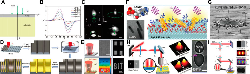
FIGURE 1. Femtosecond laser top-down preparation method figure (A) Schematic view of the fabrication of the MTMO grayscale photomasks [39] (B) femtosecond laser capture of Au nanoparticles [40] (C) experimental results of gold nanoparticles trapped by femtosecond laser [40] (D) AuNPDN substrate manufacturing process diagram [42] (E) Schematic diagram of Au3+ reduction in two steps [43] (F) schematic diagram of laser induced gold nanorod plasma nanostructure [44] (G) side view of a nanopin made by optical vortex [45] (H) space shaping experimental setup and pulse ablation of metal films [46] (I) spatial shaping experimental setup and step-by-step experimental procedures [47].
Femtosecond Laser-Induced Periodic Surface Structures (LIPSS) provides a simple approach to maintain noble metal plasmonic nanostructures. The LIPSS structure has a subwavelength periodic grating structure [41]. The structure can be formed by laser irradiation on almost any material surface and has the advantages of being simple and controllable, easy to prepare in large areas, and has been widely used. Since LIPSS has nanoscale array structure characteristics, it can provide a structural basis for the formation of noble metal plasma nanostructures. For example, Cao et al. proposed a new method to fabricate Au nanoparticle-decorated nanorod (NPDN) arrays by femtosecond laser. The nanogap and diameter of the prepared Au nanoparticles significantly affect the performance of SERS, while the enhancement factor of the substrate decorated with gold nanoparticles can be controlled up to 8.3 × 10⁷ [42] (Figure 1D). In 2019, Li et al. proposed a method to obtain local electric field enhancement using femtosecond laser-induced periodic surface structures, which enables the deposition of gold nanoparticles on silicon substrates with excellent spatial selectivity and uniformity. This method provides a new strategy for preparing gold plasma nanoparticles on SERS substrates, which has great potential for applications in molecular detection and biosensing [43] (Figure 1E). In addition, in 2020, Yeshchenko et al. used femtosecond laser-induced silver periodic surface structures and gold nanorods or nanospheres to form plasmonic nanocavities. This structure is expected to be used for high-sensitivity label-free detection and imaging of biomolecules under the greenhouse [44] (Figure 1F).
Spatial modulating of laser pulses can break the diffraction limit and enable the processing of smaller size structures. For example, Toyoda et al. used a spatially shaped vortex-beam laser to generate plasmonic nanostructures on metal surfaces with chiral needles whose tip curvature was measured to be less than 40 nm (less than 1/25 of the laser wavelength) [45] (Figure 1G). The structures provide a favorable method for selectively distinguishing nanoscale molecules from chemical composites. Wang et al. used the femtosecond laser spatial shaping to process gold nanowires with a minimum width of 56 nm (only 1/14 of the wavelength of the incident laser) and a conductivity of 25% of that of the bulk material [46] (Figure 1H). In 2019, Xu et al. used spatially shaped femtosecond laser pulses to fabricate gold bowtie nanostructures. By adjusting the pulse energy to control the size of the nanostructures, this method produced a minimum nanogap of 30 nm (the more 1/26 of the laser wavelength), which allows the patterning of large-area micro-nano structures on terahertz supersurfaces [47] (Figure 1I).
(2) Bottom-up
The bottom-up processing enables the additive forming of nanostructures by means of the reductionism, the deposition or the polymerization of atoms, molecules or other nanoparticles controlled by a femtosecond laser. Based on the characteristics of additive manufacturing, such methods have unique advantages in the processing of 3D nanostructures.
Femtosecond laser direct writing processing is the most fundamental processing method from the bottom-up, using a femtosecond laser to “write” directly on the material. For example, in 2017, Han et al. showed that the resonance scattering spectra of gold nanobulge structures exhibited two resonance peaks by femtosecond laser-induced dewetting effect for the fabricate of gold nanobulge structures. This method became an effective means of extending the fabrication of patterned functional nanostructures [48] (Figure 2A). In 2018, Jradi et al. proposed the site-selective dewetting of metal thin films by a femtosecond laser direct writing system to prepare gold nanoparticles. The method is suitable for the inheritance of ultra-high sensitivity plasma microchips for the detection of analyte fingerprints for SERS [49] (Figure 2B).
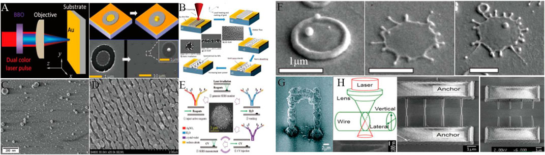
FIGURE 2. Femtosecond laser bottom-up preparation method (A) femtosecond laser direct-write processing experimental setup and single nanoparticles formed by irradiation on an early semiconductor substrate [48] (B) mechanisms of nanoparticle preparation on gold films by femtosecond laser direct writing processing [49] (C) SEM image of the deposited material after laser pulse irradiation [34] (D) laser deposition of gold nanoparticles [35] (E) nanostructures formed by femtosecond laser-induced metal reduction [32] (F) aggregate photo-induced growth of silver nanoparticles prepared by sputtering deposition [36] (G) three-dimensional structures formed by two-photon polymerization preparation [30] (H) hanging wire array diagram [31].
Femtosecond laser sintering describes the physical change of the material surface by the nonlinear absorption of the pulse energy of various materials under the action of the strong field generated by the femtosecond laser. As a result, various complex shapes are formed on the surface or inside the material. For example, in 2017, Nedyalkov et al. demonstrated the use of femtosecond lasers to ablate gold targets in air and deposit material structures, with the deposition process leading to the formation of plasmonic nanostructures on substrate substrates. The method demonstrated that the presented nanostructures can be accomplished in an open-air environment for direct deposition, which has important applications in sensor fabrication, catalysis, and other fields [34] (Figure 2C). Furthermore, in 2020, Donnelly et al. used femtosecond laser ablation in argon to deposit gold nanoparticles, controlling the equivalent thickness of the nanoparticle films in the range of 0.4–28 nm by varying the target-substrate spacing and the firing spacing of the ablation point grating. It is experimentally demonstrated that all films show surface plasmon resonance at ∼525 nm out. This technique can be easily used to fabricate nanoparticle films at atmospheric pressure [35] (Figure 2D).
Femtosecond laser irradiation of metal precursor solutions (such as chloroauric acid or silver nitrate) can directly reduce metal cations to neutral atoms and form various noble metal plasma nanostructure [50]. This method is green, does not require any chemical reducing agent or surface capping agent, and has in situ reduction capability. For example, in 2017, P. Barton et al. employed a femtosecond laser (800 nm center wavelength, 23 fs pulse width) to induce silver nanoreduction in solution to generate silver nanostructures and evaluated the effect of solution chemistry on the prepared structures. The method can be used for direct laser fabrication of plasmonic metal nanostructures for plasmonics and microelectronics applications in nanoelectronics, and applications in acoustic wave and micro-nano electronics [32] (Figure 2E). In the same year, Li et al. prepared silver nanosheet arrays using focused femtosecond laser-induced photoreduction of metal salt solutions, and the fabrication of this structure would serve as silver nanoparticle aggregates for SERS monitor [33].
Laser induced forward transfer (LIFT) [51] can be performed by laser irradiation of the donor to cause melting or phase change of the sacrificial substrate. This results in the transfer of the desired structure to the recipient substrate. In this method the material is processed to produce higher precision and complex patterns without damaging the properties of the material. For example, Claas et al. used the laser-induced forward transfer method to control the deposition of copper and gold droplets to construct micro-pillars with a high depth to width ratio. They are less than 5 μm in diameter and up to 2 mm in length, and have low porosity and homogeneous electrical conductivity [36] (Figure 2F).
Two-photon polymerisation enables the fabrication of three-dimensional structures by direct solidification within the material through the non-linear two-photon absorption effect [52]. For example, in 2006, Takuo Tanaka et al. generated two-dimensional and “self-standing” three-dimensional structures of metals with electrical conductivity by two-photon induced reduction of metal ions (silver or gold ions) with a resistance 3.3 times that of bulk materials. However, due to the agglomerative growth of the reduced metal particles, the quality of the resulting metal structures is poor, with micron scales and poor quality of the resulting 3D structures [30] (Figure 2G). Using a two-photon absorption mechanism, Sun’s group has achieved a silver-palladium composite pattern with a controlled composition ratio, which can potentially be used as a robust surface-enhanced Raman spectroscopy (SERS) substrate inside a microfluidic chip [31] (Figure 2H) (Table 1).
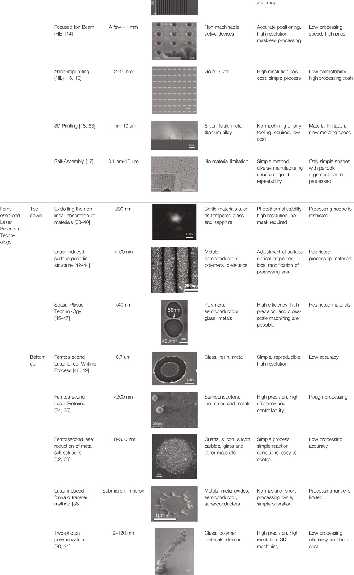
TABLE 1. Summary of preparation methods for plasma nanostructures of precious metals, including processing accuracy, advantages and disadvantages.
Metal plasmonic nanostructures have been fabricated on a large scale by femtosecond laser technology. They have shown unique applications value in different fields.
In the field of energy conversion, plasma nanostructures can facilitate the migration of photogenerated carriers through the LSPR effect, thus promoting the utilization of solar energy. For example, a recent study by Linic et al. showed that composite modules of noble metal plasma nanostructures as well as doped semiconductor structures of photocatalysts significantly enhanced water splitting to convert solar energy into chemical energy [10]. Paul et al. explored noble metal plasma nanostructures decorated with titanium dioxide to enhance the solar light-driven photocatalytic effect to convert light energy directly into electricity [9].
In the field of biosensing, localized surface plasmon resonance enables metal nanostructures to offer advantages of directional transmission, localized hot spots, enhanced resonance coupling and magnetic field, improving the sensitivity of biomolecule detection. For example, Rifat et al. proposed a new type of biosensor based on metal plasmon resonance in photonic crystal fibres, which detects unknown analytes by changes in the sensitivity of the metal surface. The sensitivity of the molecular detection was significantly improved [3]. Akjouj et al. optimized the structure of the sensor by depositing double-layer molybdenum disulfide/graphene layer on nanoparticles or adding a single-layer molybdenum disulfide layer/graphene layer on the surface of gold nanoparticles, which greatly improved the sensitivity of molecular detection [4].
In the field of SERS signal detection, SERS is used as a powerful vibrational spectroscopy technique that can accomplish highly sensitive detection of signal molecules by amplifying the electromagnetic field generated by localized surface plasma excitation. Huang et al. combined plasmonic nanostructures with a tapered fiber optic probes for surface-enhanced Raman scattering, which can be used for SERS-based liquid sample detection as well as SERS-based remote quality monitoring of liquid and biological substances [11]. Zhang et al. demonstrated the use of gold nanoparticle substrates for surface-enhanced Raman scattering using femtosecond pulses for grid scanning. The structure exhibits high surface activity and excellent substrate reproducibility and stability, allowing clear presentation of the Raman spectra of the target analytes [12].
In the field of optical imaging, plasma-coupled scanning near-field optical microscopy has emerged to overcome the optical diffraction limit. The interaction between metal nanoparticles is of great interest in optical imaging as a signal enhancement mechanism, and thus its correlation with optical properties needs to be fully exploited. For example, Pang et al. explored that gold nanostructures can be excited to emit relatively strong luminescence through their two-photon absorption mechanism. When certain conditions are reached, the excitation efficiency is significantly increased and optical imaging can be easily presented and used to quantify the cell detection [5]. Hou et al. reported that far-field imaging cannot capture the swift waves carrying nanoscale electric field information due to the near-field nature of the plasma on the inner surface of metal nanostructures. Therefore the correlation between gold nanostructures and optical properties was exploited to improve the resolution of imaging [6].
In recent years, femtosecond laser processing technology has emerged as a flexible, convenient and controllable method for the preparation of high-precision noble metal plasmonic nanostructures. In this paper, we compare femtosecond laser processing technology with traditional plasmonic nanostructure processing methods and summarize the advantages and disadvantages of each method. Firstly, we introduce the advantages of femtosecond laser processing technology as a new processing technology compared to traditional processing methods, and compare the femtosecond laser with traditional processing methods. Secondly, the current progress that has been made in the preparation of precious metal plasma nanostructures by femtosecond lasers is presented, focusing on the preparation of precious metal plasma nanostructures with femtosecond laser processing technology. The third part combines the experimental findings with theoretical models by understanding the relationship between the size, dimensions, and compositional morphology of noble metal plasmonic nanostructures and LSPR properties. The fourth part demonstrates the high application value of femtosecond laser preparation of noble metal plasmonic nanostructures, which can be used to a greater extent in real-life applications. Despite the impressive scientific achievements to date in the preparation of noble metal plasmonic nanostructures by femtosecond lasers, the continuous optimization of femtosecond lasers for efficient preparation of plasmonic nanostructures is still a novel field. In conclusion, femtosecond laser processing represents a new type of processing technology, which has been proven to be applied in various fields. In the future, it will continue to precisely control processing efficiency and processing materials and expand the scope of application.
In the list of authors, YF is the first author of the article; ML has summarized and critically suggested the work; RY and TL have provided valuable suggestions for the work; LZ is the corresponding author of this work.
The research was supported by the National Key Research and Development Program of China (Grant No. 2021YFB3201300), Beijing Nova Program (Grant No. Z211100002121075), Young Elite Scientist Sponsorship Program by CAST (Grant No. YESS20210023).
The authors declare that the research was conducted in the absence of any commercial or financial relationships that could be construed as a potential conflict of interest.
All claims expressed in this article are solely those of the authors and do not necessarily represent those of their affiliated organizations, or those of the publisher, the editors and the reviewers. Any product that may be evaluated in this article, or claim that may be made by its manufacturer, is not guaranteed or endorsed by the publisher.
1. Liu J, He H, Xiao D, Yin S, Ji W, Jiang S, et al. Recent Advances of Plasmonic Nanoparticles and Their Applications. Materials (2018) 11(10):1833. doi:10.3390/ma11101833
2. Su K-H, Wei Q-H, Zhang X, Mock JJ, Smith DR, Schultz S. Interparticle Coupling Effects on Plasmon Resonances of Nanogold Particles. Nano Lett (2003) 3(8):1087–90. doi:10.1021/nl034197f
3. Rifat AA, Mahdiraji GA, Sua YM, Ahmed R, Shee YG, Adikan FRM. Highly Sensitive Multi-Core Flat Fiber Surface Plasmon Resonance Refractive index Sensor. Opt Express (2016) 24(3):2485–95. doi:10.1364/oe.24.002485
4. Akjouj A, Mir A. Design of Silver Nanoparticles with Graphene Coatings Layers Used for LSPR Biosensor Applications. Vacuum (2020) 180:109497. doi:10.1016/j.vacuum.2020.109497
5. Pang B, Yang X, Xia Y. Putting Gold Nanocages to Work for Optical Imaging, Controlled Release and Cancer Theranostics. Nanomedicine (2016) 11(13):1715–28. doi:10.2217/nnm-2016-0109
6. Hou B, Xie M, He R, Ji M, Trummer S, Fink RH, et al. Microsphere Assisted Super-resolution Optical Imaging of Plasmonic Interaction between Gold Nanoparticles. Sci Rep (2017) 7(1):13789–10. doi:10.1038/s41598-017-14193-3
7. Zhou H, Li X, Wang L, Liang Y, Jialading A, Wang Z, et al. Application of SERS Quantitative Analysis Method in Food Safety Detection. Rev Anal Chem (2021) 40(1):173–86. doi:10.1515/revac-2021-0132
8. Li DW, Zhai WL, Li YT, Long YT. Recent Progress in Surface Enhanced Raman Spectroscopy for the Detection of Environmental Pollutants. Microchimica Acta (2014) 181(1):23–43. doi:10.1007/s00604-013-1115-3
9. Paul KK, Sreekanth N, Biroju RK, Narayanan TN, Giri PK. Solar Light Driven Photoelectrocatalytic Hydrogen Evolution and Dye Degradation by Metal-free Few-Layer MoS2 nanoflower/TiO2(B) Nanobelts Heterostructure. Solar Energ Mater Solar Cell (2018) 185:364–74. doi:10.1016/j.solmat.2018.05.056
10. Linic S, Christopher P, Ingram DB. Plasmonic-metal Nanostructures for Efficient Conversion of Solar to Chemical Energy. Nat Mater (2011) 10(12):911–21. doi:10.1038/nmat3151
11. Huang Z, Lei X, Liu Y, Wang Z, Wang X, Wang Z, et al. Tapered Optical Fiber Probe Assembled with Plasmonic Nanostructures for Surface-Enhanced Raman Scattering Application. ACS Appl Mater Inter (2015) 7(31):17247–54. doi:10.1021/acsami.5b04202
12. Zhang W, Li C, Gao K, Lu F, Liu M, Li X, et al. Surface-enhanced Raman Spectroscopy with Au-Nanoparticle Substrate Fabricated by Using Femtosecond Pulse. Nanotechnology (2018) 29(20):205301. doi:10.1088/1361-6528/aab294
13. Chang THP, Mankos M, Lee KY, Muray LP. Multiple Electron-Beam Lithography. Microelectronic Eng (2001) 57-58:117–35. doi:10.1016/s0167-9317(01)00528-7
14. Garg V, Mote RG, Fu J. Focused Ion Beam Direct Fabrication of Subwavelength Nanostructures on Silicon for Multicolor Generation. Adv Mater Technol (2018) 3(8):1800100. doi:10.1002/admt.201800100
15. Chou SY, Krauss PR, Renstrom PJ. Imprint of Sub‐25 Nm Vias and Trenches in Polymers. Appl Phys Lett (1995) 67(21):3114–6. doi:10.1063/1.114851
16. Chen W, Tymchenko M, Gopalan P, Ye X, Wu Y, Zhang M, et al. Large-area Nanoimprinted Colloidal Au Nanocrystal-Based Nanoantennas for Ultrathin Polarizing Plasmonic Metasurfaces. Nano Lett (2015) 15(8):5254–60. doi:10.1021/acs.nanolett.5b02647
17. Liu D, Li C, Zhou F, Zhang T, Liu G, Cai W, et al. Capillary Gradient-Induced Self-Assembly of Periodic Au Spherical Nanoparticle Arrays on an Ultralarge Scale via a Bisolvent System at Air/Water Interface. Adv Mater Inter (2017) 4(10):1600976. doi:10.1002/admi.201600976
18. Haring AP, Khan AU, Liu G, Johnson BN. 3D Printed Functionally Graded Plasmonic Constructs. Adv Opt Mater (2017) 5(18):1700367. doi:10.1002/adom.201700367
19. Liu X, Du D, Mourou G. Laser Ablation and Micromachining with Ultrashort Laser Pulses. IEEE J Quan Electron. (1997) 33(10):1706–16. doi:10.1109/3.631270
20. Costache F. Dynamics of Ultra-short Laser Pulse Interaction with Solids at the Origin of Nanoscale Surface Modification. BTU Cottbus-Senftenberg (2006).
21. Bulgakova NM. Fundamentals of Ultrafast Laser Processing. In: Ultrafast Laser Processing: From Micro-to Nanoscale (2013). p. 99–182.
22. Stafe M, Marcu A, Puscas NN Pulsed Laser Ablation of Solids: Basics, Theory and Applications, 53. Springer Science & Business Media (2013).
23. Wang H, Zhang Y-L, Wang W, Ding H, Sun H-B. On-chip Laser Processing for the Development of Multifunctional Microfluidic Chips. Laser Photon Rev (2017) 11(2):1600116. doi:10.1002/lpor.201600116
24. Zhang Y, Tzou DY, Chen JK. Micro-and Nanoscale Heat Transfer in Femtosecond Laser Processing of Metals[J]. arXiv preprint arXiv:1511.03566, 2015.
25. Zhang Y, Chen JK. An Interfacial Tracking Method for Ultrashort Pulse Laser Melting and Resolidification of a Thin Metal Film. J Heat Transfer (2008) 130(6):1159. doi:10.1115/1.2891159
26. Phillips KC, Gandhi HH, Mazur E, Sundaram SK. Ultrafast Laser Processing of Materials: a Review. Adv Opt Photon (2015) 7(4):684–712. doi:10.1364/aop.7.000684
27. Seel M, Domcke W. Femtosecond Time‐resolved Ionization Spectroscopy of Ultrafast Internal‐conversion Dynamics in Polyatomic Molecules: Theory and Computational Studies. J Chem Phys (1991) 95(11):7806–22. doi:10.1063/1.461816
28. Jiang L, Wang A-D, Li B, Cui T-H, Lu Y-F. Electrons Dynamics Control by Shaping Femtosecond Laser Pulses in Micro/nanofabrication: Modeling, Method, Measurement and Application. Light Sci Appl (2018) 7(2):17134. doi:10.1038/lsa.2017.134
29. Joshi CJ, Corkum PB. Interactions of Ultra‐Intense Laser Light with Matter. Phys Today (1995) 48(1):36–43. doi:10.1063/1.881451
30. Tanaka T, Ishikawa A, Kawata S. Two-photon-induced Reduction of Metal Ions for Fabricating Three-Dimensional Electrically Conductive Metallic Microstructure. Appl Phys Lett (2006) 88(8):081107. doi:10.1063/1.2177636
31. Ma Z-C, Zhang Y-L, Han B, Liu X-Q, Zhang H-Z, Chen Q-D, et al. Femtosecond Laser Direct Writing of Plasmonic Ag/Pd alloy Nanostructures Enables Flexible Integration of Robust SERS Substrates. Adv Mater Technol (2017) 2(6):1600270. doi:10.1002/admt.201600270
32. Barton P, Mukherjee S, Prabha J, Boudouris BW, Pan L, Xu X. Fabrication of Silver Nanostructures Using Femtosecond Laser-Induced Photoreduction. Nanotechnology (2017) 28(50):505302. doi:10.1088/1361-6528/aa977b
33. Yan W, Yang L, Chen J, Wu Y, Wang P, Li Z. In Situ Two-Step Photoreduced SERS Materials for On-Chip Single-Molecule Spectroscopy with High Reproducibility. Adv Mater (2017) 29(36):1702893. doi:10.1002/adma.201702893
34. Nedyalkov N, Nikov R, Dikovska A, Atanasova G, Nakajima Y, Terakawa M. Gold Nanostructures Deposition by Laser Ablation in Air Using Nano-And Femtosecond Laser Pulses. Appl Phys A (2017) 123(5):1–11. doi:10.1007/s00339-017-0878-5
35. Donnelly T, O’Connell G, Lunney JG. Metal Nanoparticle Film Deposition by Femtosecond Laser Ablation at Atmospheric Pressure. Nanomaterials (2020) 10(11):2118. doi:10.3390/nano10112118
36. Visser CW, Pohl R, Sun C, Römer G-W, Huis in ‘t Veld B, Lohse D. Toward 3D Printing of Pure Metals by Laser‐induced Forward Transfer. Adv Mater (2015) 27(27):4087–92. doi:10.1002/adma.201501058
37. Usman A, Chiang W-Y, Masuhara H. Optical Trapping of Nanoparticles by Ultrashort Laser Pulses. Sci Prog (2013) 96(1):1–18. doi:10.3184/003685013x13592844053451
38. Xia F, Zhang X, Wang M, Liu Q, Xu J. Analysis of the Laser Oxidation Kinetics Process of In-In_2O_3 MTMO Photomasks by Laser Direct Writing. Opt Express (2015) 23(22):29193–201. doi:10.1364/oe.23.029193
39. Xia F, Zhang X, Wang M, Yi S, Liu Q, Xu J. Numerical Analysis of the Sub-wavelength Fabrication of MTMO Grayscale Photomasks by Direct Laser Writing. Opt Express (2014) 22(14):16889–96. doi:10.1364/oe.22.016889
40. Huang L, Qin Y, Jin Y, Shi H, Guo H, Xiao L, et al. Spheroidal Trap Shell beyond Diffraction Limit Induced by Nonlinear Effects in Femtosecond Laser Trapping. Nanophotonics (2020) 9(14):4315–25. doi:10.1515/nanoph-2020-0288
41. Hwang JS, Park J-E, Kim GW, Lee H, Yang M. Fabrication of Printable Nanograting Using Solution-Based Laser-Induced Periodic Surface Structure Process. Appl Surf Sci (2021) 547:149178. doi:10.1016/j.apsusc.2021.149178
42. Cao W, Jiang L, Hu J, Wang A, Li X, Lu Y. Optical Field Enhancement in Au Nanoparticle-Decorated Nanorod Arrays Prepared by Femtosecond Laser and Their Tunable Surface-Enhanced Raman Scattering Applications. ACS Appl Mater Inter (2018) 10(1):1297–305. doi:10.1021/acsami.7b13241
43. Li C, Hu J, Jiang L, Xu C, Li X, Gao Y, et al. Shaped Femtosecond Laser Induced Photoreduction for Highly Controllable Au Nanoparticles Based on Localized Field Enhancement and Their SERS Applications. Nanophotonics (2020) 9(3):691–702. doi:10.1515/nanoph-2019-0460
44. Yeshchenko OA, Golovynskyi S, Kudrya VY, Tomchuk AV, Dmitruk IM, Berezovska NI, et al. Laser-induced Periodic Ag Surface Structure with Au Nanorods Plasmonic Nanocavity Metasurface for strong Enhancement of Adenosine Nucleotide Label-free Photoluminescence Imaging. ACS omega (2020) 5(23):14030–9. doi:10.1021/acsomega.0c01433
45. Toyoda K, Miyamoto K, Aoki N, Morita R, Omatsu T. Using Optical Vortex to Control the Chirality of Twisted Metal Nanostructures. Nano Lett (2012) 12(7):3645–9. doi:10.1021/nl301347j
46. Wang A, Jiang L, Li X, Liu Y, Dong X, Qu L, et al. Mask-Free Patterning of High-Conductivity Metal Nanowires in Open Air by Spatially Modulated Femtosecond Laser Pulses. Adv Mater (2015) 27(40):6238–43. doi:10.1002/adma.201503289
47. Xu Z, Jiang L, Li X, Wang A, Li B, Huang L, et al. Flash Ablation of Tunable and Deep-Subwavelength Nanogap by Using a Spatially Modulated Femtosecond Laser Pulse for Plasmonic Application. ACS Appl Nano Mater (2019) 2(8):4933–41. doi:10.1021/acsanm.9b00894
48. Han W, Jiang L, Li X, Wang Q, Wang S, Hu J, et al. Controllable Plasmonic Nanostructures Induced by Dual-Wavelength Femtosecond Laser Irradiation. Sci Rep (2017) 7(1):17333–11. doi:10.1038/s41598-017-16374-6
49. Jradi S, Zaarour L, Chehadi Z, Akil S, Plain J. Femtosecond Direct Laser-Induced Assembly of Monolayer of Gold Nanostructures with Tunable Surface Plasmon Resonance and High Performance Localized Surface Plasmon Resonance and Surface Enhanced Raman Scattering Sensing. Langmuir (2018) 34(51):15763–72. doi:10.1021/acs.langmuir.8b00413
50. Di Pietro P, Strano G, Zuccarello L, Satriano C. Gold and Silver Nanoparticles for Applications in Theranostics. Curr Top Med Chem (2016) 16(27):3069–102. doi:10.2174/1568026616666160715163346
51. Delaporte P, Alloncle A-P. [INVITED] Laser-Induced Forward Transfer: A High Resolution Additive Manufacturing Technology. Opt Laser Tech (2016) 78:33–41. doi:10.1016/j.optlastec.2015.09.022
52. Lee K-S, Yang D-Y, Park SH, Kim RH. Recent Developments in the Use of Two-Photon Polymerization in Precise 2D and 3D Microfabrications. Polym Adv Technol (2006) 17(2):72–82. doi:10.1002/pat.664
Keywords: femtosecond laser, micro/nano fabrication, laser processing, plasmonic nanostructures, local surface plasmon resonance
Citation: Feng Y, Liang M, You R, Li T and Zhu L (2022) Femtosecond Laser Fabrication of Noble Metal Plasma Nanostructures and Its Application-A Mini Review. Front. Phys. 10:918372. doi: 10.3389/fphy.2022.918372
Received: 12 April 2022; Accepted: 02 May 2022;
Published: 04 July 2022.
Edited by:
Shi Bai, RIKEN, JapanReviewed by:
Xiaozhe Chen, China University of Petroleum, ChinaCopyright © 2022 Feng, Liang, You, Li and Zhu. This is an open-access article distributed under the terms of the Creative Commons Attribution License (CC BY). The use, distribution or reproduction in other forums is permitted, provided the original author(s) and the copyright owner(s) are credited and that the original publication in this journal is cited, in accordance with accepted academic practice. No use, distribution or reproduction is permitted which does not comply with these terms.
*Correspondence: Misheng Liang, MjAyMTI1MzhAYmlzdHUuZWR1LmNu; Lianqing Zhu, bHF6aHVfYmlzdHVAc2luYS5jb20=
Disclaimer: All claims expressed in this article are solely those of the authors and do not necessarily represent those of their affiliated organizations, or those of the publisher, the editors and the reviewers. Any product that may be evaluated in this article or claim that may be made by its manufacturer is not guaranteed or endorsed by the publisher.
Research integrity at Frontiers
Learn more about the work of our research integrity team to safeguard the quality of each article we publish.