 Jiwei Shen1
 Kang Ping
 Zhuowei Zhang
- 1ZiJin College Nanjing University of Science and Technology, Nanjing, China
- 2Nanjing Normal University, Nanjing, China
In this study, a comprehensive design of dual-band filtering power dividers (FPDs) with arbitrary phase distribution is presented. With a series of analytical equations for the direct synthesis design, the proposed method shows its great capacity of designing dual-band FPDs with any pre-specified responses, arbitrary phase distribution, and high isolation. To verify this design method, a demonstrated dual-band FPD with 90° phase differences between two outputs based on E-shape resonators has been implemented. The emulational results coincide with the measured results well, showing the feasibility of the proposed method.
Introduction
A bandpass filter (BPF) and power divider (PD) are the indispensable components in various modern wireless communication systems. In general, they often integrate into a single component for miniaturization and improved performance, i.e., filtering power divider (FPD) [1–6], which provides both function of power division and filtering simultaneously. In the meantime, future mobile communication can provide mobile terminal online HD video virtual reality (VR), augmented reality (AR), and such wireless interactive services that require big data traffic and high transmission quality [7, 8]. The phase shifter is the critical component for the multi-polarization and multi-beam technology, which plays an important role in the construction of mobile communication systems with high-speed data transmission and efficient spectrum utilization.
In recent years, there are few research studies on filtering power dividers with an arbitrary phase difference [9–11]. For instance, in [9], a new class of filtering power divider that integrates the filter’s PD, phase shifter, and impedance transformer into a single component was proposed, which achieves a good result in filtering power division response and phase difference. Moreover, in [10], a filtering power divider consisting of a Wilkinson power divider (WPD) and Nth-order-coupled line bandpass filters was proposed, and closed-form design equations are derived.
Unfortunately, they are only single-band filtering power divider with a phase difference; as the author knows, there are few dual-band filtering power dividers with a phase difference.
In this study, a new synthesis design method of dual-band FPD with arbitrary phase distribution is proposed. Based on a series of analytical equations and synthesis design, a dual-band FPD with any prescribed specifications including filtering power division response, isolation, and phase shifter can be obtained. To verify the proposed design concept, a dual-band FPD with 90° port-to-port phase distribution based on E-shape resonators has been designed and fabricated.
Design and Analysis
Figure 1A describes a new general nth-order dual-band FPD topology, which is mainly made up of multiple dual-frequency resonant units B (ω), one branch line θA, and one isolation resistor R. Specifically, for dual-number operation bands, every dual-frequency resonant unit consists of one bandpass resonator (BPR1) and one inverter-coupled bandstop resonators (BSR1) as shown in Figure 1B. The signal comes from port #1, flowing through multiple dual-frequency resonant units, and finally outputs from port #2 and port #3. Due to the branch line and isolation resistor, the two outputs can achieve phase difference and isolation at the same time.
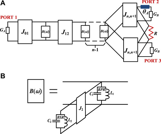
FIGURE 1. (A) Topology of nth-order dual-band FPD. (B) Inverter-coupled resonator sections B(ω).
Analysis of Filtering Power Division Response
On the bias of the frequency transformation and prototype synthesis technique, the prescribed dual-band filtering power division response can be obtained step by step. In the first step, the admittance of inverter-coupled resonators in Figure 1B viewed from the input/output is derived by:
where ω0i and bi represent the angular resonant frequency and susceptance slope parameter of the ith resonator, respectively.
Assuming that the FPD has two passbands of (ωL1, ωH1) and (ωL2, ωH2), the lower limits of the two passbands (ωL1, ωL2) ought to map to −1 in the normalized domain, while the upper limits (ωH1, ωH2) ought to map to +1 in the normalized domain. The parameters that define the transformation (ω01, ω02, b1, and b2) can finally be expressed as the functions of the two passband limits (ωL1, ωH1, and ωL2, ωH2) according to the relationship between the roots and the coefficients of the equation of T(ω) = 1. Since the function U(ω) = T(ω)-1 denotes the ratio of two polynomials, we can further use Q(ω) to represent the numerator of U(ω) as:
Once the aforementioned frequencies are prescribed according to specifications in advance, the parameters (ω01, ω02) and (b1, b2) can be calculated as:
Afterward, by mapping the nth-order dual-band FPD topology to its corresponding low-pass prototype, the inverters’ values can be finally expressed as [12]:
Afterward, the coupling coefficients between the adjacent BPRs can be derived as:
Meanwhile, the coupling coefficient between the BSR and BPR can be derived as:
In addition, the external quality factors can be formulated by:
After the dual-band filtering power division responses are analyzed, the isolation and phase distribution can be obtained by means of the isolation resistor R and the branch lines, respectively.
Analysis of Phase Difference Between Outputs
In order to analyze the phase difference between the output ports of the dual-band filtering power division network topology, the ABCD matrix of the whole circuit is solved through the microwave network analysis method. Furthermore, the insertion phase shifts ∠S12 and ∠S13 can be deduced.
First, ∠S12 is analyzed. Assuming that the incident wave is only introduced in port #1 and output in port #2 (GA = GB = Y0), the topology diagram of the dual-band filtering power division network with phase-shifting function in Figure 1A is appropriately simplified and redrawn, as shown in Figure 2. There are five sub-circuits in this schematic, as denoted by sub-circuit I, sub-circuit II, sub-circuit III, sub-circuit IV, and sub-circuit V.
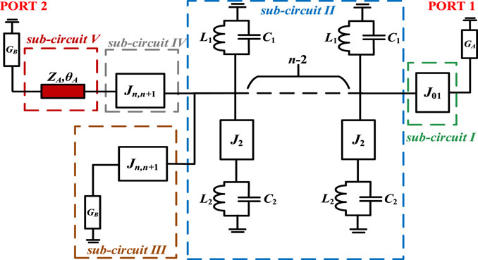
FIGURE 2. Equivalent circuit diagram for analyzing phase difference between two output ports.
For dual-frequency resonant units B(ω), its input admittance P can be represented as:
where P1 = jωC1 is represented as the square root of capacitances of BPR and BSR in the low-pass prototype, where the value of eac+1/jωL1, P2 = jωC2+1/jωL2, and P1 and P2 are the admittances of the corresponding resonators.
For sub-circuit I, its ABCD matrix can be obtained as:
For sub-circuit II, its ABCD matrix can be obtained as:
where
Meanwhile, for sub-circuits III, IV, and V, their ABCD matrix can be obtained, respectively, as follows:
Finally, the ABCD matrix of the whole circuit can be solved as follows:
where
Then, the insertion phase ∠S12 can be obtained as:
In a similar way, the insertion phase ∠S13 can be obtained as:
where
Once the phase shifts ∠S12 and ∠S13 are achieved, the phase difference between the output ports can be finally solved by subtracting the two equations (∠S12 and ∠S13). Furthermore, the desired electrical length of the branch line can be obtained.
Analysis of Isolation Between Outputs
After analyzing the phase difference between outputs, the isolation can also be derived by means of the microwave network analysis method [13]. First, assuming that the incident wave is only introduced in port #2 and output in port #3 (GA = GB = Y0), the topology diagram of the dual-band filtering power division network with phase-shifting function in Figure 1A is appropriately simplified and redrawn, as shown in Figure 3.
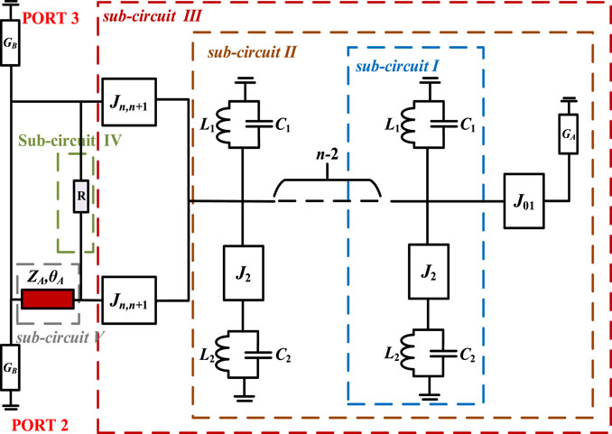
FIGURE 3. Equivalent circuit diagram for analyzing isolation between two output ports.
The equivalent circuit diagram has five sub-circuits, which are represented as sub-circuits I, II, III, IV, and V, respectively. As mentioned earlier, with the calculated admittance N1 of sub-circuit II, the ABCD matrix of sub-circuit III can be deduced as:
Then, we can attain the admittance matrix Y1 of sub-circuit III with the following equation by conveniently transforming the ABCD matrix to its corresponding admittance matrix:
In a similar way, the admittance matrix Y2 of sub-circuit IV can be derived as:
In the meantime, the ABCD matrix of sub-circuit V is shown as follows:
Then, the result of Y1 + Y2 should be converted into an ABCD matrix and cascaded with the ABCD matrix of sub-circuit V to find the whole ABCD matrix of the schematic that has been analytically derived as follows:
where
Till now, the scattering parameter S23 can be derived according to the conversion relationship between S parameter and transfer matrix, and then the isolation resistance R can be further obtained by setting S23 = 0. The solution formula of resistance R can be derived as follows:
where
When all the design parameters are known, the analytical solution of the required resistance R can be obtained through Eq. 16. In the next section, the microstrip E-shape resonator is chosen as the basic resonant element to design a dual-band filtering power divider with 90° phase distribution, which verifies the proposed design method.
Implementation and Results
To validate this design method, a dual-band FPD prototype was designed and fabricated based on the substrate of Rogers RO4003C with a relative dielectric constant εr = 3.55, thickness h = 0.508 mm, and loss tangent tan δ = 0.0027.
The L/C resonators are all implemented by E-shape resonators as shown in Figure 3A, and the external/internal couplings are all controlled through the gap couplings. Based on the aforementioned analytical equation, the required design parameters can be obtained.
For the E-shape resonators, it can be analyzed by means of even/odd-mode analysis, and the odd-mode and even-mode equivalent circuits are shown in Figures 4B, C. Based on the even/odd-mode analysis, the resonant frequency of the odd-mode and even-mode can be obtained as [14]:
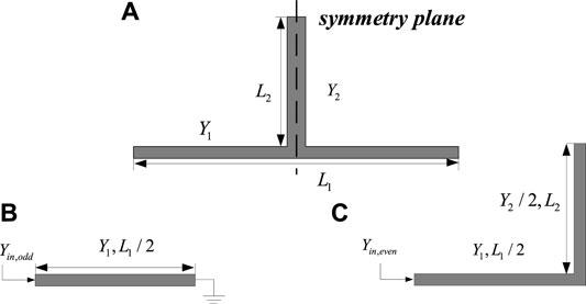
FIGURE 4. (A) Structure of the employed E-shape resonator. (B) Odd-mode equivalent circuit. (C) Even-mode equivalent circuit.
The odd-mode resonant frequency of two pairs of E-shape resonators is used to construct the dual-band filtering power divider.
The whole configuration of the proposed dual-band FPD including corresponding dimensions is shown in Figure 5. As observed, there are two pairs of dual-mode resonators between the input port and the output port. The lower pairs of dual-mode resonators are the bandpass resonators, while the upper pairs of dual-mode resonators are the bandstop resonators. The signal is introduced from port #1 and coupled to the arm of the first E-shape resonator. Then, the signal flows through the two pairs of E-shape resonators and is coupled to the two output ports (port #2 and port #3) by the arm of the second bandpass E-shape resonator, which forms a three-coupled line structure. Also, the isolation resistance R is loaded on the front end of the three-coupled line structure to achieve good port–port isolation.
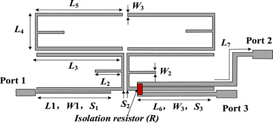
FIGURE 5. Configuration of the proposed dual-band FPD with physical dimensions: L1 = 16.5, L2 = 8.5, L3 = 17, L4 = 7.65, L5 = 17.9, L6 = 16.3, and L7 = 24, W1 = 0.36, W2 = 0.3, and W3 = 1.1, S1 = 0.1, S2 = 0.3, and S3 = 0.1 (all units: mm), and R = 195Ω. The design targets of the proposed dual-band FPD are given as follows: 1) Passbands 1: 1.87–1.92 GHz; 2) Passbands 2: 2.06–2.11 GHz; 3) Return loss: 20 dB; 4) Isolation: >20 dB; 5) Phase distribution: 90°.
In addition, Figures 6A, B exhibit the simulated and measured results of the proposed dual-band FPD. As shown in Figures 6A, B, the measured insertion losses are 1.2 and 1.3 dB, respectively, the measured return losses are all higher than 18 dB, and the measured in-band isolation within two output ports is all higher than 16 dB. Moreover, the phase difference between two outputs within the two passbands is about 90° with less than 3° phase imbalance. The photograph of the fabricated circuit board of the dual-band FPD is shown in Figure 7. The overall size of the circuit is 0.67λg × 0.53λg, where λg is the relative wavelength of the center frequency. In conclusion, the decent results exhibit the feasibility and effectivity of our proposed design method.
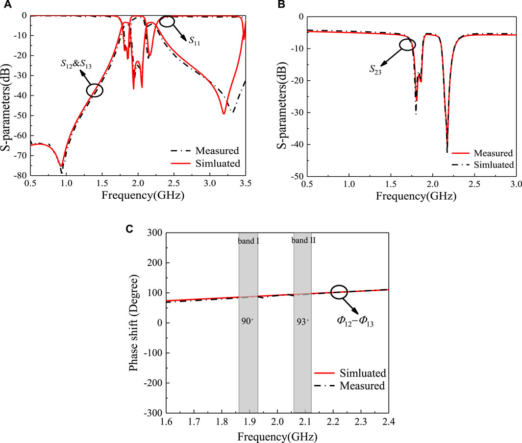
FIGURE 6. Measured and simulated results of the proposed dual-band FPD. (A) Magnitudes of S11, S12, and S13. (B) Magnitudes of S23. (C) ∠S12−∠S13.
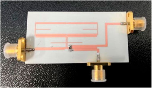
FIGURE 7. Photograph of the fabricated circuit board.
Conclusion
This study presented a novel synthesis design method of dual-band FPD including arbitrary phase distribution based on the topology of inverter-coupled L/C resonators. A representative dual-band FPD with 90° phase distribution based on E-shape resonators has been designed and fabricated to verify the design method. It is our belief that the proposed method will be very attractive in future multi-functional wireless communication systems.
Data Availability Statement
The original contributions presented in the study are included in the article/Supplementary Material, further inquiries can be directed to the corresponding author.
Author Contributions
JS, WL, KP, ZZ provide the idea and write the paper. MS modify the paper.
Conflict of Interest
The authors declare that the research was conducted in the absence of any commercial or financial relationships that could be construed as a potential conflict of interest.
Publisher’s Note
All claims expressed in this article are solely those of the authors and do not necessarily represent those of their affiliated organizations, or those of the publisher, the editors, and the reviewers. Any product that may be evaluated in this article, or claim that may be made by its manufacturer, is not guaranteed or endorsed by the publisher.
References
1. Wang K-X, Zhang XY, Hu B-J. Gysel Power Divider with Arbitrary Power Ratios and Filtering Responses Using Coupling Structure. IEEE Trans Microwave Theor Techn (2014) 62(3):431–40. doi:10.1109/tmtt.2014.2300053
2. Chau W-M, Hsu K-W, Tu W-H. Filter-based Wilkinson Power Divider. IEEE Microw Wireless Compon Lett (2014) 24(4):239–41. doi:10.1109/lmwc.2014.2299543
3. Chen C-J, Ho Z-C. Design Equations for a Coupled-Line Type Filtering Power Divider. IEEE Microw Wireless Compon Lett (2017) 27(3):257–9. doi:10.1109/lmwc.2017.2661968
4. Bai YC, Xu. KD. High-performance Filtering Power Divider with Multiple Transmission Zeros. Microw Opt Technol Lett (2018) 60(11):2673–6. doi:10.1002/mop.31468
5. Xu KD, Bai Y, Ren X, Xue Q. Broadband Filtering Power Dividers Using Simple Three-Line Coupled Structures. IEEE Trans Compon., Packag Manufact Technol (2019) 9(6):1103–10. doi:10.1109/tcpmt.2018.2869077
6. Yu W, Xu L, Zhang XY, Chen J-X. Dual-band Dual-Mode Dielectric Resonator Filtering Power Divider with Flexible Output Phase Difference and Power Split Ratio. IEEE Trans Microwave Theor Techn. (2022) 70(1):190–9. doi:10.1109/tmtt.2021.3113654
7. Hong W, Jiang ZH, Yu C, Zhou J, Chen P, Yu Z, et al. Multibeam Antenna Technologies for 5G Wireless Communications. IEEE Trans Antennas Propagat (2017) 65(12):6231–49. doi:10.1109/tap.2017.2712819
8. Basavarajappa V, Pellon A, Montesinos-Ortego I, Exposito BB, Cabria L, Basterrechea J. Millimeter-wave Multi-Beam Waveguide Lens Antenna. IEEE Trans Antennas Propagat (2019) 67(8):5646–51. doi:10.1109/tap.2019.2916388
9. Lyu Y-P, Zhu L, Cheng C-H. A New Design of Filtering Power Dividers with Arbitrary Constant Phase Difference, Impedance Transformation, and Good Isolation. IEEE Access (2019) 7:169495–507. doi:10.1109/access.2019.2955104
10. Kim S, Chaudhary G, Jeong Y. Filtering Power Divider with Arbitrary Prescribed Phase Difference. In: 2020 IEEE Asia-Pacific Microwave Conference (APMC) (2020):421–3.
11. Zhu X, Yang T, Chi P, Xu R. Miniaturized Reconfigurable Filtering Power Divider with Arbitrary Output Phase Difference and Improved Isolation. In: 2021 IEEE MTT-S International Microwave Symposium (IMS) (2021):104–7.
13. Lee B, Nam S, Lee J. Optimization-free Design Equations for Narrowband Equal-Division Filtering Power Divider with Pre-specified Filtering Response and Wideband Isolation. IEEE Trans Circuits Syst (2019) 66(7):2496–507. doi:10.1109/tcsi.2019.2898465
Keywords: direct synthesis design, filtering power divider, dual-band, phase distribution, isolation
Citation: Shen J, Li W, Ping K, Zhang Z and Shu M (2022) Synthesis Design of Dual-Band Filtering Power Dividers Based on E-Shape Resonators. Front. Phys. 10:907718. doi: 10.3389/fphy.2022.907718
Received: 30 March 2022; Accepted: 11 April 2022;
Published: 09 May 2022.
Edited by:
Kai-Da Xu, Xi’an Jiaotong University, ChinaReviewed by:
Baoping Ren, East China Jiaotong University, ChinaZhi-Chong Zhang, Jinggangshan University, China
Copyright © 2022 Shen, Li, Ping, Zhang and Shu. This is an open-access article distributed under the terms of the Creative Commons Attribution License (CC BY). The use, distribution or reproduction in other forums is permitted, provided the original author(s) and the copyright owner(s) are credited and that the original publication in this journal is cited, in accordance with accepted academic practice. No use, distribution or reproduction is permitted which does not comply with these terms.
*Correspondence: Zhuowei Zhang, emh1b3dlaV96aGFuZ0AxNjMuY29t