 Iris Cusini*
 Davide BerrettaEnrico ConcaAlfonso Incoronato
 Francesca MadoniniArianna Adelaide MaurinaChiara NonneSimone Riccardo
 Federica Villa
- Dipartimento di Elettronica, Informazione e Bioingegneria, Politecnico di Milano, Milano, Italy
The ability to detect single photons is becoming an enabling key capability in an increasing number of fields. Indeed, its scope is not limited to applications that specifically rely on single photons, such as quantum imaging, but extends to applications where a low signal is overwhelmed by background light, such as laser ranging, or in which faint excitation light is required not to damage the sample or harm the patient. In the last decades, SPADs gained popularity with respect to other single-photon detectors thanks to their small size, possibility to be integrated in complementary metal-oxide semiconductor processes, room temperature operability, low power supply and, above all, the possibility to be fast gated (to time filter the incoming signal) and to precisely timestamp the detected photons. The development of large digital arrays that integrates the detectors and circuits has allowed the implementation of complex functionality on-chip, tailoring the detectors to suit the need of specific applications. This review proposes a complete overview of silicon SPADs characteristics and applications. In the previous Part I, starting with the working principle, simulation models and required frontend, the paper moves to the most common parameters adopted in literature for characterizing SPAD performance and describes single pixels applications and their performance. In this Part II, the focus is posed on the development of SPAD arrays, presenting some of the most notable examples found in literature. The actual exploitation of these designs in real applications (e.g., automotive, bioimaging and radiation detectors) is then discussed.
Single-Photon Avalanche Diode Arrays
Single-Photon Avalanche Diodes (SPADs) are p-n junctions biased above their breakdown voltage. In this operation modality, namely Geiger mode, contrary to the analog/linear behavior of Avalanche Photodiodes (APDs), the output is a digital signal not proportional to the number of impinging photons [1]. Indeed, when a photon is absorbed in the multiplication region of a SPAD, a self-sustaining avalanche can be generated. This intrinsic positive feedback causes the current to increase rapidly to a macroscopic level allowing single-photon sensitivity and to mark with picoseconds time resolution the arrival time of the detected photon. Each detection is followed by a deadtime, required for quenching the avalanche and resetting the SPAD, during which the sensor is blind. SPADs main characteristics a thoroughly analyzed in Part I of this review.
SPADs, both as single detectors and in multi-pixel configurations, are exploited mainly using three approaches: Single-Photon Counting (SPC), photon-timing through dedicated timing electronics, and time-gated SPC. In SPC, the intensity of slowly varying optical signals (in the μs range) can be acquired by counting photons in real-time. Fast varying optical waveforms (in the ps range) can instead be reconstructed through the Time-Correlated Single-Photon Counting (TCSPC) technique. TCSPC requires to record a sufficiently high number of measurements (cycles) of the arrival time of individual photons (photon-timing) to build the histogram of arrival times versus number of detected photons. Indeed, usually SPADs cannot be used as single-shot sensors in TCSPC acquisitions since they can provide only one time of arrival per cycle. By accumulating the arrival times over multiple cycles, the waveform of the incoming signal is reconstructed allowing, for example, to identify a laser peak against the background or to measure fluorescence decaying times.
The detection events can be time-stamped either by coupling the SPAD with a Time to Digital Converter (TDC) or by counting the photon detected in narrow integration windows (gate windows) with different delays (time-gated SPC) [2].
Time-gated SPC allows reconstructing the waveform of fast optical signals by using a sliding-time window scheme: the waveform of the input signal is sampled by “sliding” the delay of the integration window. Gating can be applied by masking any avalanche that is generated outside well-defined time intervals (namely soft-gating) or by depolarizing the SPADs below breakdown (namely hard-gating). The possibility of turning on and off SPADs in a few hundreds of picoseconds allows the exploitation of fast gated counting in applications which demand to time-filter the incoming optical signal [3, 4].
Single SPAD pixels have found extensive use in both SPC and TCSPC [5, 6]. However, in many fields, the possibility of acquiring multiple spots in parallel is strongly advantageous since it reduces the measurement time and allows to use none or simpler scanning mechanisms. Thus, since the end of the last century, a big effort has been placed into the development of multi-SPAD chips. Starting from small arrays that integrate only SPADs connected to discrete-components electronics [7], in 2003 the first example of an array implementation in standard Complementary Metal-Oxide Semiconductor (CMOS) technology was presented [8].
Note that, combining different SPAD pixels in close proximity inevitably causes optical crosstalk between the different photodetectors. Indeed, hot carriers flowing through a triggered SPAD emit secondary photons which may initiate a multiplication process in neighboring SPADs. Optical crosstalk can be reduced by minimizing the avalanche charge per pulse, by placing absorption media among pixels, such as highly doped isolation diffusions or deep trench isolation, and by increasing the pixels pitch. Crosstalk probability between two pixels can be measured by building a histogram of the two pixels inter-arrival times. The spurious coincidences expected in the absence of crosstalk can be estimated from the histogram and subtracted leaving only the events caused by crosstalk, which are then divided by the total number of events for obtaining the crosstalk probability [9].
Having the possibility to combine SPADs and electronics in the same chip, the natural evolution of SPAD arrays has been the integration of the needed auxiliary circuits for signal processing (such as TDCs and counters) together with the detectors. Different design strategies have been proposed according to the requirements of the specific application. Figure 1 summarizes the most common configurations. The starting point is an array of simple pixels made up of a SPAD and its frontend circuit (Figure 1A). Then, the processing circuits can be integrated into the pixel (Figure 1B) to perform specific functions, allowing parallel independent operation of each SPAD pixel. In order to mitigate the effect of the intrinsic SPAD deadtime and to gain photon-number resolution, it is also possible to include multiple SPADs and their frontend circuits in each pixel (Figure 1C). In this case, the outputs from the different SPADs are combined before being processed in-pixel. Pixels constituted by many SPADs are often named digital Silicon Photomultipliers (dSiPM). According to the specific application, the in-pixel processing can be triggered either by each ignited SPAD (combinational OR logic), or only if a number of SPADs higher than a set threshold are ignited at the same time (combinational AND logic). Multiple dSiPMs can be then combined in an array as in Figure 1D.
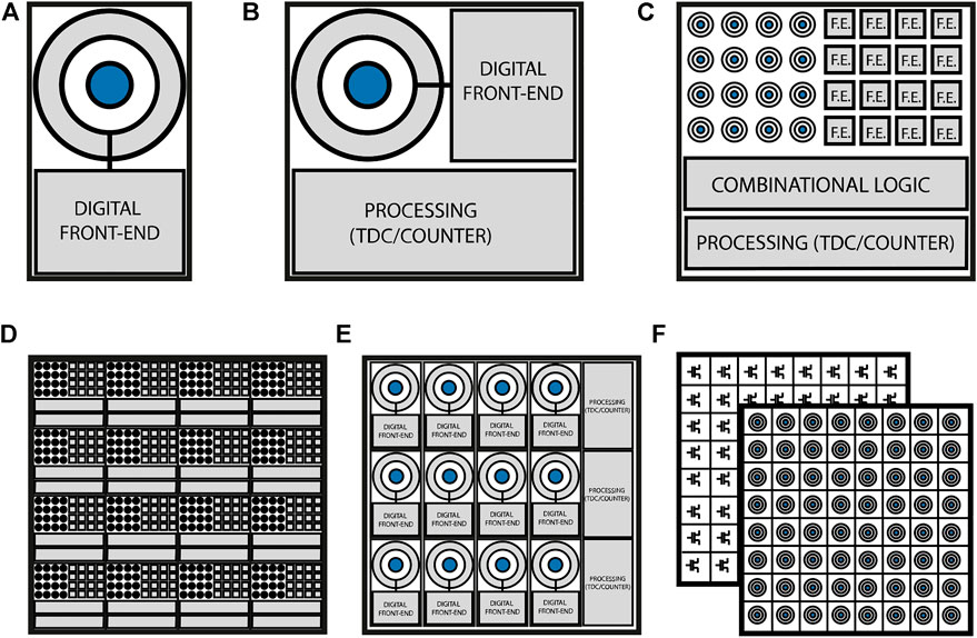
FIGURE 1. Schematic representations of a pixel integrating a SPAD and its frontend (A), a pixel that also includes the electronics for signal processing such as TDCs or counters (B), a dSiPM (C), an array of dSiPM (D), a SPAD array with row-level logic (E), and a 3D stacked array (F).
The major drawback in integrating advanced features in a pixel is the loss of active area. Indeed, a fundamental parameter of SPAD arrays is the Fill-Factor (FF), defined as the active area over the pixel area. The Photon Detection Efficiency of a SPAD array, i.e. the overall pixel efficiency, is then defined as
FF can also be recovered by mounting on top of the chip a microlens array (MLA) in which each lens collects photons from the entire pixel area and conveys them to the SPAD active area. Microlenses can significantly improve the effective PDE, mostly when collimated light beams are employed [10, 11]. However, using MLAs, especially for high pixel number arrays, substantially increases the complexity and the cost of the system. Recently, 3D-stacked technologies have been providing an excellent tool to preserve FF even with in-chip complex electronics. In vertically integrated sensors, the top tier houses the SPADs, while the bottom tier integrates the electronics (Figure 1F). In this way, the pixel geometry is optimized and the use of two different technologies for the two tiers, taking advantage of low-power and scaled down nodes for the bottom one, becomes possible.
Another fundamental aspect of SPAD arrays is their readout mode, which strongly influences the chip performance in terms of frame rate and maximum count rate. Typically, SPAD arrays employ global-shutter readout modes, exposing all the pixels simultaneously, while buffering can be utilized to simultaneously acquire a new frame and readout the previous one, to preserve a high frame rate. Sharing resources, either between pixels or at array or column level, speeds up the readout since it reduces the amount of data produced by the chip. Integrating the post-processing on-chip (e.g., on-chip histograms or coincidences detection) strongly reduces the amount of data that needs to be readout, either shortening the readout time or lowering the required data throughput. Regardless of the configuration of choice, the readout can be either frame-based (i.e., after each frame window, the data from the entire array are read) or event-driven (i.e., the readout is triggered by an event such as the detection of a photon coincidence or a threshold overrun). The convenience of one approach in respect to the other mainly depends on the detector count rate. For high-count rate applications, when most of the pixels are triggered during the frame time, the frame-based approach is the best one, instead for photon starved applications, event-driven approaches are preferred since in this case the addresses of triggered pixels are provided, avoiding to readout lots of useless information.
The following Sections offer a brief overview of the main categories of SPAD arrays, distinguishing them in linear arrays, planar arrays, and 3D-stacked arrays, while Table 1 compares some of the most significant SPAD arrays presented in literature. For each array first author with reference, publication year, and affiliation of the first author are reported. The following parameters are also indicated: employed technology, pixels number, number of SPADs per pixel, SPAD pitch, peak PDP and corresponding wavelength, FF, DCR/area, and maximum frame rate. Since most of the arrays include processing on-chip it is also indicated if counters for SPC are present, and in case the number of bits, in case it operates in gated mode, the type of gating (Soft or Hard), TDC resolution, and histogram bins number. Finally, the main application for which the array has been designed is reported.
TABLE 1. Main SPAD parameters and counting and timing figures-of-merit for several SPAD arrays described in literature.
Linear Arrays
First CMOS SPADs linear arrays started to appear in the early 2000s, straight after the firsts SPADs integrated in CMOS technologies. The geometry of linear sensors allows to reach high FF even when complex frontend and processing circuitry are integrated for each SPAD, since the electronics is laid out on the side of the active region. Typically, linear arrays outperform planar arrays in terms of timing jitter (since frontend and timing electronics are not bound by pixel area limitations), crosstalk (which is only due to the two adjacent pixels), and readout speed (given the relatively low number of pixels).
The first linear arrays were developed at the Ecole Polytechnique Fédérale de Lausanne, and published in 2006 and 2007 respectively by Niclass [12] and Sergio [13]. The former, mainly designed for counting applications, is a 112 × 4 array, which provides the addresses of the triggered pixels with an event-driven readout approach. The latter includes 128 × 2 pixels with a 1-bit register to keep track of the triggered pixels for counting applications, and a timing-preserving delay line, with different delays for each pixel, enabling photon timing applications. Both these arrays are general purpose and do not perform any processing on-chip, indeed both photon counting and timing are performed off-chip through FPGA or other dedicated instrumentation.
Over the years, SPAD arrays started to be designed for specific applications, developing on-chip processing. In particular, linear arrays are attractive for spectroscopy applications, such as Raman Spectroscopy (RS) and time-resolved emission spectroscopy, since the spectral information can be mapped in different pixels of the array.
Since the early stages of linear SPADs arrays, time-gated SPC has been implemented on-chips, both with the purpose of retrieving timing information about the decay time in Fluorescence Lifetime Imaging (FLIM) and of time-filtering the incoming light to reject unwanted contributions (e.g., fluorescence light in RS). Examples of linear arrays implementing gated counting are Pancheri [14], Murayama [15], and Nissinen [16]. Gating can be applied at the SPAD level (hard gating), or only at the counter level (soft gating), allowing only the SPAD pulses within the gate window to trigger the counter. Pancheri and Stoppa developed at the Fondazione Bruno Kessler (FBK) a 64 × 4 array [14], exploiting the principle of time-gated fluorescence lifetime detection, evaluating light intensity in four different gate windows. Soft gating has been implemented in this structure thanks to a toggle flip-flop where the SPAD output signal is connected to the clock input, whereas the time window toggles input. The output pulses increment an 8-bit ripple counter whose output is then transferred to a Shift Register for the final readout. Muruyama [15] presents two different 1024 × 8 array for RS and Laser Induced Breakdown Spectroscopy (LIBS), both with soft and hard gating, a 1-bit counter, and readout interface circuit per pixel. In type I circular SPADs have been used, whereas in type II, to improve PDE, large square-shaped SPADs have been employed, additionally to a separate independent power line to increase excess bias. A time gated 2 × 4 × 128 array for Raman has been proposed by Nissinen [16] with an adjustable time-gate width in the sub-nanosecond range. In this architecture, both hard and soft gating are implemented thanks to an off-chip delay generator producing eight signals. Four are used to actively control the biasing of the SPADs, the other four are used by the arbiters to compare the arrival times of the gate signals with the SPADs output. The output is then fed to the counters and finally transferred to the FPGA controller.
About one decade after the first linear arrays, detectors including on-chip TDCs to time-stamp the incoming photons were presented. The first example was published in 2013 by Niclass [17], for Light Detection and Ranging (LiDAR) applications. It includes 32 × 1 pixels with 12 SPADs and a 208 ps TDC per pixel, while the timing histogram is processed in FPGA. Both photon timing (250 ps resolution) and photon counting (6-bit) are allowed by the 60 × 1 array presented in Villa [18]. More sophisticated architectures allow for both time gating and photon timing, such as the 256 × 2 by Krstaji [19] (350 ps resolution, hard gating), the 4 × 128 by Nissinen [20] (78 ps resolution, hard gating), later extended to 256 × 16 [21] (50 ps resolution, soft/hard gating), and the 128 × 1 by Conca [5] (260 ps resolution, hard gating). In order to decrease the amount of data to be readout and processed off-chip, the timing histogram can be computed on-chip, for each pixel, as in Krstaji [19], Erdogan [22, 23] and Seo [24], consequently increasing the maximum count rate in respect to arrays that integrates only TDCs. An opposite approach is presented in Burri [25], where all the processing is performed on a dedicated FPGA, and the linear array includes only the 256 × 1 SPADs and their frontend circuits, in order to separately maximize the SPAD and timing performance and to favor the system flexibility.
With the aim of optimizing performance, the 32 × 1 array by Cuccato [26] has been developed by bonding together an array of SPADs fabricated in custom technology and an array of Time-to-Analog Converters (TACs) fabricated in a 0.35 SiGe BiCMOS technology.
A two-chip structure has been also proposed by Renna in its 16 × 1 array [4], fabricating SPADs and Active Quenching Circuits (AQCs) in two different technologies: the 0.35 μm HV CMOS by Fraunhofer IMS is used for low-noise SPADs production, whereas the 0.35 μm SiGe-BiCMOS process guarantees better frontend and timing performance. An AQC array based on a differential readout (SPAD and dummy) is here proposed for fast gating purposes, with few improvements to decrease the number of external connections.
Finally, a peculiar architecture has been recently proposed by Incoronato [27]. It is a 32 × 1 array, designed for a Quantum Random Number Generator (QRNG) system on-chip. This architecture allows both single-photon detection and on-chip evaluation of coincidence detections.
Planar Arrays
The evolution in technological processes and the growing request in many applications for more sophisticated single-photon detection systems paved the way to the design of dense smart planar arrays. These sensors feature a 2D layout, so the SPADs are arranged by rows and columns. Of course the first advantage is the possibility to enhance the collecting area and resolve two dimensions as in classical Charge-Coupled Devices (CCD) and CMOS Active Pixel Sensors (APS) sensors. Differently from linear arrays, where the SPAD frontend and processing electronics is laid out outside the active region without affecting FF, in large planar arrays frontend and processing have to be integrated within the pixel area, with detrimental effects on the FF. For this reason, in some applications, where the detection efficiency needs to be maximized, MLAs can be added on top of the SPAD array [28, 29] recovering the wasted lights due to the surrounding electronics. Large arrays also require a reliable signal distribution to the whole matrix, especially for fast clocks needed in timing circuits, therefore clock trees and buffers are distributed along the array increasing power consumption.
The first integrated planar array ever realized is a 4 × 8 by Rochas [8] in 2003. This array has been fabricated in an 800 nm CMOS technology node, each SPAD is quenched passively by a resistor and a simple inverter is used as comparator. No further electronics has been added on-chip, and the outputs of four pixels are provided externally through a multiplexer. This architecture shows a 20% peak PDP and less than 1% FF. Arrays with low pixel number and direct outputs have been proposed also more recently, (e.g., by Gösch [30] and Buttafava [31]), and find use in some applications because of their flexibility and event-driven readout. With higher number of pixels, having one output for each SPAD is no more possible, thus arrays featuring Address-Event Representation (AER) readout (i.e. providing just the digital pulse corresponding to the photon arrival and the pixel address) have been proposed by Berkovich [32] (20 × 20 pixels) and Niclass [33] (64 × 48 pixels).
In order to implement the TCSPC technique exploited in many applications, some timing electronics has been added in the chips. Indeed, many arrays embed multiple TDCs1 [34, 35, 36] that compute and store the Time-Of-Flights (TOFs) in a buffer memory. The 64 × 64 by Schwartz [37] in 2007 features one TDC every SPAD with 350 ps coarse time resolution, plus a multiphase clock interpolator in a 350 nm HVCMOS technology. The 32 × 32 by Richardson [38] in 130 CIS technology achieve 50 ps resolution and 1 Mfps readout. More general architectures have been proposed, with both timing and counting electronics to achieve great versatility in the final application (e.g., Villa [39] and Manuzzato [40]). In the 192 × 128 array by Henderson [29], realized in a 40 nm technology, every pixel can take advantage of a 33 ps resolved TDC and an 8-bit counter. In the 160 × 120 by Perenzoni [41] an analog counter is proposed, resulting in a very compact 7-transistors (7T) pixel architecture.
As the resolution increases, it is very hard to have dedicated logics for each SPAD, so some sharing techniques need to be introduced, as in Niclass [42] and Braga [43] with a column based TDC sharing technique or Carimatto [44] where 128 TDCs are shared among 128 × 128 pixels. The 32 × 32 array by Zhang [45] shares 4 TDCs among a column of 32 pixels, while in the 16 × 16 by Riccardo includes 16 TDCs, each one shared by 16 SPADs [46]. Another example of sharing is the 32 × 128 by Jahromi [47] for 3D imaging, where only two columns (clusters of 2 × 128 SPADs) are illuminated by blade laser shape at each frame, thereby 257 TDCs are connected to the used columns, drastically reducing the silicon area. Of course the cost is a more complex light emitting component, in which 16 laser diodes are turned on synchronous with the frame. Other timing electronics solutions can be embedded as in Parmesan [48] where a 256 × 256 imager implements TACs with a global ramp voltage and a column shared flash analog-to-digital converter, with an overall 6.6 ps resolution.
Within dSiPMs, SPADs can be connected with different logics, depending on the purpose. For example, XOR logic gates have been used in the 64 × 64 by Perenzoni [49], in which every pixel contains 8 SPADs connected to the same TDC. The dSiPM proposed by Conca [50], instead, connects 1782 SPADs through a pseudo nMOS OR gate, thus the TDC gets triggered and provides a TOF, as soon as a photon hits the dSiPM sensitive area. This SiPM aims at maximizing the collecting area for Time-Domain Near-InfraRed Spectroscopy (NIROT) application (i.e., in photon starved regime). SiPM approach can be also used when high-count rate is required, such as in Positron Emission Tomography (PET), as shown for instance in [36].
In photon starving application it could be useful to avoid the readout of the entire array improving the maximum achievable frame rate, thereby smart solutions, as in the 32 × 32 by Gasparini [51], are proposed. A control logic detects the pixels that did not present any event in the previous frame and skips the readout of them to reduce the number of data to be transmitted. In a second operation mode, if less than a set number of photons have been detected, the readout does not start at all skipping the frame.
Other timing techniques based on gated-counting employ different electronics, as signal generators or fast circuits to provide small observation windows and event counters to obtain the number of photons detected in that specific time window as in [52] by Burri. In 2009, a 60 × 48 array has been designed by Niclass [53] for Continuous Wave indirect TOF (CW-iTOF), here two counters per pixel detect the intensity in one semi-period, with 5-ns gate window. In the 72 × 60 array by Lee [54], a 10-bit counter is used along with a signal generator to perform 10 ns sliding gate windows at 72 ps steps. Bronzi [2] designed a 64 × 32 CW-iTOF sensor with three 9-bit counters per pixel, able to count in well-defined time gates.
Recently, some sensors have increased the on-chip resources and processing power to provide less raw data, especially in LiDAR applications, where many TOFs per pixel should be readout at every frame. These new arrays present histogram builders that accumulate the TDC conversions and provide the histogram peak, drastically reducing the readout time and the external processing. Many solutions have been designed with the purpose of reducing the per-pixel electronics, still maintaining precise temporal resolution. Kim [55] and Seo [56] in collaboration with Samsung, propose imagers with such on-chip smart processing and histogramming, obtaining good performance. The main drawback in a full histogram reconstruction is the big memory area required to achieve fine resolution and long range. A partial histogram (PH) solution can be implemented, by finding the coarse bin corresponding to the laser peak and then reconstructing a fine histogram around it. In the 252 × 144 array by Zhang [57], 72 partial histogram builders are used to find the peak in 3 steps, and finally the partial histogram of 16 bins is acquired around the peak with 48 ps resolution, achieving both long Full-Scale Range (FSR) and fine resolution with a moderate storage footprint.
As expected, planar arrays have a limit in the resolution and on-chip resources, and it is very challenging to achieve a very high number of pixels with complex processing electronics. In 2019 Ulku [58] proposed a 512 × 512, embedding no processing on chip, but just 1-bit memory and gating operation mode. The 11T pixel shows a 10.5% FF. In 2020, Morimoto [59], in collaboration with Canon, produced instead a 1024 × 1000 array, with 13% FF and two types of small pixels, 7T and 5.75T topologies. This very dense array can be employed in gated-counting applications, with a memory cell that stores the SPAD state in the gate window. Due to the big dimensions no timing or extra electronics is added, so direct TOF measurements can be performed only by sliding small gating windows.
As this brief discussion has shown, through the years, SPAD performance has attracted companies that have started to propose these sensors in industrial applications. The intensive design and investments on these devices have led to high end products, with improved performance with respect to research projects, thanks to remarkable technology processes.
3D-Stacked Complementary Metal-Oxide Semiconductor Single-Photon Avalanche Diode Sensors
The latest trend in SPAD arrays design, driven by research and, more recently, by commercial interest of large companies, is to move towards 3D integration. Extending the design of integrated circuits towards the third dimension proves to be extremely effective to achieve higher integration density and lower power consumption. This is especially beneficial for image sensors where a conventional planar approach requires to share the area between photon collection and processing electronics, while stacked arrays allow better area efficiency, dedicating the upper tier of the stack to photon detection, and the lower tier for processing and additional functionalities. An additional benefit of a stacked approach is the option to exploit different technologies for the sensor tier and for the bottom processing electronics, allowing to optimize the performance of the detectors and to exploit conventional CMOS processes for the digital part.
Stacked SPAD sensors, like conventional CMOS Image Sensors, can adopt either Front-Side Illumination (FSI) or Back-Side Illumination (BSI) [60]. Generally, the BSI approach is preferable thanks to the possibility of optimizing the optical interface by adding anti-reflection coatings, microlenses and even color filters; furthermore, BSI SPAD sensors often offer higher detection efficiency at longer wavelengths. FSI SPAD sensors typically employ a SPAD device structure more akin to the planar SPAD arrays, which may be suitable if detection efficiency at shorter wavelength is important (for example, as detectors in PET and FLIM), thanks to the low thickness of the neutral region above the SPAD depleted region. Figure 2 represents, schematically, the typical structure of an FBI and a BSI array.
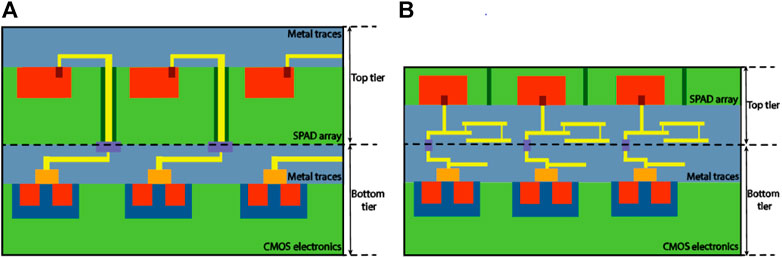
FIGURE 2. Schematic representations of an FSI 3D-stacked array (A), and a BSI 3D-stacked array (B).
FSI SPAD arrays rely on Through Silicon Vias (TSVs) [61], which allow to connect the metal layers of the top tier to the bottom tier. TSV manufacturing processes can be implemented either as a “via first”, where the vias are patterned and implemented at the very beginning of the Front-End-Of-Line (FEOL) process, before the transistors and other devices are created, as a “via middle”, where vias are created after the end of the FEOL processes, but before implementing the metal interconnects, or as a “via last”, where vias are created at the very end of the process flow. This last option allows to implement TSVs also as a post-fabrication step.
BSI SPAD arrays instead bond the metal interconnects of the two chips by flipping the SPAD tier onto the electronics side, after the creation of small copper pillars on top of the metal layers of each tier. The bonding is realized via Cu-Cu bonds, oxide-to-oxide bonds or a combination of the two in what is usually referred to as hybrid bonding (also referred to as Direct Bond Interconnect, DBI®) [62, 63]. Generally, this approach allows a higher interconnect density compared to TSVs.
The first demonstration of a 3D-stacked SPAD sensor dates back to 2006. Such sensor, reported in Aull [64], consisted in a 64 × 64 SPAD array and relied on a three-tier stacking to combine SPADs developed in a custom technology, a 0.35 μm 3.3 V SOI layer and finally a 0.18 μm 1.5 V tier. This approach allowed the authors to combine the high voltage tolerance of the 0.35 µm technology, useful for SPAD frontend, with the density offered by the 0.18 μm digital circuitry to implement a time-resolved Single-Photon Detector (SPD) with a pixel pitch of 50 μm, a remarkable achievement for the time. Stacking was enabled by TSVs with a diameter of 1.5 μm and low-temperature oxide-to-oxide bonding.
The first two-tier linear SPAD array sensor was presented by the group at EPFL in Mata Pavia 2015 [65]. This sensor relied on 130 nm technology both for the electronics and for the SPAD tiers, stacked by means of copper-to-copper DBIs, and allowed the authors to achieve an 11 μm detector pitch with an FF of 23.3% exploiting BSI. This detector was optimized for optical tomography, featuring 100 TDCs with a 49.7 ps resolution, each shared among a group of 4 SPADs.
In Al Abbas [66], the group at University of Edinburgh reported a 128 × 120 SPAD array for microendoscopy with the stacking of a 90 nm SPAD tier and an advanced 40 nm node for the electronics, allowing the on-chip integration of a synthesized microcontroller and SRAM memory banks to implement signal pre-processing and compression. This chip achieved time-resolving capabilities by implementing time-gated SPC, allowing the extraction of fluorescence lifetimes.
The same group also presented a larger 256 × 256 SPAD array in Hutchings [67], specific for Flash LiDAR and implementing a novel SPAD grouping approach. This allowed the authors to implement a variety of operation modes, adding to conventional TCSPC operation a novel in-pixel histogramming proposed for LiDAR. A similar approach to 3D-stacked SPAD sensor, implementing TDC sharing and histogramming, but also including a partial histogram readout to reduce data throughput, was later presented by Adaps Photonics [68].
Recently, the group at EPFL published papers presenting two different approaches to 3D stacking, but with a similar global architecture pairing multiple SPADs to a single TDC. One detector, reported in Ximenes [69], with a combination of a BSI top tier in 45 nm CIS technology paired to a 65 nm logic bottom tier, put the emphasis on integrating complex digital circuitry for LiDAR imaging, allowing the use of a moderate number of TDCs in a large array by means of a smart sharing circuit. Similarly, Padmanabhan [70] describes a 256 × 128 array for high background LiDAR combining coincidence detection and time-gating. Differently, Gramuglia [71] presents a sensor designed for TOF PET imaging which made use of two 0.18 μm tiers paired via TSV and microbumps, allowing the SPADs to be front-illuminated and enhancing the detection efficiency at shorter wavelengths. The bottom tier hosts high-resolution TDCs and addressing logic, exploiting a selective readout to minimize read operations of invalid data.
A major acceleration in the development of 3D-stacked SPAD arrays was set by the decisive entrance of major imaging companies into the SPAD array field, who presented various SPAD arrays featuring sub-10 μm SPAD pitch, high detection efficiency and built-in microlenses to further enhance light harvesting capability. The major markets driving these efforts are LiDAR, short-range 3D imaging and security. All the sensors presented in these categories make use of BSI illumination and Cu-Cu interconnections to achieve the tight pitch.
Sony published in Kumagai [72] a 189 × 600 SPAD array in 90 nm SPAD/40 nm logic, developed for LiDAR, demonstrating remarkably high detection efficiency in the NIR (22% at 905 nm) and making use of SPAD clusters for coincidence detection and built-in Digital Signal Processing (DSP) blocks to process the timing information, allowing successful ranging beyond 150 m. A second sensor presented by the same company in Ogi [73] targets low-light imaging, exploiting the same technology to implement high frame rate color imaging over a large dynamic range, by dynamically combining SPC at low light levels with measuring the time required for overflowing the same counter at higher photon fluxes. The company, in Shimada [74], presented its new generation of stacked SPAD arrays, manufacturing the readout chip in 22 nm CMOS, reducing SPAD pitch to 6 μm and increasing detection efficiency beyond 30% at 905 nm.
Recently, Canon has focused its efforts at developing large-format SPAD arrays, breaking the 3 Megapixel barrier with a 6.39 μm pitch SPAD imager presented in Morimoto and Iwata 2021 [75], which is targeted for low-light imaging, thanks to a favorable combination of high detection efficiency (>69.4% at 510 nm) and low noise density (0.044 cps/μm2) SPADs, paired with a simple photon-counting bottom tier.
Single-Photon Avalanche Diodes Arrays Applications
Thanks to their single-photon sensitivity and precise timing resolution, nowadays SPADs and SiPMs are widely employed in TCSPC applications. Measuring distances through TOFs is a typical application in which SPADs are used exploiting the TCSPC technique. The first architectures presented in literature for TOF measurements used arrays of SPADs multiplexed to external TDCs, which measures the travel time of the emitted photons [76, 77]. The next generation of devices moved the timing circuits onto the same silicon die of the SPADs, allowing a much higher degree of scalability and a shorter acquisition time [42, 53]. In particular, LiDAR is an emerging technique based on the measurement of the travel time of a short laser pulse illuminating the scene to reconstruct 3D maps of the environments in long-range and real-time conditions. In 2013, Kagami’s digital SiPM array [17] has been one of the first ones to be specifically designed for LiDAR applications with particular focus on robustness to background light. Because of LiDAR applications in Autonomous Vehicles (AV) and Advanced Driver Assistance Systems (ADAS), industries became immediately involved in the research, starting from Toyota and STMicroelectronics. Those companies were the firsts to develop SPAD arrays including on-chip DSP [42]. Non-Line-Of-Sight (NLOS) imaging goes one step further, acquiring 3D images of objects outside the direct line of sight.
SPAD arrays and TCSPC technique are widely used in combination also in Biomedical and Biophotonics fields, which take advantage of single-photon detection and timing resolution. FLIM, RS and PET and radiation detection, in general, are just some of the most relevant examples. SPADs play a key role also in Quantum Information technologies, for quantum physics experiments, quantum communications and quantum imaging and microscopy.
The following Sections provide a more detailed description of the above-mentioned applications.
Light Detection and Ranging
Light Detection and Ranging (LiDAR) has attracted significant research and industrial interest in recent years as demands for 3D imaging have increased in various fields, including AV, ADAS, medical and consumer applications, biometric identification, security, and surveillance. Compared to other 3D imaging techniques, LiDAR typically uses laser light pulses (even if a promising approach called frequency-modulated continuous-wave LiDAR is taking on an emerging role [78]) instead of radar radio waves and sonar sound waves. Historically, the first LiDARs on the market were rotating LiDARs, which capture a wide Field Of View (FOV) at long ranges through scanning, but their components tend to be heavy and expensive, and the moving parts require regular maintenance. The general industry trend is moving from rotating parts to chip-based solutions without scanning (flash LiDAR) or with microscopic moving parts (based on Micro Electro Mechanical Systems—MEMS).
In pulsed-LiDAR, the TOF between emission and reception of laser echo pulse is measured, either by time-stamping the incoming photons arrival times through a TDC or by counting photons within gate widows progressively spanning across the FSR. Long timing electronics FSR is needed because, together with the laser power and the object reflectivity, it defines the achievable spatial FSR. For faster measurements, the TDC approach is convenient in most applications, since the detector is active during the entire FSR. TDC resolution or minimum feasible delay shift between gate windows define measurement resolution. Resolution and FSR can be traded-off depending on the application: high resolution at short range versus low resolution at long range [49]. The time resolution is critical since it influences the overall measurement precision by means of the quantization error. However, precision can be improved by acquiring more arrival times to build a histogram and computing the centroid over many repetitive measurements [79]. Figure 3 shows a typical pulsed-LiDAR system, which includes a pulsed laser, a time-resolved detector, and a post-processing unit for TOF extraction. SPAD arrays allow the on-chip integration of detectors, their frontends, time measurement circuits (e.g., TDC), and processing electronics (e.g., histogram circuitry), thus achieving compact real-time and reduced data-throughput LiDAR systems [24, 57, 67].
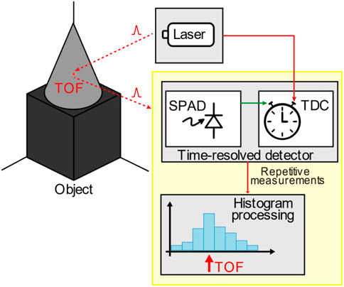
FIGURE 3. Schematic representation of a LiDAR system, with a pulsed laser (emitter), and a SPAD detector with TDC and histogram processing (receiver).
A first SPAD array figure of merit impacting LiDAR performance is the number of pixels, which indeed influence FOV, angular resolution, and measurement speed. A high pixel number is required for flash-LiDAR to capture the whole scene with no scanning elements. However, higher pixels number results in fewer photons per pixel, thus the need of repeating more times the acquisition to get enough signal. Dynamic Range (DR) is one of the most challenging detection requirements, especially when operating with strong background light (e.g., outdoor with solar illumination) and with different targets at different distances and with extremely variable reflectivity and light incidence angle. High detection efficiency and single-photon sensitivity are desired performance for optical power reduction and related eye-safety considerations. Unfortunately, they usually cause limited dynamic range, negatively impacting background rejection (i.e., the ability to discard background light), which is one of the most appreciable features in high-performance LiDAR systems. Architectures based on SPADs and TDCs suffer the “pile-up” distortion (i.e., first photons mask the detection of late signal photons) due to the detector and TDC deadtime. Useful mitigations come from multi-hit TDC operation (i.e., possibility of multiple time-stamps within the same laser shot) [67], coincidence detection techniques [24, 49, 72, 80], temporal gating [70, 81], optical methods [82] and post-processing algorithms [83]. The idea behind coincidence detection is that laser photons are confined within the pulse width, whereas background photons are usually equally distributed in time. Thus, arrays of dSiPMs are implemented, and the in-pixel TDC is triggered only if multiple SPADs in the same pixels detected photons. An optimization of this suppression technique consists in automatically adjusting the coincidence level to dynamically adapt to the scene illumination, through background measurements when the laser is off, at the cost of longer acquisition times [84]. Recent advances in 3D stacking SPAD integration enable to increase SPAD arrays resolution up to mega-pixels, with advanced processing electronics together with high performance SPADs [66, 67, 72, 85, 86, 87].
Non-Line-Of-Sight
Non-Line-Of-Sight (NLOS) imaging is a technique capable of reconstructing scenes that occluders may hide from the direct view. Demonstrated both at radio wavelengths [88] and with acoustic wavefields [89], with interferometry [90, 91], and with thermal [92] and passive optical [93] imaging systems, NLOS imaging has been deeply investigated during the last decade in order to eventually obtain a practical technology. Being able to extend the field of view of a system beyond the line-of-sight defines indeed many different real-world use cases, virtually allowing to remotely show areas that are either difficult or dangerous to access, as well as to look around corners to spot hidden threats or obstacles. As such, fields of application including surveillance, security and defense, search and rescue, autonomous driving, and robotic vision would strongly benefit from additional NLOS information. Still, either cost, bulkiness, low timing resolution or poor Signal-to-Noise Ratio (SNR) limits the practicality of employing existing NLOS systems “in the wild”.
However, major advances have been recently made in time-resolved NLOS imaging [94, 95, 96, 97, 98], by leveraging single-photon capable detectors featuring gated-mode operation. While classic TOF rangefinders, such as pulsed-LiDAR ones, rely on acquiring first-bounce photons, i.e., those back-scattering from the visible scene directly, time-resolved NLOS systems aim to only time-tag photons that scattered multiple times before reaching the sensor. Figure 4 shows the working principle of confocal time-resolved NLOS imaging. A pulsed laser is used to shine a visible surface (i.e., the relay wall) with a focused beam. Each laser pulse diffuses from this spot both towards the detector as a first bounce, and towards the scene to be imaged. A small portion of the laser light interacting with the scene is able to back-scatter towards the relay wall, eventually reaching the detector after three (or more) bounces. As such, NLOS light undergoes several scattering phenomena hence becomes extremely weak, but most importantly reaches the imager right after a much brighter LiDAR pulse (the first-bounce photons). Employed detectors need to be single-photon sensitive and to provide wide dynamic range as a result. SPADs actually meet these requirements when operated in gated-mode: by actively modulating the SPAD voltage from below to above its breakdown level, the device can be enabled as soon as the first-bounce reflection decays to acquire the NLOS signal only, thus leading to a virtual increase of its dynamic range. In [97] the authors presented the first NLOS reconstruction to be obtained with a single-pixel time-gated CMOS SPAD [99] combined with a scanning system to extend the image resolution. However, acquisition time is inversely proportional to the number of SPADs employed in the measurement. A more recent milestone is the application of a multi-pixel 16 × 1 linear CMOS SPAD sensor [4] to retrieve NLOS measurements with shorter exposure thanks to a parallelized acquisition [98], with the final goal of enabling video-rates.
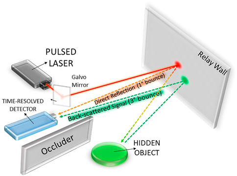
FIGURE 4. Schematic representation of NLOS set-up, with the pulsed laser (emitter) and the time-resolved SPAD detector (receiver). Both direct reflection and third bounce are visible.
Beyond applying a sharp time-filtering of incoming light, unique feature of both these devices is their temporal response of just a few tens of picoseconds: timing jitter is also an important parameter for NLOS imaging, as it ultimately limits the achievable transverse and axial resolution of the reconstruction [100], which in these cases is in the centimeter range. Leaning towards the employment of wider sensors to further speed up exposures, monolithic SPAD array architectures combining low-jitter with time-gating capabilities are required in order to effectively parallelize the acquisition. To prevent the use of bulky and expensive external units computing photon TOF on multiple channels, NLOS imaging system would also benefit from including TCSPC functionalities on-chip, by embedding multiple TDCs within the sensor itself. While several imagers providing gated-mode operation have been presented in literature, just a few employ hard gating [20, 32, 58, 101], whereas the vast majority provide only soft gating [47, 49, 102]. The latter solution does not prevent the SPADs to be blinded by bright first-bounce reflections preceding further scattered photons, the former is not typically coupled with acceptable jitter performance to comply with NLOS accuracy specifications. Given the demand for suitable imagers to prove the scalability of NLOS imaging technique, some novel NLOS tailored architectures are emerging [46]. However, none has been employed in practical measurements yet, hence they cannot be fairly compared to the state-of-the-art.
Raman Spectroscopy
Raman Spectroscopy (RS) is a technique for nondestructively investigating the chemical and molecular composition of a sample. It is based on the inelastic scattering of photons that causes minor wavelength shifts from the excitation wavelength, known as Stokes and AntiStokes shifts [103]. Raman signals are usually very weak and often overshadowed by fluorescence signals. One promising method to suppress the effect of auto-fluorescence is Time-Gated RS (TG-RS) [104], which relies on their different time responses: fluorescence emission decays with lifetimes in the nanoseconds range, whereas Raman scattering is an instantaneous phenomenon coincident with light excitation (sub-picoseconds to picoseconds time scales). The combination of short laser pulses with time-gated detectors enables the collection of only those photons synchronous with the pulse, thus rejecting fluorescent ones.
SPAD arrays are the most suitable single-photon detectors to be rapidly and precisely time-gated without bulky, complex, or expensive setups. A number of SPAD-based RS systems have emerged in the past years [105], mostly linear arrays of one or a few lines, since the diffraction element included in a typical spectrometer spreads Raman wavelengths across a spectrum of lines, as shown in Figure 5. SPADs can be easily time-gated, through SPAD frontend circuitry [8, 16, 106]. Also soft gating is employed in RS [107]. Soft gating is advantageous from the power dissipation point of view, but hard gating avoids the SPAD being blinded by a former fluorescence trigger just before the next laser pulse, especially when using a high repetition rate laser. Both counting and timing electronics have been employed in RS applications, since Raman discrimination can be performed either with SPC during short gate windows [15, 16] or with TCSPC through TDC-based arrays [21, 58, 106, 107]. TCSPC requires more complex and power demanding architectures, but it enables further possibilities, such as measuring the background fluorescence decay constant and consequently estimating the fluorescence photon counts overlapped to Raman ones. Especially in SPC, high-resolution delay lines and smart routing measures are fundamental to get all pixels activated in the same time interval, perfectly synchronized with the laser pulse, to avoid distortion in the detected Raman spectrum. On-chip delay lines typically allow better results than commercial off-chip ones in terms of stability, time resolution, and linearity [15, 106]. Conversely, when fluorescence is rejected by post-processing TDC data, the gate signals can be slower and less precise since the ultimate limit becomes the TDC linearity. However, TCSPC imposes to integrate a TDC per pixel, it lacks the possibility of storing multiple photon counts per pixel per time-frame, and it requires a longer readout. As a future trend, additional on-chip processing electronics could be included, e.g., to provide the address of pixels detecting higher intensity Raman peaks, so to speed up molecule identification, or, on the heels of fluorescence decay peak identification, on-chip histogramming [106]. Integration of high functionality and low power consumption electronics will certainly be encouraged by recent 3D-stacking progresses.
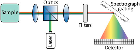
FIGURE 5. Schematic representation of Raman Spectroscopy optical system, with the pulsed laser, the spectrograph grating and the time-resolved linear SPAD detector.
Biophotonic Applications
Biophotonic applications include different imaging techniques such as Fluorescence Lifetime Imaging (FLIM), Förster Resonance Energy Transfer (FRET), Fluorescence Correlation Spectroscopy (FCS), Diffuse Correlation Spectroscopy (DCS), and Near Infrared Optical Tomography (NIROT).
FLIM is a non-invasive technique that measures the time-resolved optical properties of a fluorophore (i.e., its fluorescence lifetime), allowing to observe and quantify molecules inside a sample. The image is constructed based on the differences in the decay rate of excited states. This kind of technique is particularly powerful since the lifetime of the fluorophore depends on its molecular environment, but not on its concentration, allowing the study of molecular scale effects independently of the fluorophore concentration [108]. FLIM is achieved by two methods: point scanning and wide-field imaging. The former builds up the image one pixel at a time and exploits scanning to reconstruct the image, the latter instead uses multi-pixel detectors collecting simultaneously data from each pixel, with a clear advantage in terms of measurement time. One fundamental detector requirement is sub-nanosecond timing resolution to determine the fluorescence lifetime, and therefore both highly accurate TCSPC and gated-SPC SPADs arrays can be employed. Examples of gated-SPC arrays for FLIM are the detector described in Pancheri [14] and the planar FluoCam by Homulle [109] that reaches 12.3 ps resolution [53]. Different possibilities to fulfill this high-resolution requirement are throughout the employment of TDCs on-chip, like the ones developed by Krstajić [19] and Erdogan [22] in their linear arrays. Finally, to obtain a better flexibility, dual architectures with both gated and TCSPC SPAD arrays have been used for widefield FLIM, like the SwissSpad 512 × 128 [49] or TCSPC 64 × 64 matrix by Schwartz [36].
FRET is a process in which energy is transferred in a non-radiative way from a donor molecular fluorophore to an acceptor fluorophore, and it is generally used for various biological applications to study molecules structure, conjugated antibodies, cytochemical identification or cells metabolism. This microscopy imaging technique is applied in protein studies and relies on the ability to capture the signal from the interaction of the labeled molecules. The fluorescence signals from the donor
where
Planar [112] and linear [106, 107] arrays are used in this kind of imaging technique and both of them can usually be employed or only in TCSPC [112], or exploiting both SPC and TCSPC [106, 107]. Additional features are sometimes added, like per-pixel histogramming mode, allowing to decrease the post-processing computational weight.
FCS is a technique that measures the fluorescence intensity fluctuations, in fact, by recording temporal changes in fluorescence emission it is possible to quantify concentration, shape and size of molecules. The analysis autocorrelation function
The development of theoretical models has allowed to describe the relation between the processes causing fluorescence fluctuation and the shape of the autocorrelation function
DCS is a method to optically measure and observe microvascular blood flow, a fundamental parameter since it affects the delivery of oxygen and other nutrients to tissues. A lot of diseases are correlated with anomalous blood flow, like stroke, circulatory problems and cancer [30, 115]. The measurement of this parameter is very demanding, especially considering the need for high accuracy, stability, rapidity, and noninvasive approaches. In DCS the speckle interference pattern of a coherent near-infrared light source is measured after it has scattered within the tissue. The movement of blood cells causes a fluctuation of the pattern proportionally to the flow rate, which is estimated by computing the temporal intensity autocorrelation curve. In Tamborini [116] a time-resolved DCS technique has been proposed; through the evaluation of photon TOF the system was able to distinguish and measure blood flow at different depths. A 32 × 32 matrix by Photon Force (PF-32) has been used for DCS purposes by Liu [117]. By averaging over a thousand of independent speckle fluctuation measurements it was possible, in tissue-like phantom, to have an accurate detection of mm-scale perturbations. Finally, another system for DCS has been described in Johansson [118], where a 5 × 5 matrix with integrated readout and quenching electronics is used and tested on milk phantoms and blood occlusion in vivo experiments [97].
NIROT allows to detect oxygenation in tissues with high-spatial resolution, fundamental for hypoxia or ischemia diagnosis purposes. NIROT is constituted by a set of sources and detectors placed in different patterns: a source emits light into the tissue while detectors measure the re-emerging light. This technique is classified in three modes of illumination and acquisition: Time-resolved (TR), frequency-domain (FD) and continuous wave (CW) NIROT. In TR-NIROT the source emits short pulses while the detector measures the arrival times of the photons. The timing data provide the most complete set of information, making TR more common with respect to FD and CW. Pioneer [119] is a TR-NIROT system that employs 11 laser sources arranged in a circular pattern to generate pico-second light pulses in NIR range. The detector is a 32 × 32 SPAD matrix [45] with 128 TDC to evaluate photons TOFs, information then processed by the FPGA to build per-pixel histograms.
Quantum Imaging
SPADs in quantum field are documented since the first years of the 2000s, being present in seminal works like the first demonstrations of deterministic Single-Photon Sources [120], and are widely used in Quantum Photonics [121] and Quantum Imaging.
Quantum imaging includes those image formation processes that involve quantum states of light, which, compared to their classical counterparts, allow higher SNR measurements. The advantages can be described both in terms of sensitivity and resolution [122, 123]. In classical imaging, the maximum sensitivity is related to the mean energy of the probe light, and it is equal to
The detection of photon temporal correlation is the common ground among all quantum imaging techniques. The type of photon coincidences involved in quantum imaging usually regards only two photons with a small time difference (in the order of 500 fs), due to the coherence time of entangled photons, and potentially everywhere distributed on the detector area (with coincidence spatial information required to reconstruct a wide-field image). The first way to detect photon coincidences is by off-chip postprocessing the timing information of the integrated TDCs, whose resolution defines the coincidence time window, down to tens of picoseconds [33, 133]. If the TDCs are integrated into each SPAD pixel, spatial information at the single SPAD level is preserved, with the associated power consumption impact. The TDC-approach requires a fixed-frame rate readout of all pixels timing information, negatively impacting on exposure times, processing capability, and storage availability, given the low number of expected photons in quantum imaging measurements. A better solution is represented by an on-chip coincidence detection followed by an event-driven readout optimized to skip empty pixels/rows [32, 40] or ideally transfer only the positions of pixels detecting coincident photons, on the heels of event-driven address readout of single-pixel events [33]. The on-chip coincidence detection is hardly feasible with a fully digital approach, since counting SPADs digital outputs combined in OR/XOR/mux-tree networks causes the loss of sub-picosecond coincidences [36, 40], while detection circuits based on adders or AND-gate networks [17, 32] are only manageable within area-limited subarrays. The best options for on-chip coincidence detection are mixed analog and digital architectures, where the analog SiPM concept of current sensing is exploited, but SPADs noise immunity and spatial information are preserved [40, 51]. However, these architectures still need optimizations to become scalable in large arrays (i.e., to handle possible mismatches in signal paths and process variations across the chip area) and to achieve short coincidence time windows, currently in the order of few nanoseconds.
For a given detector area, the higher the number of pixels, the better the spatial resolution in the image formation. In-pixel electronics only constituted by low-area consuming circuitry or electronics moved aside the sensitive area are beneficial in terms of pixel density, however, a small pixel pitch increases the probability of crosstalk. Being crosstalk events temporally coincident, they result in false coincident events that can completely hide useful information. For this reason, crosstalk should be minimized during the detector design phase and characterized after production to implement postprocessing algorithms to mitigate its effects [134]. Signal correlations can also be hidden by accidental coincidences due to single photons being detected simultaneously: the longer the coincidence time window, the higher the probability of false coincidences [135]. Spurious detections result from dark count events or photon losses in the optical path (due to source, optics or detector inefficiencies). The effect of dark counts can be mitigated by disabling noisy pixels [36, 44, 51]. Optical losses can be minimized by optimizing PDP and FF of the detector. Differential imaging protocols, profiting from entangled states, bring new flexibility to the spectral ranges at which the properties of objects can be measured (e.g., illuminating wavelengths different from detected wavelengths), thus it becomes easier to match the detector peak efficiency [136]. Considering the needs for high FF and low crosstalk probability, despite the increase in costs and complexity, a trade-off solution is represented by MLAs. MLAs usually present optimal performance for high f-numbers, a requirement typically fulfilled in quantum imaging set-ups where collimated light beams are employed.
Radiation Detection
SPAD arrays can be used as radiation detectors, combined with scintillators able to absorb high-energy radiation and convert it into a pulse of visible photons, above all in PET applications. PET is a nuclear medicine imaging technique that exploits radiotracers to visualize and measure changes in metabolic processes and in other physiological activities [137]. It is employed in fields such as neuroimaging, cardiology, and oncology. A positron emitter is inserted in the patient: after a positron is emitted within the patient body, it travels for a distance of about 1 mm in the tissue before colliding with a free electron and annihilating. The result of annihilation is the generation of a pair of 511 keV gamma photons moving toward opposite directions. PET splits the detection process into two phases. As first step, the incoming gamma rays are absorbed by a scintillation material, i.e., a material that is able to emit visible photon in response to the absorption of higher energy radiation. The produced visible photons are then detected with SPDs for visible light, such as Photomultiplier Tubes (PMT) or SiPMs [138, 139, 140]. By making statistical fluctuations negligible, through a sufficiently high number of acquisitions, it is possible to locate the source of these photons along the axis of emission, so that the position of the radioactive tracer in the patient’s body can be reconstructed (see Figure 6). In fact, conventional PET is able to define the line along which the interaction has taken place by identifying the couple of detectors firing at the same time. However, it is possible to improve the spatial resolution by measuring also the TOF of the detected γ-rays. By adding this data, the position of the interaction along the line can be precisely measured, so to achieve better spatial resolution for a given radiation dose, or to reduce either dose or total acquisition time for the same image resolution.
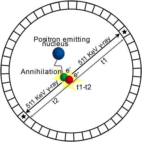
FIGURE 6. Schematic representation of a TOF-PET scanner.
The push toward SPAD arrays and SiPMs exploitation as visible light detectors in this application started in the years 2000 for PET/MRI multimodality requiring magnetic field immunity, not ensured by PMTs [141]. To efficiently couple the emission of the scintillator, essential requirements are large active area (some mm2) and high FF. While analog-SiPMs are undoubtedly competitive for their large gain, SPAD arrays and digital-SiPMs can offer on-chip data processing and timestamping capability. Given the digital SPAD output independent of the number of impinging photons, SPAD pixels density in arrays should be adequate to avoid saturation effects for the incoming light flux. With high SPAD densities, crosstalk reduction measures should always be taken into account. The employed photodetector must ensure photon number resolving capability so to discard low-energy light (giving few photons per scintillation burst) coming from background Compton scattering events, and single-photon time resolution in the order of 100 ps. FBK NUV-HD SiPM, with 40 μm SPAD pitch and 4 × 4 mm2 device area, has measured time resolution values of 70 ps [142]. TOF performance sets requirements on the employed TDCs (e.g., precision, range, linearity) and overall system jitter. Moreover, for high-performance full-body TOF-PET, timing performance must be traded-off with power consumption (which increases proportionally to the required electronic bandwidth), system integration, and cost.
Beyond visible spectrum, research showed the capability of SPADs to detect accelerated electrons in the energy from 5 to 30 keV, which passing through the detector transfer electron flux to the electrons in the depleted region via inelastic scattering, generating carriers (impact ionization) that ultimately cause avalanche breakdown [143]. In addition, experiments have been investigating SPAD detection of X-rays with 3D-stacked BSI SPAD image sensor for SPC and time-resolved imaging [144]. The reported X-ray irradiator generates X-rays with peak photon energies from 30 to 120 keV, which cause proportional average per pixel counts, with no permanent damage or increase in dark count events after exposure [143].
Discussion
As shown in the paper, in the last decades, SPAD arrays have emerged as the most suitable photodetectors for both SPC and TCSPC applications. After the implementation of the first SPADs in standard CMOS technology, research has focused on the design of large digital SPAD imagers assembled in integrated SPAD arrays. Also the frontend and processing electronics followed such path, moving from off-chip data post-elaboration to progressively “smarter” sensors including on-chip timestamping and processing capabilities (e.g., also including a DSP in the same sensor chip [72]). The choice of different pixel and array geometry and configurations, and of the integrated features is strongly bounded to the target application. For instance, linear arrays are more indicated for spectrographic applications, whereas 2D arrays are better fits for high frame rate imaging. Generally speaking, developing larger arrays allows a parallelization of the acquisition, reducing the measurement time. However, SPAD arrays still present relatively large pixel pitch (down to 6 μm in the best case [74]) and higher power consumption with respect to conventional image sensors. On the other hand, operating in Geiger mode, they provide single photosensitivity. When compared with other single-photon detectors (such as PMTs or Superconductive Nanowire Single-Photon Detectors—SNSPDs), they present spatial resolution coupled to sub-nanosecond temporal resolution (needed in all the applications based on TCSPC), room temperature operation and ruggedness, at the expense of a limited PDE in respect to SNSPDs. Moreover, they offer the possibility of rapidly (in few hundreds ps) enabling or disabling the sensors, an essential feature in those applications where a strong first laser reflection would saturate the SPAD and prevent the measurement of the late photons carrying the useful information, as for example happens in NLOS [100] and NIROT [119].
Beyond research applications, in which SPADs have been used for several decades, SPADs are recently gaining interest also for commercial exploitation in industrial, automotive, and consumer electronics fields, pushing many big Silicon companies (such as STMicroelectronics, Sony, Samsung, and Canon) to develop SPAD arrays. In particular, a fast-growing interest has been placed lately in LiDAR for automotive, where high-sensitive, time-resolved, and reliable sensors are required for autonomously driven cars [145]. Arrays designed for research purposes often have performance limited by the technology and the production costs, while the involvement of major companies helps in pushing beyond these limits by employing technologies, such as 3D stacking, that allow optimum performance for both detectors and electronics [72, 75]. The development of specific microlens arrays for SPAD imagers, also allows to increase the effective FF, which natively is far below the one of CCDs [11]. In this way, SPAD imagers are becoming more and more competitive with other more established imaging technologies (i.e., CCDs, Intensified-CCDs, Electron-Multiplying-CCDS, and CMOS APSs).
Various applications, among which LiDAR and quantum communication, require high PDE especially in the near-infrared range [146], characteristic in which CMOS silicon SPADs are still lacking. Despite the progress in CMOS SPAD performance (especially in BSI technologies), custom technologies still present higher sensitivity to red and NIR lights and wider active area. On the other hand, CMOS SPADs are indispensable when the application requires a detector array, as it happens, for example, in classical or quantum imaging systems.
The intrinsic deadtime, which limits the SPAD maximum count rate and so the dynamic range, is one of the drawbacks of SPADs with respect to linear detectors. Indeed, the exploitation of SPADs is limited in applications that require high detection rates such as quantum cryptography and computing, and single-photon imaging. However, many groups are currently working on optimizing also this performance, and deadtimes as low as 1 ns with negligible afterpulsing have been achieved [147].
Conclusion
The present paper is a comprehensive review about single SPAD and SPAD arrays. In particular, this Part II offers an overview of the main typologies of SPAD and SiPM arrays and their historical development with a strong focus on their on-field applications. From this, it emerges the strong importance of these devices in both SPC and TCSPC applications in many fields, such as LiDAR, NLOS, Biophotonics and Spectroscopy, quantum imaging, and radiation detection. Emerging technologies based on 3D stacking are opening the way to a new generation of SPAD detectors with short deadtime, small pixel pitch, high-pixel number, and capability to integrate on-chip image processing, which historically has been the parameters that mostly limited SPAD array applicability compared to CCDs and CMOS APSs.
Author Contributions
IC literature review, writing, review and editing of the full paper. DB, EC, AI, FM, AM, CN, SR writing of a section of the paper. FV paper organization, literature review and review of the full paper.
Conflict of Interest
The authors declare that the research was conducted in the absence of any commercial or financial relationships that could be construed as a potential conflict of interest.
Publisher’s Note
All claims expressed in this article are solely those of the authors and do not necessarily represent those of their affiliated organizations, or those of the publisher, the editors and the reviewers. Any product that may be evaluated in this article, or claim that may be made by its manufacturer, is not guaranteed or endorsed by the publisher.
References
1. Zappa F, Tisa S, Tosi A, Cova S. Principles and Features of Single-Photon Avalanche Diode Arrays. Sensors Actuators A: Phys (2007) 140:103–12. doi:10.1016/j.sna.2007.06.021
2. Bronzi D, Villa F, Tisa S, Tosi A, Zappa F. 100 000 Frames/s 64 × 32 Single-Photon Detector Array for 2-D Imaging and 3-D Ranging. IEEE J Selected Top Quan Electron (2014) 20(6):355–64. doi:10.1109/jstqe.2014.2341562
3. Dalla Mora A, Tosi A, Zappa F, Cova S, Contini D, Pifferi A, et al. Fast-gated Single-Photon Avalanche Diode for Wide Dynamic Range Near Infrared Spectroscopy. IEEE J Select Top Quan Electron. (2010) 16(4):1023–30. doi:10.1109/jstqe.2009.2035823
4. Renna M, Nam JH, Buttafava M, Villa F, Velten A, Tosi A. Fast-Gated 16×1 SPAD Array for Non-line-of-sight Imaging Applications. Instruments (2020) 414(2). doi:10.3390/instruments4020014
5. Musarra G, Lyons A, Conca E, Altmann Y, Villa F, Zappa F, et al. Non-Line-of-sight Three-Dimensional Imaging with a Single-Pixel Camera. Phys Rev Appl (2019) 12(1). doi:10.1103/physrevapplied.12.011002
6. Yang H, Luo G, Karnchanaphanurach P, Louie T-M, Rech I, Cova S, et al. Protein Conformational Dynamics Probed by Single-Molecule Electron Transfer. Science (2003) 302(5643):262–6. doi:10.1126/science.1086911
7. Zappa F, Ghioni M, Cova S, Varisco L, Sinnis B, Morrison A, et al. Integrated Array of Avalanche Photodiodes for Single-Photon Counting. In: Proc. Eur. Solid-State Device Research Conf. ESSDERC (1997). p. 22–4.
8. Rochas A, Gosch M, Serov A, Besse PA, Popovic RS, Lasser T, et al. First Fully Integrated 2-D Array of Single-Photon Detectors in Standard CMOS Technology. IEEE Photon Technol Lett (2003) 15(7):963–5. doi:10.1109/lpt.2003.813387
9. Conca E, Cusini I, Severini F, Lussana R, Zappa F, Villa F. Gated SPAD Arrays for Single-Photon Time-Resolved Imaging and Spectroscopy. IEEE Photon J. (2019) 11(6):1–10. doi:10.1109/jphot.2019.2952670
10. Dilhan L, Vaillant J, Ostrovsky A, Masarotto L, Pichard C, Paquet R. Planar Microlenses for Near Infrared CMOS Image Sensors. Electron Imaging (2020) 32(7). doi:10.2352/issn.2470-1173.2020.7.iss-144
11. Intermite G, McCarthy A, Warburton RE, Ren X, Villa F, Lussana R, et al. Fill-factor Improvement of SI CMOS Single-Photon Avalanche Diode Detector Arrays by Integration of Diffractive Microlens Arrays. Opt Express (2015) 23(26):33777. doi:10.1364/oe.23.033777
12. Niclass C, Sergio M, Charbon E. A Single Photon Avalanche Diode Array Fabricated in Deep-Submicron CMOS Technology. In: Proceedings of the Design Automation & Test in Europe Conference (2006). p. 1–6. doi:10.1109/date.2006.243987
13. Sergio M, Niclass C, Charbon E. A 128×2 CMOS Single-Photon Streak Camera with Timing-Preserving Latchless Pipeline Readout. In: 2007 IEEE International Solid-State Circuits Conference (2007). p. 394–610. Digest of Technical Papers.
14. Pancheri L, Stoppa D. A SPAD-Based Pixel Linear Array for High-Speed Time-Gated Fluorescence Lifetime Imaging. In: 2009 Proceedings of ESSCIRC (2009). p. 428–31. doi:10.1109/esscirc.2009.5325948
15. Maruyama Y, Blacksberg J, Charbon E. A 1024$\,\times\,$8, 700-ps Time-Gated SPAD Line Sensor for Planetary Surface Exploration with Laser Raman Spectroscopy and LIBS. IEEE J Solid-state Circuits (2014) 49(1):179–89. doi:10.1109/jssc.2013.2282091
16. Nissinen I, Nissinen J, Keranen P, Lansman A-K, Holma J, Kostamovaara J. A $2\times (4)\times 128$ Multitime-Gated SPAD Line Detector for Pulsed Raman Spectroscopy. IEEE Sensors J (2015) 15(3):1358–65. doi:10.1109/jsen.2014.2361610
17. Niclass C, Soga M, Matsubara H, Kato S, Kagami M. A 100-m Range 10-Frame/s 340$\,\times\, $96-Pixel Time-Of-Flight Depth Sensor in 0.18-$\mu\hbox{m}$ CMOS. IEEE J Solid-state Circuits (2013) 48(2):559–72. doi:10.1109/jssc.2012.2227607
18. Villa F, Lussana R, Tamborini D, Tosi A, Zappa F. High-Fill-Factor $60\times 1$ SPAD Array with 60 Subnanosecond Integrated TDCs. IEEE Photon Technol Lett (2015) 27(12):1261–4. doi:10.1109/lpt.2015.2416192
19. Krstajić N, Levitt J, Poland S, Ameer-Beg S, Henderson R. 256 × 2 SPAD Line Sensor for Time Resolved Fluorescence Spectroscopy. Opt Express (2015) 23:5653–69. doi:10.1364/OE.23.005653
20. Nissinen I, Nissinen J, Holma J, Kostamovaara J. A 4 × 128 SPAD Array with a 78-ps 512-channel TDC for Time-Gated Pulsed Raman Spectroscopy. Analog Integr Circ Sig Process (2015) 84:353–62. doi:10.1007/s10470-015-0592-1
21. Nissinen I, Nissinen J, Keranen P, Stoppa D, Kostamovaara J. A $16\times256$ SPAD Line Detector with a 50-ps, 3-bit, 256-Channel Time-To-Digital Converter for Raman Spectroscopy. IEEE Sensors J (2018) 18(9):3789–98. doi:10.1109/jsen.2018.2813531
22. Erdogan AT, Walker R, Finlayson N, Krstajic N, Williams GOS, Henderson RK. A 16.5 Giga Events/s 1024 × 8 SPAD Line Sensor with Per-Pixel Zoomable 50ps-6.4ns/bin Histogramming TDC. In: 2017 Symposium on VLSI Circuits (2017). p. C292–C293.
23. Erdogan AT, Walker R, Finlayson N, Krstajic N, Williams G, Girkin J, et al. A CMOS SPAD Line Sensor with Per-Pixel Histogramming TDC for Time-Resolved Multispectral Imaging. IEEE J Solid-state Circuits (2019) 54(6):1705–19. doi:10.1109/jssc.2019.2894355
24. Yoon HSH, Kim D, Kim J, Kim SJ, Chun JH, Choi J. A 36-Channel SPAD-Integrated Scanning LiDAR Sensor with Multi-Event Histogramming TDC and Embedded Interference Filter. In: 2020 IEEE Symposium on VLSI Circuits (2020). p. 1–2.
25. Burri S, Bruschini C, Charbon E. LinoSPAD: A Compact Linear SPAD Camera System with 64 FPGA-Based TDC Modules for Versatile 50 Ps Resolution Time-Resolved Imaging. Instruments (2017) 1(1):6. doi:10.3390/instruments1010006
26. Cuccato A, Antonioli S, Crotti M, Labanca I, Gulinatti A, Rech I, et al. Complete and Compact 32-channel System for Time-Correlated Single-Photon Counting Measurements. IEEE Photon J. (2013) 5(5):6801514. doi:10.1109/jphot.2013.2284250
27. Incoronato A, Severini F, Villa F, Zappa F. Multi-Channel SPAD Chip for Silicon Photonics with Multi-Photon CoIncidence Detection. IEEE J Select Top Quan Electron. (2022) 28(3):1–7. doi:10.1109/jstqe.2021.3134071
28. Maruyama Y, Charbon E. An All-Digital, Time-Gated 128 × 128 SPAD Array for On-Chip, Filter-Less Fluorescence Detection. In: Solid-State Sensors Actuators and Microsystems Conference (2011). p. 1180–3.
29. Henderson RK, Johnston N, Mattioli Della Rocca F, Chen H, Day-Uei Li D, Hungerford G, et al. A $192\times128$ Time Correlated SPAD Image Sensor in 40-nm CMOS Technology. IEEE J Solid-state Circuits (2019) 54(7):1907–16. doi:10.1109/jssc.2019.2905163
30. Serov MGA, Rochas A, Blom H, Anhut T, Besse P-A, Popovic R, et al. Parallel Single Molecule Detection with a Fully Integrated Single-Photon 2×2 CMOS Detector Array. J Biomed Opt (2004) 9(5):913.
31. Buttafava M, Villa F, Castello M, Tortarolo G, Conca E. SPAD-based Asynchronous-Readout Array Detectors for Image-Scanning Microscopy. Optica (2020). doi:10.1364/optica.391726
32. Berkovich A, Datta T, Abshire P. A Scalable 20×20 Fully Asynchronous SPAD-Based Imaging Sensor with AER Readout. In: Proceedings of the IEEE International Symposium on Circuits and Systems (ISCAS); Lisbon, Portugal (2015). p. 1110–3.
33. Niclass C, Sergio M, Charbon E. A CMOS 64×48 Single Photon Avalanche Diode Array with Event-Driven Readout. In: Proceedings of the 32nd European Solid-State Circuits Conference (ESSCIRC); Montreux, Switzerland (2006). p. 556–9. doi:10.1109/esscir.2006.307485
34. Portaluppi D, Conca E, Villa F. 32 × 32 CMOS SPAD Imager for Gated Imaging, Photon Timing, and Photon Coincidence. IEEE J Select Top Quan Electron. (2018) 24(2):1–6. doi:10.1109/jstqe.2017.2754587
35. Gersbach M, Maruyama Y, Trimananda R, Fishburn MW, Stoppa D, Richardson JA, et al. A Time-Resolved, Low-Noise Single-Photon Image Sensor Fabricated in Deep-Submicron CMOS Technology. IEEE J Solid-state Circuits (2012) 47(6):1394–407. doi:10.1109/jssc.2012.2188466
36. Braga LHC, Gasparini L, Grant L, Henderson RK, Massari N, Perenzoni M, et al. A Fully Digital 8$\,\times\,$16 SiPM Array for PET Applications with Per-Pixel TDCs and Real-Time Energy Output. IEEE J Solid-state Circuits (2014) 49:301–14. doi:10.1109/jssc.2013.2284351
37. Schwartz DE, Charbon E, Shepard KL. A Single-Photon Avalanche Diode Array for Fluorescence Lifetime Imaging Microscopy. IEEE J Solid-state Circuits (2008) 43(11):2546–57. doi:10.1109/jssc.2008.2005818
38. Richardson J, Walker R, Grant L, Stoppa D, Borghetti F. A 32×32 50ps Resolution 10 Bit Time to Digital Converter Array in 130nm CMOS for Time Correlated Imaging. In: 2009 IEEE Custom Integrated Circuits Conference (2009). p. 77–80.
39. Villa F, Lussana R, Bronzi D, Tisa S, Tosi A, Zappa F, et al. CMOS Imager with 1024 SPADs and TDCs for Single-Photon Timing and 3-D Time-Of-Flight. IEEE J Select Top Quan Electron. (2014) 20(6):364–73. doi:10.1109/jstqe.2014.2342197
40. Manuzzato E, Gioscio E, Mattei I, Mirabelli R, Patera V, Sarti A, et al. A $16\times8$ Digital-SiPM Array with Distributed Trigger Generator for Low SNR Particle Tracking. In: ESSCIRC 2019 - IEEE 45th European Solid State Circuits Conference (ESSCIRC), 2 (2019). p. 75–8. doi:10.1109/lssc.2019.2934598IEEE Solid-state Circuits Lett
41. Perenzoni M, Massari N, Perenzoni D, Gasparini L, Stoppa D. A 160×120-pixel Analog-Counting Single-Photon Imager with Sub-ns Time-Gating and Self-Referenced Column-Parallel a/D Conversion for Fluorescence Lifetime Imaging. In: 2015 IEEE International Solid-State Circuits Conference - (ISSCC) (2015). Digest of Technical Papers.
42. Niclass C, Favi C, Kluter T, Gersbach M, Charbon E. A 128 $\times$ 128 Single-Photon Image Sensor with Column-Level 10-Bit Time-To-Digital Converter Array. IEEE J Solid-state Circuits (2008) 43(12):2977–89. doi:10.1109/jssc.2008.2006445
43. Braga LH, Pancheri L, Gasparini L, Perenzoni M, Walker R. A CMOS Mini-SiPM Detector with In-Pixel Data Compression for PET Applications. In: 2011 IEEE Nuclear Science Symposium Conference Record (2011). p. 548–52. doi:10.1109/nssmic.2011.6154110
44. Carimatto A, Ulku A, Lindner S, D'Aillon E, Rae B. Multipurpose, Fully-Integrated 128×128 Event-Driven MD-SiPM with 512 16-Bit TDCs with 45 PS LSB and 20 NS Gating. In: 2018 IEEE Symposium on VLSI Circuits (2018). p. 73–4.
45. Zhang C, Lindner S, Antolovic I, Wolf M, Charbon E. A CMOS SPAD Imager with Collision Detection and 128 Dynamically Reallocating TDCs for Single-Photon Counting and 3d Time-Of-Flight Imaging. Sensors (2018) 18(11):4016. doi:10.3390/s18114016
46. Riccardo S, Conca E, Sesta V, Tosi A. Fast-gated 16×16 SPAD Array with On-Chip 6 PS Tdcs for Non-line-of-sight Imaging. In: 2021 IEEE Photonics Conference (IPC) (2021).
47. Jahromi S, Jansson J-P, Keranen P, Kostamovaara J. A 32 × 128 SPAD-257 TDC Receiver IC for Pulsed TOF Solid-State 3-D Imaging. IEEE J Solid-state Circuits (2020) 55(7):1960–70. doi:10.1109/jssc.2020.2970704
48. Parmesan L, Dutton NAW, Clader NJ, Krastajic N, Holmes AJ. A 256×256 SPAD Array with In-Pixel Time to Amplitude Conversion for Fluorescence Lifetime Amplitude Conversion for Fluorescence Lifetime Imaging Microscopy. In: Proceeding International Image Sensor Workshop (2015). p. M5.
49. Perenzoni M, Perenzoni D, Stoppa D. A 64 × 64-Pixels Digital Silicon Photomultiplier Direct TOF Sensor with 100-MPhotons/s/pixel Background Rejection and Imaging/Altimeter Mode with 0.14% Precision up to 6 Km for Spacecraft Navigation and Landing. IEEE J Solid-State Circuits (2017) 52(1):151–60.
50. Conca E, Sesta V, Buttafava M, Villa F, Sieno LD, Mora AD, et al. Large-Area, Fast-Gated Digital SiPM with Integrated TDC for Portable and Wearable Time-Domain NIRS. IEEE J Solid-state Circuits (2020) 55(11):3097–111. doi:10.1109/jssc.2020.3006442
51. Gasparini L, Zarghami M, Xu H, Parmesan L, Garcia MM, Unternahrer M, et al. A 32×32-pixel Time-Resolved Single-Photon Image Sensor with 44.64 μm Pitch and 19.48% Fill-Factor with On-Chip Row/frame Skipping Features Reaching 800 kHz Observation Rate for Quantum Physics Applications. In: Proceedings of the IEEE International Solid-State Circuits Conference (ISSCC); San Francisco, CA, USA (2018). p. 98–100.
52. Burri S, Maruyama Y, Michalet X, Regazzoni F, Bruschini C, Charbon E. Architecture and Applications of a High Resolution Gated SPAD Image Sensor. Opt Express (2014) 22(14):17573. doi:10.1364/oe.22.017573
53. Niclass C, Favi C, Kluter T, Monnier F, Charbon E. Single-Photon Synchronous Detection. IEEE J Solid-state Circuits (2009) 44(7):1977–89. doi:10.1109/jssc.2009.2021920
54. Lee C, Johnson B, Jung T, Molnar A. A 72 × 60 Angle-Sensitive SPAD Imaging Array for Lens-Less FLIM. Sensors (Basel) (2016) 16(9). doi:10.3390/s16091422
55. Kim B, Park S, Chun J-H, Choi J, Kim S-J. A 48×40 13.5mm Depth Resolution Flash Lidar Sensor with In-Pixel Zoom Histogramming Time-To-Digital Converter. In: 2021 IEEE International Solid- State Circuits Conference (ISSCC) (2021).
56. Seo H, Yoon H, Kim D, Kim J, Kim S-J, Chun J-H, et al. Direct TOF Scanning Lidar Sensor with Two-step Multievent Histogramming TDC and Embedded Interference Filter. IEEE J Solid-state Circuits (2021) 56(4):1022–35. doi:10.1109/jssc.2020.3048074
57. Zhang C, Lindner S, Antolovic IM, Mata Pavia J, Wolf M, Charbon E. A 30-frames/s, $252\times144$ SPAD Flash LiDAR with 1728 Dual-Clock 48.8-ps TDCs, and Pixel-Wise Integrated Histogramming. IEEE J Solid-state Circuits (2019) 54(4):1137–51. doi:10.1109/jssc.2018.2883720
58. Ulku AC, Bruschini C, Antolovic IM, Kuo Y, Ankri R, Weiss S, et al. A 512 × 512 SPAD Image Sensor with Integrated Gating for Widefield FLIM. IEEE J Select Top Quan Electron. (2019) 25(1):1–12. doi:10.1109/jstqe.2018.2867439
59. Morimoto K, Ardelean A, Wu M-L, Ulku AC, Antolovic IM, Bruschini C, et al. Megapixel Time-Gated SPAD Image Sensor for 2D and 3D Imaging Applications. Optica (2020) 7(4). doi:10.1364/optica.386574
60. Iwabuchi S, Maruyama Y, Ohgishi Y, Muramatsu M, Karasawa N, Hirayama T. A Back-Illuminated High-Sensitivity Small-Pixel Color CMOS Image Sensor with Flexible Layout of Metal Wiring. In: 2006 IEEE International Solid State Circuits Conference (2006). p. 1171–8. Digest of Technical Papers. doi:10.1109/isscc.2006.1696162
61. Beyne E. The 3-D Interconnect Technology Landscape. IEEE Des Test (2016) 33(3):8–20. doi:10.1109/mdat.2016.2544837
62. Hu H-W, Chen K-N. Development of Low Temperature Cu Cu Bonding and Hybrid Bonding for Three-Dimensional Integrated Circuits (3D IC). Microelectronics Reliability (2021) 127:114412. doi:10.1016/j.microrel.2021.114412
63. Wang L, Fountain G, Lee B, Gao G, Uzoh C, McGrath S, et al. Direct Bond Interconnect (DBI®) for fine-pitch Bonding in 3D and 2.5D Integrated Circuits. In: 2017 Pan Pacific Microelectronics Symposium (Pan Pacific) (2017). p. 1–6.
64. Aull B, Burns J, Chen C, Felton B, Hanson H, Keast C, et al. Laser Radar Imager Based on 3D Integration of Geiger-Mode Avalanche Photodiodes with Two SOI Timing Circuit Layers. In: 2006 IEEE International Solid State Circuits Conference (2006). p. 1179–88. Digest of Technical Papers. doi:10.1109/isscc.2006.1696163
65. Pavia JM, Scandini M, Lindner S, Wolf M, Charbon E. A 1 × 400 Backside-Illuminated SPAD Sensor with 49.7 Ps Resolution, 30 pJ/Sample TDCs Fabricated in 3D CMOS Technology for Near-Infrared Optical Tomography. IEEE J Solid-state Circuits (2015) 50(10):2406–18. doi:10.1109/jssc.2015.2467170
66. Al Abbas T, Almer O, Hutchings SW, Erdogan AT, Gyongy I, Dutton NAW, et al. A 128×120 5-wire 1.96mm2 40nm/90nm 3D Stacked SPAD Time Resolved Image Sensor SOC for Microendoscopy. In: 2019 Symposium on VLSI Circuits (2019).
67. Hutchings SW, Johnston N, Gyongy I, Al Abbas T, Dutton NAW, Tyler M, et al. A Reconfigurable 3-D-Stacked SPAD Imager with In-Pixel Histogramming for Flash LIDAR or High-Speed Time-Of-Flight Imaging. IEEE J Solid-state Circuits (2019) 54(11):2947–56. doi:10.1109/jssc.2019.2939083
68. Zhang C, Zhang N, Ma Z, Wang L, Qin Y, Jia J, et al. A 240 X 160 3D Stacked SPAD Dtof Image Sensor with Rolling Shutter and in Pixel Histogram for mobile Devices. IEEE Open J Solid-State Circuits Soc (2021) 2:3.
69. Ronchini Ximenes A, Padmanabhan P, Lee M-J, Yamashita Y, Yaung D-N, Charbon E. A Modular, Direct Time-Of-Flight Depth Sensor in 45/65-nm 3-D-Stacked CMOS Technology. IEEE J Solid-state Circuits (2019) 54(11):3203–14. doi:10.1109/jssc.2019.2938412
70. Padmanabhan P, Zhang C, Cazzaniga M, Efe B, Ximenes AR. A 256×128 3D-Stacked (45nm) SPAD FLASH LiDAR with 7-Level Coincidence Detection and Progressive Gating for 100m Range and 10klux Background Light. In: Proceedings of the 2021 IEEE International Solid- State Circuits Conference (ISSCC); San Francisco, CA, USA (2021). p. 111–3.
71. Gramuglia F, Muntean A, Venialgo E, Lee M-J, Lindner S, Motoyoshi M, et al. CMOS 3D-Stacked FSI Multi-Channel Digital SIPM for Time-Of-Flight Pet Applications. In: 2020 IEEE Nuclear Science Symposium and Medical Imaging Conference (NSS/MIC) (2020). doi:10.1109/nss/mic42677.2020.9507833
72. Kumagai O, Ohmachi J, Matsumura M, Yagi S, Tayu K. A 189×600 Back-Illuminated Stacked SPAD Direct Time-Of-Flight Depth Sensor for Automotive LiDAR Systems. In: 2021 IEEE International Solid- State Circuits Conference (ISSCC) (2021). p. 110–2.
73. Ogi J, Takatsuka T, Hizu K, Inaoka Y, Zhu H, Tochigi Y, et al. A 124-dB Dynamic-Range SPAD Photon-Counting Image Sensor Using Subframe Sampling and Extrapolating Photon Count. IEEE J Solid-state Circuits (2021) 56(11):3220–7. doi:10.1109/jssc.2021.3114620
74. Shimada S, Otake Y, Yoshida S, Endo S, Nakamura R, Tsugawa H, et al. A Back Illuminated 6 μm SPAD Pixel Array with High PDE and Timing Jitter Performance. In: 2021 IEEE International Electron Devices Meeting (IEDM) (2021). doi:10.1109/iedm19574.2021.9720639
75. Morimoto K, Iwata J, Shinohara M, Sekine H, Abdelghafar A, Tsuchiya H, et al. 3.2 Megapixel 3D-Stacked Charge Focusing SPAD for Low-Light Imaging and Depth Sensing. In: 2021 IEEE International Electron Devices Meeting (IEDM) (2021).
76. Niclass C, Rochas A, Besse P-A, Charbon E. Toward a 3-D Camera Based on Single Photon Avalanche Diodes. IEEE J Select Top Quan Electron. (2004) 10(4):796–802. doi:10.1109/jstqe.2004.833886
77. Niclass C, Rochas A, Besse P-A, Charbon E, Charbon E. Design and Characterization of a CMOS 3-D Image Sensor Based on Single Photon Avalanche Diodes. IEEE J Solid-state Circuits (2005) 40(9):1847–54. doi:10.1109/jssc.2005.848173
78. Raj T, Hashim FH, Huddin AB, Ibrahim MF, Hussain A. A Survey on LiDAR Scanning Mechanisms. Electronics (2020) 9(5):741. doi:10.3390/electronics9050741
79. Lussana R, Villa F, Mora AD, Contini D, Tosi A, Zappa F. Enhanced Single-Photon Time-Of-Flight 3D Ranging. Opt Express (2015) 23:24962–73. doi:10.1364/oe.23.024962
80. Niclass C, Soga M, Matsubara H, Ogawa M, Kagami M. A 0.18-$\mu$m CMOS SoC for a 100-M-Range 10-Frame/s 200$\,\times\,$96-Pixel Time-Of-Flight Depth Sensor. IEEE J Solid-state Circuits (2014) 49(1):315–30. doi:10.1109/jssc.2013.2284352
81. Gupta A, Ingle A, Gupta M. Asynchronous Single-Photon 3D Imaging. In: Proceedings of the IEEE/CVF International Conference on Computer Vision (ICCV); Seoul, Korea (2019). p. 7909–18. doi:10.1109/iccv.2019.00800
82. Buttgen B, Seitz P. Robust Optical Time-Of-Flight Range Imaging Based on Smart Pixel Structures. IEEE Trans Circuits Syst (2008) 55(6):1512–25. doi:10.1109/tcsi.2008.916679
83. Incoronato A, Locatelli M, Zappa F. Statistical Modelling of SPADs for Time-Of-Flight LiDAR. Sensors (2021) 21(13):4481. doi:10.3390/s21134481
84. Beer M, Haase J, Ruskowski J, Kokozinski R. Background Light Rejection in SPAD-Based LiDAR Sensors by Adaptive Photon Coincidence Detection. Sensors (2018) 18(12):4338. doi:10.3390/s18124338
85. You Z, Parmesan L, Pellegrini S, Henderson RK. 3µm Pitch, 1µm Active Diameter SPAD Arrays in 130 Nm CMOS Imaging Technology. In: Proceedings of the International Image Sensors Society (IISS) Workshop; Hiroshima, Japan (2017).
86. Henderson RK, Webster EAG, Walker R, Richardson JA, Grant LA. A 3 × 3, 5 Μm Pitch, 3-transistor Single Photon Avalanche Diode Array with Integrated 11 V Bias Generation in 90 Nm CMOS Technology. In: Proceedings of the IEEE Int. Electron Devices Meeting; San Francisco, CA, USA (2010). p. 336–9.
87. Morimoto K, Charbon E. High Fill-Factor Miniaturized SPAD Arrays with a Guard-Ring-Sharing Technique. Opt Express (2020) 28:13068–80. doi:10.1364/oe.389216
88. Sume A, Gustafsson M, Herberthson M, Janis A, Nilsson S, Rahm J, et al. Radar Detection of Moving Targets behind Corners. IEEE Trans Geosci Remote Sensing (2011) 49(6):2259–67. doi:10.1109/tgrs.2010.2096471
89. Lindell DB, Wetzstein G, Koltun V. Acoustic Non-line-of-sight Imaging. In: 2019 IEEE/CVF Conference on Computer Vision and Pattern Recognition (CVPR) (2019). doi:10.1109/cvpr.2019.00694
90. Katz O, Heidmann P, Fink M, Gigan S. Non-invasive Single-Shot Imaging through Scattering Layers and Around Corners via Speckle Correlations. Nat Photon (2014) 8(10):784–90. doi:10.1038/nphoton.2014.189
91. Bertolotti J, van Putten EG, Blum C, Lagendijk A, Vos WL, Mosk AP. Non-invasive Imaging through Opaque Scattering Layers. Nature (2012) 491(7423):232–4. doi:10.1038/nature11578
92. Maeda T, Wang Y, Raskar R, Kadambi A. Thermal Non-line-of-sight Imaging. In: 2019 IEEE International Conference on Computational Photography (ICCP) (2019). doi:10.1109/iccphot.2019.8747343
93. Boger-Lombard J, Katz O. Passive Optical Time-Of-Flight for Non Line-Of-Sight Localization. Nat Commun (2019) 10(1):3343. doi:10.1038/s41467-019-11279-6
94. O’Toole M, Lindell DB, Wetzstein G. Confocal Non-line-of-sight Imaging Based on the Light-Cone Transform. Nature (2018) 555(7696):338–41.
95. Lindell DB, Wetzstein G, O'Toole M. Wave-based Non-line-of-sight Imaging Using Fast F-K Migration. ACM Trans Graph (2019) 38(4):1–13. doi:10.1145/3306346.3322937
96. Liu X, Guillén I, La Manna M, Nam JH, Reza SA, Huu Le T, et al. Non-line-of-sight Imaging Using Phasor-Field Virtual Wave Optics. Nature (2019) 572(7771):620–3. doi:10.1038/s41586-019-1461-3
97. Buttafava M, Zeman J, Tosi A, Eliceiri K, Velten A. Non-line-of-sight Imaging Using a Time-Gated Single Photon Avalanche Diode. Opt Express (2015) 23(16):20997–1011. doi:10.1364/OE.23.020997
98. Nam JH, Brandt E, Bauer S, Liu X, Renna M, Tosi A, et al. Low-latency Time-Of-Flight Non-line-of-sight Imaging at 5 Frames Per Second. Nat Commun (2021) 12(1). doi:10.1038/s41467-021-26721-x
99. Buttafava M, Boso G, Ruggeri A, Dalla Mora A, Tosi A. Time-gated Single-Photon Detection Module with 110 Ps Transition Time and up to 80 MHz Repetition Rate. Rev Scientific Instr (2014) 85(8):083114. doi:10.1063/1.4893385
100. Faccio D, Velten A, Wetzstein G. Non-line-of-sight Imaging. Nat Rev Phys (2020) 2(6):318–27. doi:10.1038/s42254-020-0174-8
101. Perenzoni M, Massari N, Perenzoni D, Gasparini L, Stoppa D. A 160 × 120 Pixel Analog-Counting Single-Photon Imager with Time-Gating and Self-Referenced Column-Parallel A/D Conversion for Fluorescence Lifetime Imaging. IEEE J Solid-State Circuits (2016) 51(1):155–67.
102. Pancheri L, Panina E, Dalla Betta G, Gasparini L, Stoppa D. Compact Analog Counting SPAD Pixel with 1.9% PRNU and 530ps Time Gating. In: 2013 Proceedings of the ESSCIRC (ESSCIRC) (2013). p. 295–8.
103. Kauffmann TH, Kokanyan N, Fontana MD. Use of Stokes and anti‐Stokes Raman Scattering for New Applications. J Raman Spectrosc (2019) 50:418–24. doi:10.1002/jrs.5523
104. Kögler M, Heilala B. Time-gated Raman Spectroscopy - A Review. Meas Sci Technol (2020) 32:012002.
105. Madonini F, Villa F. Single Photon Avalanche Diode Arrays for Time-Resolved Raman Spectroscopy. Sensors (2021) 21(13):4287. doi:10.3390/s21134287
106. Erdogan AT, Walker R, Finlayson N, Krstajic N, Williams G, Girkin J, et al. A CMOS SPAD Line Sensor with Per-Pixel Histogramming TDC for Time-Resolved Multispectral Imaging. IEEE J Solid-state Circuits (2019) 54(6):1705–19. doi:10.1109/jssc.2019.2894355
107. Kufcsák A, Erdogan A, Walker R, Ehrlich K, Tanner M, Megia-Fernandez A, et al. Time-resolved Spectroscopy at 19,000 Lines Per Second Using a CMOS SPAD Line Array Enables Advanced Biophotonics Applications. Opt Express (2017) 25:11103–23. doi:10.1364/OE.25.011103
108. Henderson RK, Rae BR, Li D-U. Complementary Metal-Oxide-Semiconductor (CMOS) Sensors for Fluorescence Lifetime Imaging (FLIM). In: High Performance Silicon Imaging (2014). p. 312–47. doi:10.1533/9780857097521.2.312
109. Homulle HAR, Powolny F, Stegehuis PL, Dijkstra J, Li D-U, Homicsko K, et al. Compact Solid-State CMOS Single-Photon Detector Array for In Vivo NIR Fluorescence Lifetime Oncology Measurements. Biomed Opt Express (2016) 7(5):1797. doi:10.1364/boe.7.001797
110. Michalet X, Colyer RA, Scalia G, Ingargiola A, Lin R, Millaud JE, et al. Development of New Photon-Counting Detectors for Single-Molecule Fluorescence Microscopy. Phil Trans R Soc B (2013) 368(1611):20120035. doi:10.1098/rstb.2012.0035
111. Sekar RB, Periasamy A. Fluorescence Resonance Energy Transfer (FRET) Microscopy Imaging of Live Cell Protein Localizations. J Cel Biol (2003) 160(5):629–33. doi:10.1083/jcb.200210140
112. Poland SP, Coelho S, Krstajić N, Tyndall D, Walker R, Monypenny J, et al. Development of a Fast TCSPC FLIM-FRET Imaging System. SPIE Proc (2013). doi:10.1117/12.2004199
113. Colyer RA, Scalia G, Villa FA, Guerrieri F, Tisa S, Zappa F, et al. Ultra High-Throughput Single Molecule Spectroscopy with a 1024 Pixel SPAD. SPIE Proc (2011). doi:10.1117/12.874238
114. Guerrieri F, Tisa S, Tosi A, Zappa F. Two-Dimensional SPAD Imaging Camera for Photon Counting. IEEE Photon J. (2010) 2(5):759–74. doi:10.1109/jphot.2010.2066554
115. Yu G. Diffuse Correlation Spectroscopy (DCS): A Diagnostic Tool for Assessing Tissue Blood Flow in Vascular-Related Diseases and Therapies. Curr Med Imaging Rev (2012) 8(3):194–210. doi:10.2174/157340512803759875
116. Tamborini D, Stephens KA, Wu MM, Farzam P, Siegel AM, Shatrovoy O, et al. Portable System for Time-Domain Diffuse Correlation Spectroscopy. IEEE Trans Biomed Eng (2019) 66(11):3014–25. doi:10.1109/tbme.2019.2899762
117. Liu W, Qian R, Xu S, Chandra Konda P, Jönsson J, Harfouche M, et al. Fast and Sensitive Diffuse Correlation Spectroscopy with Highly Parallelized Single Photon Detection. APL Photon (2021) 6(2):026106. doi:10.1063/5.0031225
118. Johansson JD, Portaluppi D, Buttafava M, Villa F. A Multipixel Diffuse Correlation Spectroscopy System Based on a Single Photon Avalanche Diode Array. J Biophotonics (2019) 12(11):e201900091. doi:10.1002/jbio.201900091
119. Di Costanzo-Mata A, Jiang J, Lindner S, Ahnen L, Zhang C, Sánchez-Majos S, et al. Time-Resolved NIROT 'Pioneer' System for Imaging Oxygenation of the Preterm Brain: Preliminary Results. Adv Exp Med Biol (2020) 347–54. doi:10.1007/978-3-030-34461-0_44
120. Elshaari AW, Büyüközer E, Zadeh IE, Lettner T, Zhao P, Schöll E, et al. Strain-tunable Quantum Integrated Photonics. Nano Lett (2018) 18(12):7969–76. doi:10.1021/acs.nanolett.8b03937
121. Politi A, Cryan MJ, Rarity JG, Yu S, O'Brien JL. Silica-on-Silicon Waveguide Quantum Circuits. Science (2008) 320(646):646–9. doi:10.1126/science.1155441
122. Davidovich L. Sub-Poissonian Processes in Quantum Optics. Rev Mod Phys (1996) 68(1):127–73. doi:10.1103/revmodphys.68.127
123. Berchera IR, Degiovanni IP. Quantum Imaging with Sub-poissonian Light: Challenges and Perspectives in Optical Metrology. Metrologia (2019) 56:024001–22. doi:10.1088/1681-7575/aaf7b2
124. Ruo-Berchera I. Theory of PDC in a Continuous Variables Framework and its Applications to the Absolute Calibration of Photo-Detectors. Adv Sci Lett (2009) 2(4):407–29. doi:10.1166/asl.2009.1046
125. Rozema LA, Bateman JD, Mahler DH, Okamoto R, Feizpour A, Hayat A, et al. Scalable Spatial Superresolution Using Entangled Photons. Phys Rev Lett (2014) 112(22):223602. doi:10.1103/physrevlett.112.223602
126. Boto AN, Kok P, Abrams DS, Braunstein SL, Williams CP, Dowling JP. Quantum Interferometric Optical Lithography: Exploiting Entanglement to Beat the Diffraction Limit. Phys Rev Lett (2000) 85(13):2733–6. doi:10.1103/physrevlett.85.2733
127. Shapiro JH, Boyd RW. The Physics of Ghost Imaging. Quan Inf Process (2012) 11:949–93. doi:10.1007/s11128-011-0356-5
128. Treps N, Grosse N, Bowen WP, Fabre C, Bachor H-A, Lam PK. A Quantum Laser Pointer. Science (2003) 301:940–3. doi:10.1126/science.1086489
129. Lemos GB, Borish V, Cole GD, Ramelow S, Lapkiewicz R, Zeilinger A. Quantum Imaging with Undetected Photons. Nature (2014) 512:409–12. doi:10.1038/nature13586
130. Gregory T, Moreau PA, Toninelli E, Padgett MJ. Imaging through Noise with Quantum Illumination. Sci Adv (2020) 6:eaay2652–59. doi:10.1126/sciadv.aay2652
131. Lounis B, Orrit M. Single-photon Sources. Rep Prog Phys (2005) 68:1129–79. doi:10.1088/0034-4885/68/5/r04
132. Gatto Monticone D, Katamadze K, Traina P, Moreva E, Forneris J, Ruo-Berchera I, et al. Beating the Abbe Diffraction Limit in Confocal Microscopy via Nonclassical Photon Statistics. Phys Rev Lett (2014) 113:143602–6. doi:10.1103/physrevlett.113.143602
133. Mitev V, Balet L, Torcheboeuf N, Gasparini L, Perenzoni M, Bessire B, et al. Validation of ÉChelle-Based Quantum-Classical Discriminator with Novelty Spad Array Sensor. In: Proceedings of the Conference on Lasers and Electro-Optics Europe & European Quantum Electronics (CLEO/Europe-EQEC); Munich, Germany (2019). p. 1. doi:10.1109/cleoe-eqec.2019.8872413
134. Lubin G, Tenne R, Michel Antolovic I, Charbon E, Bruschini C, Oron D. Quantum Correlation Measurement with Single Photon Avalanche Diode Arrays. Opt Express (2019) 27:32863–82. doi:10.1364/oe.27.032863
135. Madonini F, Severini F, Zappa F, Villa F. Performance Assessment of SPAD Arrays for Coincidence Detection in Quantum-Enhanced Imaging. In: Proc. SPIE 11835, Quantum Communications and Quantum Imaging XIX (2021). p. 1183505. doi:10.1117/12.2594000
136. Aspden RS, Gemmell NR, Morris PA, Tasca DS, Mertens L, Tanner MG, et al. Photon-sparse Microscopy: Visible Light Imaging Using Infrared Illumination. Optica (2015) 2:1049–52. doi:10.1364/optica.2.001049
137. Crespo P, Shakirin G, Fiedler F, Enghardt W, Wagner A. Direct Time-Of-Flight for Quantitative, Real-Time In-Beam PET: a Concept and Feasibility Study. Phys Med Biol (2007) 52(23):6795–811. doi:10.1088/0031-9155/52/23/002
138. OtteOtte ANAN, Barral J, Dolgoshein B, Hose J, Klemin S, Lorenz E, et al. A Test of Silicon Photomultipliers as Readout for PET. Nucl Instr Methods Phys Res Section A: Acc Spectrometers, Detectors Associated Equipment (2005) 545(3):705–15. doi:10.1016/j.nima.2005.02.014
139. Frach T, Prescher G, Degenhardt C, De Gruyter R, Schmitz A, Ballizany R. The Digital Silicon Photomultiplier - Principle of Operation and Intrinsic Detector Performance. In: Nuclear Science Symposium Conference Record, no. December (2009). p. 1959–65.
140. Bisogni MG, Del Guerra A, Belcari N. Medical Applications of Silicon Photomultipliers. Nucl Instr Methods Phys Res Section A: Acc Spectrometers, Detectors Associated Equipment (2019) 926:118–28. doi:10.1016/j.nima.2018.10.175
141. Lecoq P, Gundacker S. SIPM Applications in Positron Emission Tomography: Toward Ultimate Pet Time-Of-Flight Resolution. The Eur Phys J Plus (2021) 136(3). doi:10.1140/epjp/s13360-021-01183-8
142. Gundacker S, Martinez Turtos R, Kratochwil N, Pots RH, Paganoni M, Lecoq P, et al. Experimental Time Resolution Limits of Modern SiPMs and TOF-PET Detectors Exploring Different Scintillators and Cherenkov Emission. Phys Med Biol (2020) 65:025001. doi:10.1088/1361-6560/ab63b4
143. Bulling AF, Underwood I. X-ray Detection Using Single Photon Avalanche Diodes. In: 2019 IEEE Sensors (2019). doi:10.1109/sensors43011.2019.8956558
144. Al Abbas T, Dutton NAW, Almer O, Pellegrini S, Henrion Y, Henderson RK. Backside Illuminated SPAD Image Sensor with 7.83μm Pitch in 3D-Stacked CMOS Technology. In: Tech. Dig. - Int. Electron Devices Meet. IEDM (2017). p. 8.1.1–8.1.4.
145. Villa F, Severini F, Madonini F, Zappa F. SPADs and SiPMs Arrays for Long-Range High-Speed Light Detection and Ranging (LiDAR). Sensors (2021) 21(11):3839. doi:10.3390/s21113839
Keywords: single-photon avalanche diode (SPAD), quenching circuits, SPAD arrays, single photon counting (SPC), time-correlated single-photon counting (TCSPC)
Citation: Cusini I, Berretta D, Conca E, Incoronato A, Madonini F, Maurina AA, Nonne C, Riccardo S and Villa F (2022) Historical Perspectives, State of Art and Research Trends of SPAD Arrays and Their Applications (Part II: SPAD Arrays). Front. Phys. 10:906671. doi: 10.3389/fphy.2022.906671
Received: 28 March 2022; Accepted: 10 June 2022;
Published: 04 July 2022.
Edited by:
Jelena Ninkovic, Halbleiterlabor of the Max-Planck-Society, GermanyReviewed by:
Gabriele D’Amen, Brookhaven National Laboratory (DOE), United StatesAdriano Lai, National Institute of Nuclear Physics of Cagliari, Italy
Copyright © 2022 Cusini, Berretta, Conca, Incoronato, Madonini, Maurina, Nonne, Riccardo and Villa. This is an open-access article distributed under the terms of the Creative Commons Attribution License (CC BY). The use, distribution or reproduction in other forums is permitted, provided the original author(s) and the copyright owner(s) are credited and that the original publication in this journal is cited, in accordance with accepted academic practice. No use, distribution or reproduction is permitted which does not comply with these terms.
*Correspondence: Iris Cusini, aXJpcy5jdXNpbmlAcG9saW1pLml0