 Zi-Si Chen1,2
 Kehua Zhong
 Jian-Min Zhang
94% of researchers rate our articles as excellent or good
Learn more about the work of our research integrity team to safeguard the quality of each article we publish.
Find out more
ORIGINAL RESEARCH article
Front. Phys., 25 April 2022
Sec. Condensed Matter Physics
Volume 10 - 2022 | https://doi.org/10.3389/fphy.2022.879756
The moiré pattern restricts the electronic states of transition metal bilayers, thus extending the concept of the magic angle found in twisted bilayer graphene to semiconductors. Here, we have studied the electronic structure of the twisted bilayer WTe2 using first-principle calculations. Our result shows that a twist significantly changes the band structure, resulting in the bandgap engineering when the twisted bilayer of WTe2 is turning to a specific angle. The electronic structure is changed by the change of the twist angle. Interestingly, a semiconductor-to-metal phase transition is found at a twist angle of 15°. Our results provide a reference for the regulation of two-dimensional band structures. These results are important for understanding the electronic structure of twisted systems and for future applications in electronic devices.
Twisted bilayer graphene (TBG) has been investigated in recent years to find the existence of strongly correlated [1–5] insulating insulators [6] and superconducting states [4] in magic angle [7]. The combination of theory and experiment has facilitated the development of research in this area. The emergence of insulator behavior and unconventional superconductivity in magic-angle twisted bilayer graphene (TBG) has attracted great interest in this field of research [8–10].
In recent years, the extended family of transition metal dichalcogenide (TMDC) [10–17] has provided a wide range of possible rotational stacked bilayer systems. TMDC has prompted a large number of experimental [18, 19] and theoretical [20, 21] studies to understand such limited moiré states in semiconductor materials, especially in WTe2. Recently, it has been reported that the bandgaps of both monolayer and bilayer twisted 2H-MoTe2 from indirect bandgap to direct bandgap transitions, and also, semiconductor-to-metal phase transitions occur [22]. Lately, the effect of the stacking mode on the electronic structure of the multilayer MoSe2 has been emphasized. Then, it has been reported that the photoluminescence intensity ratio of ions and excitons reaches a maximum at a twist angle of 0 or 60° for twisted bilayer MoSe2/WSe2 [21]. Twisted bilayer MoS2 was found to show flat bands at the twist angles of 5 and 6°, and the average velocity disappears at a twist angle of 2° [18, 23]. The presence of flat bands has also been found in twisted bilayer WSe2. For example, it has been recently reported that the electronic structure of twisted bilayer WSe2 samples was found to have flat bands at the twist angles of 3 and 57.5° by scanning tunneling spectroscopy [24]. The optical detection of strongly correlated phases in the WS2/WSe2 superlattice reveals Mott insulator states at one cavity at each superlattice position and surprising insulating phases of 1/3 and 2/3 filling of the superlattice. It is found that the transport of WSe2/WS2 is also dependent with distortion [25]. For example, by transient absorption microscopy combined with first-principle calculations to study the WS2/WSe2 heterogeneous bilayer interlayer exciton dynamics and transport in the time, space and momentum domains of the molecular layers are studied. It was found that exciton motion around 100 meV is modulated by a moiré potential dependent on the twist [26].
WTe2 is a type-II Weyl semi-metal (WSM). The topologically protected valence bands and conduction bands lead to contacting points between electrons and holes near the Fermi level. WTe2 has promising applications in the fields of low dissipation electrons, semiconductors, spintronics, optoelectronics, thermodynamics, and catalysis [27, 28]. However, WTe2 has been less studied so far and has not been fully investigated. Theoretical guidance is also needed for conductivity, unlike some 2D materials such as graphene [29]. A recent theoretical work [30–33] predicts that WTe2 is a new type of Weyl half-metal with a strongly tilted Weyl cone. This Weyl cone arises from the crossover with excellent properties such as chiral anomaly, non-saturable large magnetoresistance (MR), pressure-induced superconductivity, and ultra-low thermal experiments.
Previous studies have not made a systematic pattern of bandgap evolution with a twist angle. Here, our studies have made a systematic pattern of bandgap evolution with a twist angle. The study of twisted bilayer WTe2 confirms that it is possible to modulate the electronic structure by twisting to make the electrons correlate stronger. These findings serve as a sufficient theoretical basis for guiding experiments and provide a highly tunable experimental platform for strong correlation physics.
The density functional theory (DFT)-based Vienna ab initio simulation package (VASP) [34] is used for the theoretical calculations with the projector augmented wave (PAW) method [35]. The generalized gradient approximation (GGA) with the Perdew–Burke–Ernzerhof (PBE) function [36, 37] is used for the exchange and correlation potential. The experimental crystal constants for non-twisted bilayer WTe2 are a = b = 3.550 Å, c = 15 Å, α = β = 90°, and γ = 120° [38]. To study the electronic structure of the twisted bilayer WTe2 system, we constructed a supercell containing two 3 × 3 WTe2 monolayers with 54 atoms, where the first layer is stationary and the other layer is rotated by an angle, and a vacuum region of 15 Å, which is added in the vertical direction of the WTe2 layer. We sampled a range of interlayer orientation angles from 0 to 15°. The space group of all twisted systems was P63/mmc. In the relaxation of non-twisted and twisted bilayer WTe2 structures, all atoms are relaxed until the force on each atom is 0.02 eV Å−1 and the energy convergence criteria of 1 × 10⁻⁶ eV is met. A plane wave cutoff energy of 500 eV was used. The Brillouin zone (BZ) was sampled by using 12 × 12×1 Monkhorst–Pack grids for non-twisted and twisted bilayer WTe2 structures. Because van der Waals correction is important for the bilayer WTe2 system, the DFT-D3 van der Waals correction was taken into account. Spin-orbit coupling (SOC) is considered in the calculation of electronic properties [39].
AB stacking is the most stable form of stacking [38]. We used the AB stacking form when calculating the twisted bilayer WTe2 structure, as shown in Figure 1A. With the increase of the twist angle, the symmetry and periodicity of the system inevitably break. The inevitable breaking of symmetry and periodicity of systems lead to a change in the twisted bilayer WTe2 band structure and the van der Waals (vdW) coupling between the layers changes at the same time. Depending on previous studies, the vdW interlayer interaction plays a decisive role in MX2 [25]. So the effect of DFT-D3 on the twist angle between the layers was considered in the calculation. Figures 2A,D show the band structure of the twisted bilayer WTe2 along with the high symmetry point, and the bandgap of the electronic structure shows a very interesting pattern with the variation of the twist angle. For instance, the structure with a twist angle of 0° has a direct bandgap, with the valence-band maximum (VBM) and the conduction-band minimum (CBM) are all located at the G point. For the structure with a twist angle of 0°, the maximum bandgap is about 0.74 eV, which is the largest bandgap from 0 to 15°. However, the structure with a twist angle of 15° has a direct bandgap, with VBM and CBM all locating at the G point, as shown in Figure 2D. When the twist angle goes to 15°, VBM increases and CBM decreases with the increase in the twist angle and finally becomes zero. The maximum bandgap is zero, which is the smallest bandgap from 0 to 15°, indicating that the bandgap is very sensitive to the change in the twist angle. When the twist angle is 14°, the bandgap is a direct bandgap. For the structure with a twist angle of 14°, the bandgap is about 0.06 eV. Direct bandgap semiconductors facilitate better utilization of light, as shown in Figures 2A,D.
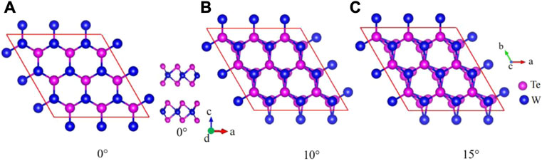
FIGURE 1. Top view of the twisted bilayer WTe2 crystal structure with twist angles of (A) 0°, (B) 10°, and (C) 15°. Side view of the twisted bilayer WTe2 corresponds to the twist angles of 0°. Blue and purple represent W and Te atoms, respectively.
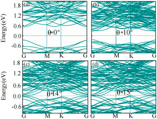
FIGURE 2. Band structures of bilayer WTe2 with twist angles (A) 0°, (B) 10°, (C) 14°, and (D) 15°. Specific torsional values are indicated accordingly in the plots. Light black dashed dots represent Fermi energy.
The valence-band maximum and conduction-band minimum for the systems of 0, 10, 14, and 15° are located at the G point. The bandgaps for non-twisted and twisted systems of 0, 10, 14 and 15° are different. The results show that the bandgap changes very significantly for larger twist angles from 0 to 15°. For example, for structures with a twist angle of 15°, the bandgap is zero. The change of the bandgap with the twist angle may be a common feature of the twisted structure WTe2, and significant changes in its luminescence properties are expected. Twists along the superposition direction change the interlayer distance and thus significantly alter the interlayer vdW interaction [22]. Previous studies have also found that twists can sensitively change the electronic properties of the edges of molybdenum disulfide [16–19, 22, 40].
From the aforementioned band structure diagram, we observe that the bandgap and ∆E vary with the twist angle. We present this regularity in the following, as shown in Figures 3A,B. The bandgap of WTe2 is very sensitive to the change of the twist angle. The bandgap changes accordingly as the twist angle changes continuously. The bandgap decreases trends from 0 to 15°. The bandgap determines the energy required for the valence-band electrons to leap to the conduction band. The larger the bandgap, the higher the leap energy, the less likely the electrons will be excited. Therefore, when the twist angle is from 0 to 15°, the bandgap shows an overall decrease tendency, which is favorable for the valence-band electrons to jump to the conduction band. When the twist angle is from 0 to 15°, the bandgap shows an overall decrease tendency, and the binding effect on the valence-band electrons is weaker, which is favorable for the valence-band electrons to get rid of the valence bonds and also favorable for conductivity. When the angle is turned to a particular angle, the appearance of the reduced bandgap may reduce the carrier, when the kinetic energy of the carrier is quenched, the enhanced electron–electron interaction may lead to the appearance of a strongly correlated phase [6, 41–44].
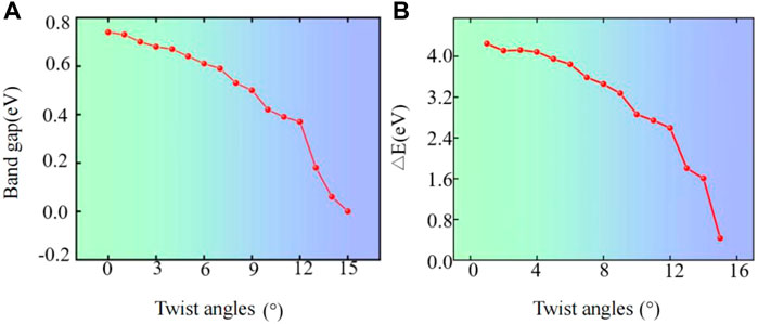
FIGURE 3. (A) Bandgap of bilayer WTe2 as a function of the twist angles. (B) ∆E (the total energy difference that is relative to the untwisted WTe2) as a function of the twist angles.
The ∆E varies with the twist angle trend of fluctuation and is very large. The ∆E of the twisted bilayer WTe2 is obtained by subtracting the energy without the twist angle from the energy after the twist angle. As the twist angle increases, the energy change of the twist angle also shows the result of certain changes. When the twist angle is from 0 to 15°, the energy tends to decrease overall. It can be seen from the relationship between ∆E and the twist angle as described before, as shown in Figure 3B. When the twist angle is 1°, the corresponding energy is the largest, which means that the system is the most unstable compared to twisted systems with other twisted angles. But when the twist angle is 15°, the corresponding energy is the smallest, which means that the system is the most stable compared to other twisted systems with other twisted angles.
We explain it in terms of the projected density of states (PDOS), as shown in Figures 4A,D. The PDOS of twisted bilayer WTe2 mainly has the d-orbitals of W and the p-orbitals of Te atoms as the contributions near the Fermi level. As the twist angle increases, the density of states moves toward the Fermi level and the bandgap of the system substantially decreases for 10, 14, and 15°. At 14°, the system shows an approximate zero bandgap state with a bandgap of only 0.07 eV, while at 15°, the bandgap of the system is completely closed and the system appears metallic.
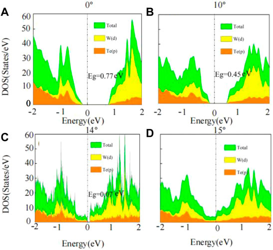
FIGURE 4. Projected density of states (PDOS) of WTe2 with and without twist angles. PDOS of twisted bilayer WTe2 with twist angles (A) 0°, (B) 10°, (C) 14°, and (D) 15°.
Interestingly, the PDOS are shown in Figures 4A,D. When the twist angle is turned from 0 to 15°, we derive that the PDOS is localized in peaks. This new localization significantly changes the transport properties [19–21, 45, 46]. Because of the localization of PDOS, there are sharp peaks at the Fermi level of the PDOS. The peaks of PDOS lead to a strong change in the density of states. As the twist angle increases, the sharp peaks move toward near the Fermi level, with the sharp peaks of 1.4 eV for a twist angle of 0°, 1.3 eV for a twist angle of 10°, 1.0 eV for a twist angle of 14°, and 0.9 eV for a twist angle of 15°. These peaks are due to the relatively localized electrons in the d-orbital of the W atom. We conjecture that the change of the bandgap is influenced by the changes of these peaks.
When the twist angle reaches 15°, the PDOS is localized compared to 0° twisted systems. When the twist angle reaches 15°, the appearance of sharp peaks near the Fermi level and the movement of electrons in the p-orbitals of the Te and d-orbitals of W atoms move toward near the Fermi level resulting in a bandgap of 0 eV. Therefore, the bandgap changes due to the electrons of the p-orbitals of Te and d-orbitals of W atoms move toward near the Fermi level, and there are sharp peaks near the Fermi level.
Next, we explain it in terms of the distance between Te and Te atoms, as shown in Figures 5A,B. As the twist angle increases, there is an overall tendency for the distance between Te and Te atoms to decrease when the twist angle is from 0 to 15°. The bandgap shows an overall decrease tendency when the twist angle is from 0 to 15°. Therefore, as the twist angle increases, the bandgap decreases as the distance between Te and Te atoms decreases when the twist angle is from 0 to 15°. The bandgap is affected as the overall distance between Te and Te atoms tends to decrease.
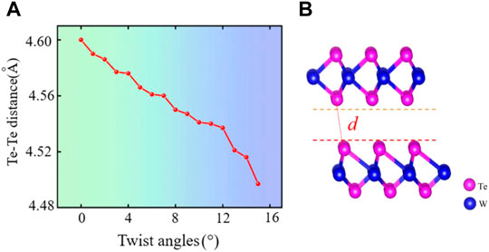
FIGURE 5. (A) Distance between Te and Te atoms as a function of twist angles. (B) Side view of WTe2, where d [d represents the Te–Te distance in Figure (B)] is the distance between Te and Te atoms.
Figure 6 depicts the charge density difference at the twisted bilayer WTe2 interlayer, which is defined by subtracting the charge density at the twist angle from the charge density without the twist angle. Finally, it is explained by the charge density difference, as shown in Figures 6A,B. With the increase of the twist angle, the electron gaining the ability of W atoms is enhanced, and the number of electrons gained is increased, which affects the change of bandgap due to the transfer of electrons. When the twist angle is 10°, the W atoms gain electrons. In the case of equal planes, it is advantageous for the W atoms, and the covalent bond is enhanced. When the twist angle is 15°, it is favorable for W atoms to gain electrons more easily.
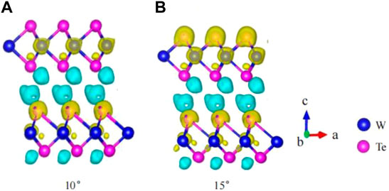
FIGURE 6. (A,B) Charge density difference with the charge density at 10° and 15° subtracting the charge density at 0°. The isosurface value is 7 × 10⁻² e per bohr3. The yellow isosurface indicates gained electrons, while the blue isosurface indicates lost electrons.
From Figure 6, we know that W atoms with 15° get more electrons than those of 10°. The charge density overlapping at a twist angle of 15° is more than that with the twist angle of 10°. So the bandgap of 15° is smaller than that of 10°. The bandgap at 10° is 0.45 eV, while the bandgap at 15° is zero. It means that the transfer of charge affects the bandgap.
In summary, we have performed first-principle calculations of the electronic structure of twisted bilayer WTe2. The bandgap is very sensitive to the variation of the twist angle. When the twist angle is 0°, the bandgap is the largest compared to other twisted systems, and the bandgap is a direct bandgap. However, when the twist angle is 15°, the bandgap is the smallest compared to other twisted systems, and the bandgap is a direct bandgap. Twist significantly changes the band structure resulting in bandgap engineering when the twisted bilayer WTe2 is turning to a specific angle. The calculations demonstrated that the twist significantly changes the band structure of the bandgap. A semiconductor-to-metal phase transition is found at 15°. The same VBM/CBM and the components of the orbitals near the Fermi level exhibit drastic change under twist. These significant changes near the Fermi level for a twisted system will result in a significant change in optical and electronic transport properties. Twisted layered materials have potential applications in future electronic devices. The realization of twisted layered materials provided a platform in the future to study strongly correlated superconducting behavior and the unconventional superconductivity of insulator states.
The original contributions presented in the study are included in the article/Supplementary Material, further inquiries can be directed to the corresponding authors.
KZ and J-MZ: conceived and supervised this work. Z-SC: performed the calculations. Z-SC and KZ: wrote the manuscript. LH, W-TG, and ZH: analyzed the data and provided valuable and constructive suggestions.
The authors declare that the research was conducted in the absence of any commercial or financial relationships that could be construed as a potential conflict of interest.
All claims expressed in this article are solely those of the authors and do not necessarily represent those of their affiliated organizations, or those of the publisher, the editors, and the reviewers. Any product that may be evaluated in this article, or claim that may be made by its manufacturer, is not guaranteed or endorsed by the publisher.
We acknowledge the financial support by the National Natural Science Foundation of China (Nos. 11874113 and 62174032), the Natural Science Foundation of Fujian Province of China (Nos. 2020J02018 and 2021J01189). The work was carried out at the National Supercomputer Center in Tianjin, and the calculations were performed on TianHe-1(A).
1. Wolf TMR, Lado JL, Blatter G, Zilberberg O. Electrically Tunable Flat Bands and Magnetism in Twisted Bilayer Graphene. Phys Rev Lett (2019) 123:096802. doi:10.1103/PhysRevLett.123.096802
2. Arora HS, Polski R, Zhang Y, Thomson A, Choi Y, Kim H, et al. Superconductivity in Metallic Twisted Bilayer Graphene Stabilized by WSe2. Nature (2020) 583:379–84. doi:10.1038/s41586-020-2473-8
3. Mao J, Milovanović SP, Anđelković M, Lai X, Cao Y, Watanabe K, et al. Evidence of Flat Bands and Correlated States in Buckled Graphene Superlattices. Nature (2020) 584:215–20. doi:10.1038/s41586-020-2567-3
4. Cao Y, Fatemi V, Fang S, Watanabe K, Taniguchi T, Kaxiras E, et al. Unconventional Superconductivity in Magic-Angle Graphene Superlattices. Nature (2018) 556:43–50. doi:10.1038/nature26160
5. Lu X, Stepanov P, Yang W, Xie M, Aamir MA, Das I, et al. Superconductors, Orbital Magnets and Correlated States in Magic-Angle Bilayer Graphene. Nature (2019) 574:653–7. doi:10.1038/s41586-019-1695-0
6. Cao Y, Fatemi V, Demir A, Fang S, Tomarken SL, Luo JY, et al. Correlated Insulator Behaviour at Half-Filling in Magic-Angle Graphene Superlattices. Nature (2018) 556:80–4. doi:10.1038/nature26154
7. Bistritzer R, MacDonald AH. Moiré Bands in Twisted Double-Layer Graphene. Proc Natl Acad Sci U.S.A (2011) 108:12233–7. doi:10.1073/pnas.1108174108
8. Goodwin ZAH, Corsetti F, Mostofi AA, Lischner J. Attractive Electron-Electron Interactions from Internal Screening in Magic Angle Twisted Bilayer Graphene. Phys Rev B (2019) 100:14. doi:10.1103/physrevb.102.081403
9. Zhang Y, Hou Z, Zhao YX, Guo ZH, Liu YW, Li SY. Correlation-induced valley Splitting and Orbital Magnetism in a Strain-Induced Zero-Energy Flat Band in Twisted Bilayer Graphene Near the Magic Angle. Phys Rev B (2020) 102:2469–9950. doi:10.1103/physrevb.102.081403
10. Kim K, Yankowitz M, Fallahazad B, Kang S, Movva HCP, Huang S, et al. van der Waals heterostructures with high accuracy rotational alignment. Nano Lett (2016) 16:1989–95. doi:10.1021/acs.nanolett.5b05263
11. Carr S, Massatt D, Fang S, Cazeaux P, Luskin M, Kaxiras E. Twistronics. Manipulating the Electronic Properties of Two-Dimensional Layered Structures through Their Twist Angle. Phys Rev B (2017) 95:6. doi:10.1103/physrevb.95.075420
12. Dos Santos JMBL, Peres NMR, Neto AHC. Graphene Bilayer with a Twist: Electronic Structure. Phys Rev Lett (2007) 99:256802. doi:10.1103/PhysRevLett.99.256802
13. Carr S, Fang S, Jarillo-Herrero P, Kaxiras E. Pressure Dependence of the Magic Twist Angle in Graphene Superlattices. Phys Rev B (2018) 98:5. doi:10.1103/PhysRevB.98.085144
14. Cao Y, Rodan-Legrain D, Rubies-Bigorda O, Park JM, Watanabe K, Taniguchi T, et al. Tunable Correlated States and Spin-Polarized Phases in Twisted Bilayer-Bilayer Graphene. Nature (2020) 583:215–20. doi:10.1038/s41586-020-2260-6
15. Cao Y, Luo JY, Fatemi V, Fang S, Sanchez-Yamagishi JD, Watanabe K, et al. Superlattice-induced Insulating States and valley-protected Orbits in Twisted Bilayer Graphene. Phys Rev Lett (2016) 117:116804. doi:10.1103/physrevlett.117.116804
16. Xie Y, Lian B, Jäck B, Liu X, Chiu C-L, Watanabe K, et al. Spectroscopic Signatures of many-body Correlations in Magic-Angle Twisted Bilayer Graphene. Nature (2019) 572:101–5. doi:10.1038/s41586-019-1422-x
17. Zondiner U, Rozen A, Rodan-Legrain D, Cao Y, Queiroz R, Taniguchi T, et al. Cascade of Phase Transitions and Dirac Revivals in Magic-Angle Graphene. Nature (2020) 582:203–8. doi:10.1038/s41586-020-2373-y
18. Venkateswarlu S, Honecker A, De Laissardière GT. Electronic Localization in Twisted Bilayer with Small Rotation Angle. Phys Rev B (2020) 102:12. doi:10.1103/physrevb.102.081103
19. N'Diaye AT, Bleikamp S, Feibelman PJ, Michely T. Two-dimensional Ir Cluster Lattice on a Graphene Moiré on Ir(111). Phys Rev Lett (2006) 97:215501. doi:10.1103/PhysRevLett.97.215501
20. Trambly de Laissardière G, Mayou D, Magaud L. Localization of Dirac Electrons in Rotated Graphene Bilayers. Nano Lett (2010) 10:804–8. doi:10.1021/nl902948m
21. Nayak PK, Horbatenko Y, Ahn S, Kim G, Lee J-U, Ma KY, et al. Probing Evolution of Twist-Angle-Dependent Interlayer Excitons in MoSe2/WSe2 van der Waals Heterostructures. ACS Nano (2017) 11:4041–50. doi:10.1021/acsnano.7b00640
22. Wu J, Meng L, Yu J, Li Y. A First‐Principles Study of Electronic Properties of Twisted MoTe 2. Phys Status Solidi B (2019) 257:1900412. doi:10.1002/pssb.201900412
23. Huang S, Ling X, Liang L, Kong J, Terrones H, Meunier V, et al. Probing the Interlayer Coupling of Twisted Bilayer MoS2 Using Photoluminescence Spectroscopy. Nano Lett (2014) 14:5500–8. doi:10.1021/nl5014597
24. Zhang Z, Wang Y, Watanabe K, Taniguchi T, Ueno K, Tutuc E, et al. Flat Bands in Twisted Bilayer Transition Metal Dichalcogenides. Nat Phys (2020) 16:1093–6. doi:10.1038/s41567-020-0958-x
25. Regan EC, Wang D, Jin C, Bakti Utama MI, Gao B, Wei X, et al. Mott and Generalized Wigner crystal States in WSe2/WS2 Moiré Superlattices. Nature (2020) 579:359–63. doi:10.1038/s41586-020-2092-4
26. Yuan L, Zheng B, Kunstmann J, Brumme T, Kuc AB, Ma C, et al. Twist-angle-dependent Interlayer Exciton Diffusion in WS2-WSe2 Heterobilayers. Nat Mater (2020) 19:617–23. doi:10.1038/s41563-020-0670-3
27. Liu Q, Li J-J, Wu D, Deng X-Q, Zhang Z-H, Fan Z-Q, et al. Gate-controlled Reversible Rectifying Behavior Investigated in a Two-Dimensional MoS2 Diode. Phys Rev B (2021) 104:045412. doi:10.1103/PhysRevB.104.045412
28. Fan Z-Q, Jiang X-W, Luo J-W, Jiao L-Y, Huang R, Li S-S, et al. In-plane Schottky-Barrier Field-Effect Transistors Based on 1 T/2 H Heterojunctions of Transition-Metal Dichalcogenides. Phys Rev B (2017) 96:165402. doi:10.1103/PhysRevB.96.165402
29. Tian W, Yu W, Liu X, Wang Y, Shi J. A Review of the Characteristics, Synthesis, and Thermodynamics of Type-II Weyl Semimetal WTe₂. Materials (Basel) (2018) 11:22. doi:10.3390/ma11071185
30. Bruno FY, Tamai A, Wu QS, Cucchi I, Barreteau C, de la Torre A, et al. Observation of Large Topologically Trivial Fermi Arcs in the Candidate Type-II Weyl semimetalWTe2. Phys Rev B (2016) 94:121112. doi:10.1103/physrevb.94.121112
31. Jiang Y, Lai X, Watanabe K, Taniguchi T, Haule K, Mao J, et al. Charge Order and Broken Rotational Symmetry in Magic-Angle Twisted Bilayer Graphene. Nature (2019) 573:91–5. doi:10.1038/s41586-019-1460-4
32. Kou L, Tang C, Zhang Y, Heine T, Chen C, Frauenheim T. Tuning Magnetism and Electronic Phase Transitions by Strain and Electric Field in Zigzag MoS2 Nanoribbons. J Phys Chem Lett (2012) 3:2934–41. doi:10.1038/s41586-019-1460-410.1021/jz301339e
33. Yun WS, Han SW, Hong SC, Kim IG, Lee JD. Thickness and Strain Effects on Electronic Structures of Transition Metal Dichalcogenides: 2H-MX2 Semiconductors (M = Mo, W; X = S, Se, Te). Phys Rev B (2012) 5:333051–5. doi:10.1103/PhysRevB.85.033305
34. Kresse G, Furthmüller J. Efficiency of Ab-Initio Total Energy Calculations for Metals and Semiconductors Using a Plane-Wave Basis Set. Comput Mater Sci (1996) 6:15–50. doi:10.1016/0927-0256(96)00008-0
35. BlÖchl PE. Projector Augmented-Wave Method. Phys Rev B (1994) 50:17953–79. doi:10.1103/PhysRevB.50.17953
36. Ernzerhof M, Burke K, Perdew JP. Long‐range Asymptotic Behavior of Ground‐state Wave Functions, One‐matrices, and Pair Densities. J Chem Phys (1996) 105:2798–803. doi:10.1063/1.472142
37. Perdew JP, Burke K, Wang Y. Generalized Gradient Approximation for the Exchange-Correlation Hole of a many-electron System. Phys Rev B (1996) 54:16533–9. doi:10.1063/1.47214210.1103/physrevb.54.16533
38. Dawson WG, Bullett DW. Electronic Structure and Crystallography of MoTe2and WTe2. J Phys C: Solid State Phys (1987) 20:6159–74. doi:10.1088/0022-3719/20/36/017
39. Cea T, Walet NR, Guinea F. Electronic Band Structure and Pinning of Fermi Energy to Van Hove Singularities in Twisted Bilayer Graphene: A Self-Consistent Approach. Phys Rev B (2019) 100:205113. doi:10.1103/physrevb.100.205113
40. Liang T, Phillpot SR, Sinnott SB. Erratum: Parametrization of a Reactive many-body Potential for Mo-S Systems. Phys Rev B (2009) 85:199903. doi:10.1103/PhysRevB.79.245110
41. Gonzalez-Arraga LA, Lado JL, Guinea F, San-Jose P. Electrically Controllable Magnetism in Twisted Bilayer Graphene. Phys Rev Lett (2017) 119:107201. doi:10.1103/physrevlett.119.107201
42. Lu N, Guo H, Zhuo Z, Wang L, Wu X, Zeng XC. Twisted MX2/MoS2heterobilayers: effect of van der Waals interaction on the electronic structure. Nanoscale (2017) 9:19131–8. doi:10.1039/c7nr07746g
43. Li F, Shi C, Wang D, Cui G, Zhang P, Lv L, et al. Improved Visible-Light Absorbance of Monolayer MoS2 on AlN Substrate and its Angle-dependent Electronic Structures. Phys Chem Chem Phys (2018) 20:29131–41. doi:10.1039/c8cp03908a
44. Wang Z, Chen Q, Wang J. Electronic Structure of Twisted Bilayers of Graphene/MoS2 and MoS2/MoS2. J Phys Chem C (2015) 119:4752–8. doi:10.1021/jp507751p
45. Roldán R, Silva-Guillén JA, López-Sancho MP, Guinea F, Cappelluti E, Ordejón P. Electronic Properties of Single-Layer and Multilayer Transition Metal Dichalcogenides MX2(M= Mo, W and X = S, Se). Ann Phys (2014) 526:347–57. doi:10.1002/andp.201400128
Keywords: twisted angle, WTe2, electronic structure, first-principle calculations, twisted bilayer
Citation: Chen Z-S, Huang L, Guo W-T, Zhong K, Zhang J-M and Huang Z (2022) Tunable Electronic Structure in Twisted Bilayer WTe2. Front. Phys. 10:879756. doi: 10.3389/fphy.2022.879756
Received: 20 February 2022; Accepted: 22 March 2022;
Published: 25 April 2022.
Edited by:
Gang Zhang, Institute of High Performance Computing, SingaporeReviewed by:
Mads Brandbyge, Technical University of Denmark, DenmarkCopyright © 2022 Chen, Huang, Guo, Zhong, Zhang and Huang. This is an open-access article distributed under the terms of the Creative Commons Attribution License (CC BY). The use, distribution or reproduction in other forums is permitted, provided the original author(s) and the copyright owner(s) are credited and that the original publication in this journal is cited, in accordance with accepted academic practice. No use, distribution or reproduction is permitted which does not comply with these terms.
*Correspondence: Kehua Zhong, a2h6aG9uZ0Bmam51LmVkdS5jbg==; Jian-Min Zhang, am16aGFuZ0Bmam51LmVkdS5jbg==
Disclaimer: All claims expressed in this article are solely those of the authors and do not necessarily represent those of their affiliated organizations, or those of the publisher, the editors and the reviewers. Any product that may be evaluated in this article or claim that may be made by its manufacturer is not guaranteed or endorsed by the publisher.
Research integrity at Frontiers
Learn more about the work of our research integrity team to safeguard the quality of each article we publish.