 Zhidong Wen1,2
 Haiyan Shi1Song Yue1Man Li1Zhe Zhang1,2Ran Wang1Qi Song3Ziye Xu3Zichen Zhang1*Yu Hou1*
- 1Microelectronics Instruments and Equipment R&D Center, Institute of Microelectronics, Chinese Academy of Sciences, Beijing, China
- 2School of Microelectronics, University of Chinese Academy of Sciences, Beijing, China
- 3International Research Centre for Nano Handling and Manufacturing of China, Changchun University of Science and Technology, Changchun, China
Black silicon is a promising and effective candidate in the field of photoelectric devices due to the high absorptance and broad-spectrum absorption property. The deposition around the processing area induced by the pressure of SF6, gravity, and the block of the processing chamber interferes the adjacent laser ablation and hampers uniform large-scale black silicon fabrication. To solve the problem, femtosecond laser- induced black silicon assisted with laser plasma shockwave cleaning is creatively proposed in our study. The results showed that higher, denser, and more uniform microstructures can be obtained than the conventional laser-induced method without laser cleaning. The average absorptance is 99.15% in the wavelength range of 0.3–2.5 µm, while it is more than 90% in the range of 2.5–20 µm. In addition, the scanning pitch dependence of surface morphology is discussed, and the better result is obtained in the range of 25–35 µm with 40-µm laser spot. Finally, a large-scale 50-mm × 50-mm black silicon with uniform microstructures was prepared by our method. It has been demonstrated that the deposition is effectively eliminated via our method, and the optical absorption is also enhanced significantly. It is of great significance for realizing large-scale preparation of photoelectric devices based on black silicon and lays the foundation for the development of laser-inducing equipment and industrial application.
Introduction
Light-trapping structures can improve the local resonance modes of light and the propagating light wavelength range in the material, which not only enhances absorption of light from near-ultraviolet to the near-infrared and improves photocurrent but also reduces materials used. Currently, various nanoscale light-capturing methods, including photonic crystals, plasmonic nanostructures, and nanoscale lines and gratings [1–3], have been investigated. Black silicon is fabricated with micro-, nano-, or micro–nano-scale structures [4, 5]. While the absorption of silicon is reduced abruptly due to the forbidden bandwidth when the light wavelength is more than 1,100 nm [6], a better optical absorption property is showed on the black silicon due to the multiple reflections between the microstructures and impurity doping, especially in the near-infrared band ranging from 1,100 nm to 2,500 nm [7, 8]. Since the first research about black silicon was reported from Harvard University in 1998 [9], extensive research has been conducted on this promising material. Consequently, black silicon is an effective and low-cost candidate compared with the other photoelectric materials.
Due to the high absorptance and broad-spectrum absorption property, black silicon is applied in many fields. About photocatalysis and photo-electrocatalysis [10, 11], B. Wang et al. [12] fabricated a plasmon-enhanced black silicon material to synthesize ammonia using photo-electrocatalysis in 2020. About photodetection [13, 14], Z. Qi et al. [15] fabricated a gold nanoparticle-modified silicon pyramid-shaped material that was able to enhance thermal electron NIR light detection in 2017. About solar cell [16–19], I. Putra et al. [20] made a B-Si solar cell by performing a silver-assisted chemical etching of the micro-pyramid on a silicon wafer to form a finer nanocolumn structure on the micro-pyramid in 2019. In short, black silicon has great potential in the field of optoelectronic devices.
Furthermore, how to fabricate the micro-nano structures to get a good optical property is a great challenge in the field of photoelectric devices. In the past several decades, there were many methods reported about the preparation of black silicon, including metal-assisted chemical etching (MACE) [21, 22], wet chemical etching [23], reactive ion etching (RIE) [24, 25], and laser processing [26–29]. The absorption result of samples treated with femtosecond laser in SF6 was superior to the results of samples using other methods [30]. Sulfur-hyperdoped silicon processed by ultrafast laser led to a wide continuous impurity band, which has a wide contribution of energy levels and gives rise to infrared absorptance. In addition, the laser technology was compatible with the CMOS processing and has the advantages of flexibility, simplicity, and precision. However, there was a problem in the processing industrially that a large amount of powder deposited on the processing area after the laser irradiation [31]. The particles splashed from the surface due to the laser energy deposit mostly on the sides of the processing row. It deteriorated microstructure morphology on the next row, leading to a worse optical property of the whole large-scale black silicon.
Currently, research related to black silicon mainly centers on a small point. It is attributed to the difficulty to realize large-scale uniformity of microstructures by femtosecond laser and the high cost of the laser-processing equipment. Laser cleaning is a novel surface cleaning technology, with the advantages [32] of environmental protection, non-contact, wide range of applications, high cleaning accuracy, etc. The laser cleaning technology is applied in many fields, including the removal of paint [33], rust, compounds [34], particles [35], and the protection of artifacts [36]. In our study, laser cleaning was used to remove the deposit and enhance the uniformity of large-scale black silicon.
In our study, to solve the problem of deposition and prepare large-scale black silicon, a method of laser induction assisted with laser plasma shockwave cleaning was investigated. Compared with the conventional process method, the addition of the laser cleaning technology was helpful to remove the deposition so that a better optical property of the microstructures was achieved. A series of experiment were conducted. Then the morphology and the absorption property were obtained. The results indicated that laser induction assisted with laser cleaning was an effective and low-cost method which could be applied to the preparation of large-scale black silicon industrially, especially for the application of solar energy sells and optoelectronic devices.
Materials and Methods
The N-type silicon wafers (111) with a thickness of 200 µm were used as samples in our experiments. The wafers were polished before laser processing. A 25-W, 515-nm femtosecond laser system with a duration of 400 fs and a repetition rate of 200 kHz was used to fabricate black silicon. In addition, the processing position of the samples was controlled precisely by an xyz motion platform and affiliated software.
Figure 1A shows the schematic diagram of the whole processing system used in our study. The laser beam was focused through the lens (with a focal length of 75 mm), and the laser spot with a diameter of 40 µm was irradiated on the silicon wafer. The sample was set in SF6 with a pressure of 67 kPa. The scanning speed was 20 mm/s, with a laser fluence of 7.96 J/cm2 during the inducing process, while it was 100 mm/s with a laser fluence of 3.98 J/cm2 in the laser cleaning process. In order to fabricate large-scale black silicon, several fixed spacing rows were designed via affiliated software first as shown in Figure 1A. The laser-inducing process and laser-cleaning process were conducted alternatively. The detailed process was as follows: 1) first, laser scans in a certain direction forming one laser-induced black silicon; 2) second, the adjacent scanning by laser cleaning with the same spacing row was conducted; 3) third, the laser- inducing process was repeated along the same path as the second step; and 4) finally, large-scale uniform black silicon was formed by repeating the aforementioned steps. Figures 1B,C show the difference between our method and the conventional laser induction method. In our experiments, different distances between the processing rows were tried to find better performances of the large-scale black silicon.
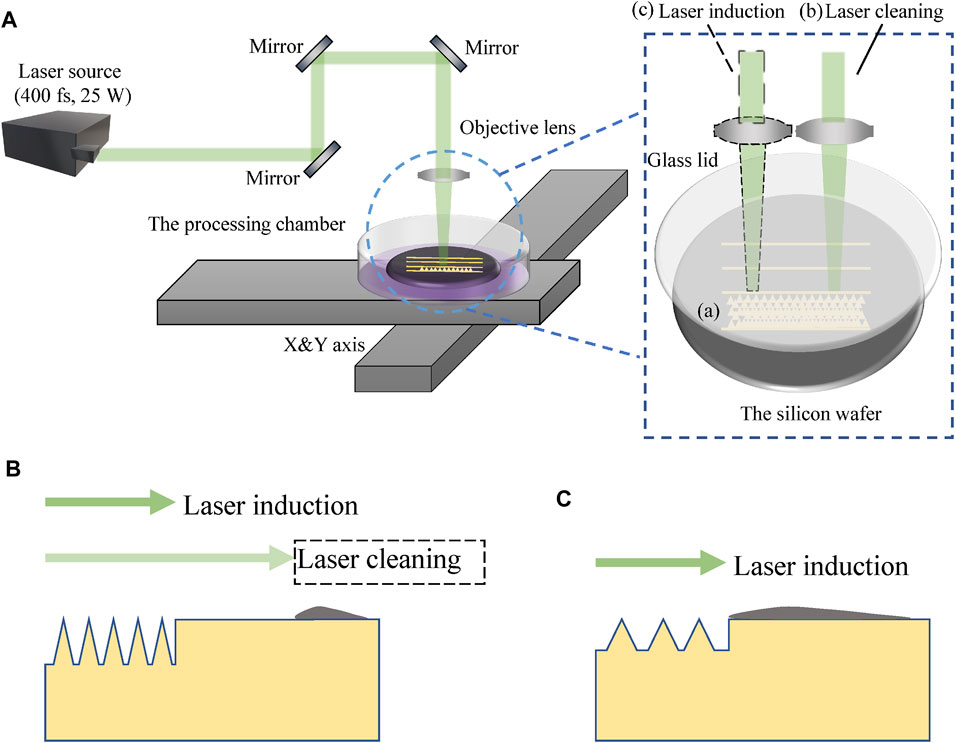
FIGURE 1. (A) Schematic diagram of the femtosecond laser processing system. (B) Laser induction assisted with laser cleaning and (C) conventional laser induction.
The morphology of the microstructures was characterized by the scanning electron microscope (SEM) and the laser-scanning confocal microscope. The 3D optical image was obtained from the laser-scanning confocal microscope to observe the whole morphology and calculate the RMS value. The color bar corresponded to the height of the model built in the 3D images. Furthermore, the absorptance of the treated samples in our study was analyzed using an ultraviolet spectrophotometer (for the wavelength range from 0.3 to 2.5 µm) and a Bruker Tensor–Fourier transform infrared (FTIR) spectrometer (for the wavelength range from 2.5 to 20 µm), both equipped with integrating spheres.
Results and Discussion
It was verified that the conical microstructures can be formed on the silicon material after pulsed laser processing in the gas of SF6. The powder splashed from the surface deposited on the sides of the processing line subsequently because of gravity, gas pressure, and the block of the glass cover. Figure 2 indicates the schematic diagram of the deposition laterally and the 3D image of a single row after the conventional laser-inducing process. The optical property and the microstructure of the fabricated black silicon were influenced. In order to remove the deposition, laser cleaning was conducted. The laser plasma shockwave cleaning has been an advanced and effective method to remove particles in recent years. Under the irradiation of the intense pulsed laser, the powder and the plasma plume were created [37]. The phenomena of gasification and ionization occurred in the plasma plume. Then, the plasma plume expanded rapidly with high temperature (>104 K) and high pressure (>1 GPa). Finally, the laser-heated plasma exploded and led to the formation of laser-supported detonation waves [38] to remove nanoparticles. The schematic diagram of the laser plasma shockwave cleaning is shown in Figure 3A. The detailed mechanism of laser cleaning is still a major research point. Figure 3B shows the result of Figure 2A processed after laser cleaning. The RMS value obtained from the laser scanning confocal microscope, which was the root mean square height for the evaluation area, was widely used to characterize the surface roughness. The RMS value for the non-cleaned region marked in red line in Figure 2A was 0.114 µm, while it was 0.054 µm for the cleaned area marked in Figure 3B. It is obvious that the deposition was eliminated effectively.
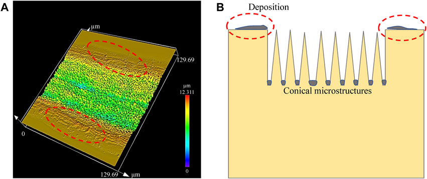
FIGURE 2. Deposition on the single row fabricated with laser inducing process. (A) 3D image of the processing row and (B) schematic of the deposition laterally.
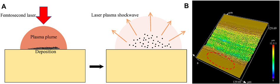
FIGURE 3. (A) Schematic diagram of the laser plasma shockwave cleaning and (B) result of Figure 2A processed with laser cleaning.
Figure 4 demonstrates the processed morphology prepared by laser-inducing process without laser cleaning and assisted with laser cleaning. The conical structures were formed in both processing methods. The microstructures in Figure 4B were denser and higher than the structures in Figure 4A. The RMS value for the area processed without laser cleaning was 1.71 µm, while it was 1.95 µm for the sample processed with laser cleaning. It is known that the better absorption property was attributed to the larger deep-to-width ratio and the multiple reflections between the conical structures [39]. The absorption curves of the processing area over the wavelength ranged from 300 nm to 20 µm and are illustrated in Figure 5. It is obvious that the absorptance of the samples prepared with laser cleaning was enhanced experimentally in the regions of ultraviolet, visible, near-infrared, and mid-infrared. In the wavelength range of 0.3–2.5 µm, the average absorption of the samples treated with laser cleaning was improved from 95.72 to 99.15%, while in the range of 2.5–20 μm, an average absorption of more than 90% was achieved in our experiments using the laser cleaning technology, which is the highest absorptance achieved on silicon by laser technology as far as we know.
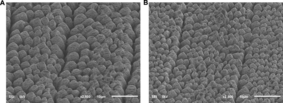
FIGURE 4. Surface morphology processed (A) without laser cleaning and (B) with laser cleaning.

FIGURE 5. Absorption curves of samples processed without laser cleaning and with laser cleaning.
In order to realize the industrial application of optoelectronic devices, it is necessary to improve the processing performance of large-scale black silicon prepared by the laser-inducing process assisted with laser cleaning. In our experiment, the different distances (5, 15, 25, 35, 45 µm) between adjacent rows were analyzed to improve the whole processing morphology. The 3D optical images of the samples are shown in Figure 6. The surfaces were ablated obviously, while the distance between rows was 5 µm or 15 µm because of the large overlapping laser energy, as shown in Figures 6A,B. Figure 6E shows that the energy deposited on the side of the rows was too little to induce the microstructures somewhere. As shown in Figures 6C,D, the 3D optical images show that the better microstructure morphology was obtained when the distance of rows was between 25 and 35 µm. The laser spot used in our study was 40 µm. In the fabrication of large-scale black silicon, different scanning pitches led to different overlapping rates of the laser spot and different energy irradiated on the silicon surface. An extremely small scanning pitch causes excessive laser energy on the irradiation area, while an extremely large pitch contributes too little energy to get the undesirable surface microstructure and worse optical properties. Therefore, an appropriate scanning pitch, which is related to the diameter of the laser spot and the laser fluence, should be selected in the laser processing of large-scale black silicon. Finally, the image of 50-mm × 50-mm black silicon prepared by femtosecond laser-inducing process assisted with laser cleaning is shown in Figure 6F. The scanning pitch between the adjacent rows was 25 µm. The processed area is shown in black completely due to its perfect light trapping.
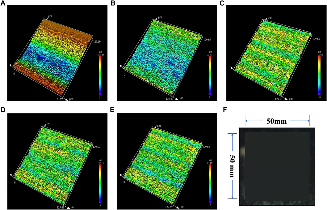
FIGURE 6. 3D images of samples with different pitches between rows, including (A) 5 μm, (B) 15 μm, (C) 25 μm, (D) 35 μm, and (E) 45 µm. (F) Image of 50-mm × 50-mm black silicon.
The method of the laser-inducing process assisted with laser plasma shockwave cleaning was certified previously to improve the optical property of large-scale black silicon. The laser cleaning technology was effective in removing the deposition beside the processing line and enhancing the density and uniformity of microstructures. In addition, the method assisted with laser cleaning was helpful in promoting the widespread application of photoelectric devices based on black silicon, especially in the field of mid-infrared. It also laid the foundation on the development and industrial application of laser-inducing equipment. However, the powder generated from the laser-cleaning and laser-inducing processes may redeposit on the previous processed area. The processing chamber prevents the powder from splashing out of the processing area. Further investigation is needed to reduce the influence of redeposition on the laser-induced surface and absorption property of black silicon.
Conclusion
In our study, the method of laser induction assisted with laser plasma shockwave cleaning in ambient SF6 to fabricate large-scale black silicon has been put forward. About this method, the femtosecond laser plasma shockwave cleaning technology was used to remove the deposition on the sides of processing rows before the next laser inducing.
In the laser-induced large-scale preparation of black silicon industrially, the particles deposit around the processing area induced by the gas pressure, gravity, and the block of the processing chamber. A set of experiments has been carried out to confirm the effectiveness of our method. In our experiments, the analysis of the SEM images and the 3D optical images indicated that the microstructures prepared by our method were denser and more uniform than the traditional laser-inducing process. The RMS value of the microstructures with this method was approximately 0.2 µm higher than the result without laser cleaning. Furthermore, great enhancement of the absorptance over a broad range was achieved significantly. In the wavelength range of 0.3–2.5 µm, the average absorption was 99.15%, and in the range of 2.5–20 μm, an absorptance of more than 90% has been realized experimentally. The absorptance is the highest compared with the results reported in other research as far as we know. Different scanning distances including 5, 15, 25, 35, and 45 µm with a 40-µm laser spot were conducted to get better microstructures. The best morphology was obtained with the processing pitches of 25 and 35 µm. Excessive overlapping laser energy led to the ablation of the surface of silicon, while too little overlapping laser energy induced to an undesirable morphology between the adjacent rows. Moreover, high-performance black silicon with a size of 50 mm × 50 mm was fabricated in our experiments.
The laser-inducing process assisted with laser plasma shockwave cleaning provides an effective and low-cost solution to eliminate the deposition in laser-induced large-scale black silicon. It is helpful to the development of optoelectronic devices, especially in the field of photocatalysis and photo-electrocatalysis, near-infrared and visible light photodetection, solar cell, sensing, antibacterial materials, and so on. Also, the method promotes the development and widespread application of femtosecond laser equipment.
Data Availability Statement
The original contributions presented in the study are included in the article/Supplementary Material, further inquiries can be directed to the corresponding authors.
Author Contributions
ZW, YH, and ZZ proposed the idea. ZW, YH, and ZZ performed the experiments. ZW, HS, ML, RW, QS, and ZX investigated the research progress. ZW, HS, SY, and YH wrote the original manuscript. YH, ZZ, ML, RW, and SY supervised the project.
Funding
This research was supported by the Beijing Municipal Science and Technology Commission (no. Z211100004821002).
Conflict of Interest
The authors declare that the research was conducted in the absence of any commercial or financial relationships that could be construed as a potential conflict of interest.
Publisher’s Note
All claims expressed in this article are solely those of the authors and do not necessarily represent those of their affiliated organizations, or those of the publisher, the editors, and the reviewers. Any product that may be evaluated in this article, or claim that may be made by its manufacturer, is not guaranteed or endorsed by the publisher.
References
1. Ferry VE, Polman A, Atwater HA. Modeling Light Trapping in Nanostructured Solar Cells. Acs Nano (2011) 5(12):10055–64. doi:10.1021/nn203906t
2. Hsu C-M, Battaglia C, Pahud C, Ruan Z, Haug F-J, Fan S, et al. High-Efficiency Amorphous Silicon Solar Cell on a Periodic Nanocone Back Reflector. Adv Energ Mater. (2012) 2(6):628–33. doi:10.1002/aenm.201100514
3. Kim Y, Bicanic K, Tan H, Ouellette O, Sutherland BR, García de Arquer FP, et al. Nanoimprint-Transfer-Patterned Solids Enhance Light Absorption in Colloidal Quantum Dot Solar Cells. Nano Lett (2017) 17(4):2349–53. doi:10.1021/acs.nanolett.6b05241
4. Lv J, Zhang T, Zhang P, Zhao Y, Li S. Review Application of Nanostructured Black Silicon. Nanoscale Res Lett (2018) 13:13. doi:10.1186/s11671-018-2523-4
5. Juzeliu̅nas E, Fray DJ. Silicon Electrochemistry in Molten Salts. Chem Rev (2020) 120(3):1690–709. doi:10.1021/acs.chemrev.9b00428
6. Casalino M, Coppola G, Iodice M, Rendina I, Sirleto L. Near-Infrared Sub-bandgap All-Silicon Photodetectors: State of the Art and Perspectives. Sensors (2010) 10(12):10571–600. doi:10.3390/s101210571
7. Loudon AY, Hiskett PA, Buller GS, Carline RT, Herbert DC, Leong WY, et al. Enhancement of the Infrared Detection Efficiency of Silicon Photon-Counting Avalanche Photodiodes by Use of Silicon Germanium Absorbing Layers. Opt Lett (2002) 27(4):219–21. doi:10.1364/ol.27.000219
8. Younkin R, Carey JE, Mazur E, Levinson JA, Friend CM. Infrared Absorption by Conical Silicon Microstructures Made in a Variety of Background Gases Using Femtosecond-Laser Pulses. J Appl Phys (2003) 93(5):2626–9. doi:10.1063/1.1545159
9. Her T-H, Finlay RJ, Wu C, Deliwala S, Mazur E. Microstructuring of Silicon with Femtosecond Laser Pulses. Appl Phys Lett (1998) 73(12):1673–5. doi:10.1063/1.122241
10. Alexander F, AlMheiri M, Dahal P, Abed J, Rajput NS, Aubry C, et al. Water Splitting TiO2 Composite Material Based on Black Silicon as an Efficient Photocatalyst. Solar Energ Mater Solar Cell (2018) 180:236–42. doi:10.1016/j.solmat.2017.05.024
11. Zhao S, Yuan G, Wang Q, Liu W, Wang R, Yang S. Quasi-hydrophilic Black Silicon Photocathodes with Inverted Pyramid Arrays for Enhanced Hydrogen Generation. Nanoscale (2020) 12(1):316–25. doi:10.1039/c9nr06635g
12. Wang B, Yao L, Xu G, Zhang X, Wang D, Shu X, et al. Highly Efficient Photoelectrochemical Synthesis of Ammonia Using Plasmon-Enhanced Black Silicon under Ambient Conditions. ACS Appl Mater Inter (2020) 12(18):20376–82. doi:10.1021/acsami.0c00881
13. Juntunen MA, Heinonen J, Laine HS, Vahanissi V, Repo P, Vaskuri A, et al. N-type Induced junction Black Silicon Photodiode for UV Detection. In: Conference on Integrated Photonics - Materials, Devices, and Applications IV; 2017 May 09-10; Barcelona, SPAIN (2017).
14. Meng Y, An L, Han X, Li Y, Hou C, Zhang Q, et al. Controllable (Ga1−xZnx)(N1−xOx) Nanorods Grown on Black Silicon as Anodes for Water Splitting. Appl Surf Sci (2020) 502:144174. doi:10.1016/j.apsusc.2019.144174
15. Zhou Z-Q, Wang L-X, Shi W, Sun S-L, Lu M. A Synergetic Application of Surface Plasmon and Field Effect to Improve Si Solar Cell Performance. Nanotechnology (2016) 27(14):145203. doi:10.1088/0957-4484/27/14/145203
16. Guenther KM, Baumann AL, Gimpel T, Kontermann S, Schade W. Yyyy Tandem Solar Cell Concept Using Black Silicon for Enhanced Infrared Absorption. In: 2nd International Conference on Crystalline Silicon Photovoltaics (SiliconPV); 2012 Apr 03-05; Leuven, BELGIUM. IMEC (2012).
17. Zhong S, Liu B, Xia Y, Liu J, Liu J, Shen Z, et al. Influence of the Texturing Structure on the Properties of Black Silicon Solar Cell. Solar Energ Mater Solar Cell (2013) 108:200–4. doi:10.1016/j.solmat.2012.10.001
18. Li P, Wei Y, Zhao Z, Tan X, Bian J, Wang Y, et al. Highly Efficient Industrial Large-Area Black Silicon Solar Cells Achieved by Surface Nanostructured Modification. Appl Surf Sci (2015) 357:1830–5. doi:10.1016/j.apsusc.2015.10.035
19. Abdullah MF, Alghoul MA, Naser H, Asim N, Ahmadi S, Yatim B, et al. Research and Development Efforts on Texturization to Reduce the Optical Losses at Front Surface of Silicon Solar Cell. Renew Sustain Energ Rev (2016) 66:380–98. doi:10.1016/j.rser.2016.07.065
20. Putra IR, Li J-Y, Chen C-Y. 18.78% Hierarchical Black Silicon Solar Cells Achieved with the Balance of Light-Trapping and Interfacial Contact. Appl Surf Sci (2019) 478:725–32. doi:10.1016/j.apsusc.2019.02.001
21. Cheng S-Q, Cai B, Zhu Y-M. Black Silicon as Absorber for Near-Infrared Photo-Thermal Conversion. In: Opto Electronics Communications Conference (OECC); 2015 Jun 28-Jul 02; Shanghai, PEOPLES R CHINA. IEEE (2015).
22. Phan TL, Yu WJ. CVD-grown Carbon Nanotube Branches on Black Silicon Stems for Ultrahigh Absorbance in Wide Wavelength Range. Sci Rep (2020) 10(1):10. doi:10.1038/s41598-020-60580-8
23. Tan Q, Tang L, Mao H, Chen Y, Ren Y, Lei C, et al. Nanoforest of Black Silicon Fabricated by AIC and RIE Method. Mater Lett (2016) 164:613–7. doi:10.1016/j.matlet.2015.11.062
24. Hildebrandt M, Hildebrandt M, Lu M. Self-organized Antireflecting Nano-Cone Arrays on Si (100) Induced by Ion Bombardment. J Appl Phys (2011) 109(5):053513. PubMed PMID: WOS:000288387900036. doi:10.1063/1.3560539
25. Qiu Y, Hao H-C, Zhou J, Lu M. A Close to unity and All-Solar-Spectrum Absorption by Ion-Sputtering Induced Si Nanocone Arrays. Opt Express (2012) 20(20):22087–94. doi:10.1364/oe.20.022087
26. Vorobyev AY, Guo C. Direct Creation of Black Silicon Using Femtosecond Laser Pulses. Appl Surf Sci (2011) 257(16):7291–4. doi:10.1016/j.apsusc.2011.03.106
27. Huang Z-M, Huang W-Q, Jiang Z-M, Liu S-R, Wu X-K, Qin C-J. Electronic States of Defect with Impurity and Infrared Emission on Black Silicon Prepared by an Ns-Laser. Opt Lett (2017) 42(2):358–61. doi:10.1364/ol.42.000358
28. Zhao J-H, Lv Z-H, Li C-H, Yu X-Y, Li X-B. The Infrared Photodiode of Textured Silicon Irradiated under Mixed Gas by Femtosecond Laser. IEEE Sensors J (2016) 17(4):1. doi:10.1109/jsen.2016.2638434
29. Su Y, Zhan X, Zang H, Fu Y, Li A, Xu H, et al. Direct and Stand-Off Fabrication of Black Silicon with Enhanced Absorbance in the Short-Wavelength Infrared Region Using Femtosecond Laser Filament. Appl Phys B (2018) 124(11). doi:10.1007/s00340-018-7092-9
30. Fan Z, Cui D, Zhang Z, Zhao Z, Chen H, Fan Y, et al. Recent Progress of Black Silicon: From Fabrications to Applications. Nanomaterials (2021) 11(1):41. doi:10.3390/nano11010041
31. Chen T, Wang W, Tao T, Mei X, Pan A. Deposition and Melting Behaviors for Formation of Micro/nano Structures from Nanostructures with Femtosecond Pulses. Opt Mater (2018) 78:380–7. doi:10.1016/j.optmat.2018.02.051
32. Gradini R, Chen F, Tan R, Newlin L. A Summary on Cutting Edge Advancements in Sterilization and Cleaning Technologies in Medical, Food, and Drug Industries, and its Applicability to Spacecraft Hardware. Life Sci Space Res (2019) 23:31–49. doi:10.1016/j.lssr.2019.05.002
33. Madhukar YK, Mullick S, Nath AK. Development of a Water-Jet Assisted Laser Paint Removal Process. Appl Surf Sci (2013) 286:192–205. doi:10.1016/j.apsusc.2013.09.046
34. Xie X, Huang Q, Long J, Ren Q, Hu W, Liu S. A New Monitoring Method for Metal Rust Removal States in Pulsed Laser Derusting via Acoustic Emission Techniques. J Mater Process Tech (2020) 275:116321. doi:10.1016/j.jmatprotec.2019.116321
35. Jia B, Miao X, Jiang Y, Tang H, Yao C. Cleaning of Graphite Particles Embedded in the Surface of Ductile Iron by Using a Novel Method. Math Probl Eng (2021) 2021:1–9. doi:10.1155/2021/6664916
36. Rivas T, Pozo-Antonio JS, López de Silanes ME, Ramil A, López AJ. Laser versus Scalpel Cleaning of Crustose Lichens on Granite. Appl Surf Sci (2018) 440:467–76. doi:10.1016/j.apsusc.2018.01.167
37. Wu J, Zhao J, Qiao H, Hu X, Yang Y. The New Technologies Developed from Laser Shock Processing. Materials (2020) 13(6):1453. doi:10.3390/ma13061453
38. Harilal SS, Miloshevsky GV, Diwakar PK, LaHaye NL, Hassanein A. Experimental and Computational Study of Complex Shockwave Dynamics in Laser Ablation Plumes in Argon Atmosphere. Phys Plasmas (2012) 19(8):083504. doi:10.1063/1.4745867
Keywords: large scale, laser cleaning, deposition, black silicon, laser inducing
Citation: Wen Z, Shi H, Yue S, Li M, Zhang Z, Wang R, Song Q, Xu Z, Zhang Z and Hou Y (2022) Large-Scale Black Silicon Induced by Femtosecond Laser Assisted With Laser Cleaning. Front. Phys. 10:862605. doi: 10.3389/fphy.2022.862605
Received: 26 January 2022; Accepted: 04 March 2022;
Published: 25 March 2022.
Edited by:
Shangran Xie, Beijing Institute of Technology, ChinaReviewed by:
Pan Wang, Nankai University, ChinaAlpan Bek, Middle East Technical University, Turkey
Qing Wang, Beijing Institute of Technology, China
Copyright © 2022 Wen, Shi, Yue, Li, Zhang, Wang, Song, Xu, Zhang and Hou. This is an open-access article distributed under the terms of the Creative Commons Attribution License (CC BY). The use, distribution or reproduction in other forums is permitted, provided the original author(s) and the copyright owner(s) are credited and that the original publication in this journal is cited, in accordance with accepted academic practice. No use, distribution or reproduction is permitted which does not comply with these terms.
*Correspondence: Zichen Zhang, enoyNDFAaW1lLmFjLmNu; Yu Hou, aG91eXVAaW1lLmFjLmNu