 R. Brunetti
 C. Jacoboni1
 E. Piccinini
95% of researchers rate our articles as excellent or good
Learn more about the work of our research integrity team to safeguard the quality of each article we publish.
Find out more
ORIGINAL RESEARCH article
Front. Phys. , 06 April 2022
Sec. Interdisciplinary Physics
Volume 10 - 2022 | https://doi.org/10.3389/fphy.2022.854393
This article is part of the Research Topic Emerging Non-Volatile Memories and Beyond: From Fundamental Physics to Applications View all 5 articles
A space- and time-dependent theoretical model based on a trap-assisted, charge-transport framework for the amorphous phase of a chalcogenide material is used here to interpret available experimental results for the electric current of nanoscale devices in the ns–ps time domain. A numerical solution of the constitutive equations of the model for a time-dependent bias has been carried out for GST-225 devices. The “intrinsic” rise time of the device current after the application of a suitable external bias is controlled by the microscopic relaxation of the mobile-carrier population to the steady-state value. Furthermore, the analysis is extended to include the effect of the external circuit on the electrical switching. A quantitative estimate of the current delay time due to unavoidable parasitic effects is made for the optimised electrical set up configurations recently used by experimental groups.
Chalcogenide-based Phase Change Memories (PCM) have been studied for many years as a possible replacement for Flash memories, and in the late 2000s eventually hit the market as storage elements for cell phones [1]. Furthermore, being two-terminal devices incorporating selectors made of materials belonging to the chalcogenide class [2], they were easily integrated in 3D cross-point memory arrays [3–5], paving the way for storage-class memories thanks to their fast access time and moderate cost per bit.
After a suitable tailoring of the chalcogenide-alloy composition, to match the specs dictated by a specific use, embedded PCM have the potential to become key enablers of technological breakthroughs in a number of industrial applications; among these, automotive applications [6]. In recent years, PCM devices were also profitably employed in “non von Neumann” neuromorphic computing architectures, exhibiting a better performing collocation of memory and processing [7–10].
Whatever application for PCM devices is envisaged, their working principle relies on the fast and reversible structural change of a chalcogenide alloy that switches between the amorphous (reset) and crystalline (set) states, upon the application of an electric pulse [11–14]. In many cases, a voltage pulse of suitable intensity, and width of a few ns is required to surpass, first, an Ovonic Threshold Switching (OTS) event, namely an off-to-on threshold switching in the amorphous state, precursor of the amorphous-to-crystalline phase change. As pointed out by many scientists [15–17], the lower limits of a fast electrical switching for both selectors and memory elements based on chalcogenides are related to the above-described transition from low-to high-conductivity states of the amorphous phase, and to the crystallization kinetics starting from the amorphous phase [16].
On the theoretical side, even though the first speculations date back to the 1970s [18], the scientific debate is still alive even 40 years later [12]; accurate and handy ab-initio molecular-dynamics simulations and/or density-functional calculations for a number of chalcogenide alloys have been published only recently. They allow one to speculate about the connection between the change of conductivity observed when OTS (and, subsequently, phase change) sets in, and the structural changes of the materials at the atomic level induced by the application of an external bias. Even though the quantitative results depend on the types of atoms forming the particular alloy and on the alloy stoichiometry, some interesting general concepts have been evidenced. A large conduction-band tail of localized states is detected in Ge-rich GexSe1−x and in similar systems [19,20]; this is correlated to the nonlinear conduction features of OTS, whereas in Se-rich Ge30Se70 the Ge valence-alternating pairs and Se lone pairs dominate [20]. A different interpretation has been proposed based on the so-called metavalent bond; specifically, the extent of localization of electronic states is found to depend on the applied electric field: localized states of the amorphous chalcogenide transform into extended states [21,22], this eventually reducing the amount of charge traps and increasing the electric conductivity. However, the direct in situ observation of the above-mentioned structural features of the OTS switching still remains a challenge due to technological limitations.
A useful parameter that has been introduced by experimentalists to quantify the transition speed is the so-called delay time td, defined as the time interval between the instant at which the applied voltage exceeds the threshold value and the instant at which a steep rise in the device current begins [23,24]. Despite efforts to decrease td with different strategies, so far it has been difficult to obtain values below 1 ns [23]. Thus, achieving sub ns threshold-switching times for nanoscale devices is a goal of both scientific and technological relevance [23,25].
The exploitation of the electrical threshold switching property of many chalcogenide-based devices, for designing phase-change memory devices with access speed comparable to the SRAM, pushed experimentalists to design accurate measuring setups [26]. The latter must be able to respond to very fast external electric pulses, in order to precisely record the onset of the threshold switching and the change of the current value from the low value of the amorphous off state to the high value of the amorphous on state. A major attempt to provide new experimental insights into the threshold-switching mechanism by means of a precise knowledge of the exact shape of the voltage applied to the chalcogenide cell has been carried out by Salinga and coworkers [23]. According to the Authors, in the reported experiments on GST-225 devices, due to the careful impedance matching of the contact board the applied voltage pulses reach the memory cell without any significant distortion. Measurements were performed where the applied voltage signal, aimed at producing the threshold voltage, ramps up linearly from zero to a maximum value; the leading edge of the voltage ranges from few ns to 104 ns. The value at which threshold switching appears depends upon the steepness of the ramp; in particular, short rise times of the latter lead to high switching voltages, whereas the application of slow ramps produces a decrease in the switching voltage. Thus, the pulse shape strongly influences the switching voltage, so that the concept of a unique voltage at which the resistance of the cell falls becomes questionable [23,24].
This concept is pushed even further in a recent paper by Saxena and coworkers [25], where it is shown that delay times in the ps scale can be obtained in GST-225 cells by means of an appropriate design of both the experimental apparatus and the external voltage applied to the cell. In particular, the Authors measured delay times shorter than 50 ps for a voltage equal to twice the threshold voltage measured in static conditions for the same material, proving that PCM memory devices can reach SRAM-like speeds. Besides the technological implications of the above-mentioned performances, experimental measurements of Ovonic threshold switching in the time domain provide new interpretation challenges to test the existing theories about the switching mechanism; such theories have been formulated mainly by Academia over the last 5 decades in parallel with the technological developments. While, in the low-resistance state, the standard description of conduction in semiconductors applies, the electric properties of the high-resistance state are explained as a hot-carrier effect [27–30], or a combination of electro-thermal effects [31,32]. Experiments where the parasitic effects have been reduced as much as possible confirm the relevance of hot-carrier phenomena on OTS, even though the high thermal efficiency and the fast thermal dynamics in nanoscale devices suggest that the heat flow dynamics can indeed play a role [32].
As for the OTS effect in the amorphous phase, structural analyses and Molecular-Dynamics simulations of amorphous chalcogenides confirm the existence of a number of trap states located around mid gap, that play a fundamental role on the onset of the electrical switch [13,14]. At low fields (below threshold) the majority of carriers are trapped and the conduction is very low; when the field is strong enough to heat the carriers, the population of the high-energy, high-mobility states is enhanced. This, in turn, increases the energy gain of the trapped carriers at the expense of the field, further enriching the population of the trap states close to the conduction-band edge (and, possibly, also band states [30]): in this way a positive feedback is established which, eventually, makes the current to increase by several orders of magnitude.
In this paper we apply a space- and time-dependent theoretical model based on a trap-assisted charge transport in the amorphous phase of a chalcogenide material [33,34], to interpret the available experimental results in the ns–ps time domain for the electric current of nanoscale devices, based on the GST-225 chalcogenide, in a variety of bias conditions. A numerical solution of the constitutive equations of the model for a time-dependent bias makes it possible to test to what extent the threshold voltage depends upon the microscopic characteristic times that regulate the field-to-carrier energy transfer; this transfer is in fact responsible for the carrier heating which, in turn, produces the threshold switching. Furthermore, the analysis is extended to include the effect of the external circuit on the electrical switching, with reference to the optimised electrical set up configurations recently used by experimental groups [25].
Section 2 summarizes the main features of the theoretical approach; the set of equations which constitute the model for the OTS device, and the numerical algorithm implemented for solving them, are described in Sections 2.1–2.3, while Section 2.4 illustrates how we modeled the OTS device coupling with an external circuit that represents the measuring equipment. Dynamic and static models for the OTS device have been tested in view of their possible implementation into a device simulation framework. Section 3 contains our results and their critical analysis: first, parasitic effects are neglected; the ideal cases of a voltage step (Section 3.1) and of voltage trapezoidal profiles, similar to those reported in [25], are considered with the purpose of evaluating the delay time of the OTS device (Section 3.2); then, the more realistic condition of a voltage trapezoidal profile applied to a device in presence of parasitic effects is studied (Section 3.3). Finally, Section 4 summarises the main achievements of the analysis, and provides some comments about possible developments of the present approach.
The analysis aims at interpreting the experimental current-voltage curves obtained by applying time-dependent voltages with a time scale ranging from the nanoseconds to the picoseconds. Based on a thorough study of the Ovonic threshold switching by the Authors of the present paper and others [27,33,34], the theoretical approach assumes that, when the chalcogenide material is in the amorphous phase, carrier heating due to energy transfer from the external field dominates over thermal effects in determining the OTS. Accordingly, the heat equation for the lattice is not included in the model.
The experimental evidence is for a unipolar conduction in GST-225 ([14], Ch. 2). This suggests that carrier excitation from trap to band states prevails over carrier transfer from the valence to the conduction band via trap states in the energy gap [18]. The present model equally applies to electrons or holes; for the sake of simplicity we developed and discussed the model only for the case of electrons. Carriers can occupy two trap levels with energy values ET = 0 and EB = Δ, with density of states gT and gB, respectively. Carriers in level ET are trapped, i.e., have zero mobility and, therefore, do not contribute to the current; carriers in level EB mimic conduction electrons, even though they have a unique well-defined energy, and contribute to the current with a constant mobility μ. The use of a single energy level for the mobile states is in fact a simplification of the model; however, a sensible description of the physics is anyway achieved [33]. The introduction of a dispersion relation of the mobile states improves the quantitative description of the electric switching at and above threshold, without altering the key features of the present implementation [30].
The device dynamics is assumed to be one-dimensional: the cross section of the sample is supposed large enough to neglect the effects of the lateral boundaries. Thus, the physical quantities of interest along the device are functions only of the longitudinal coordinate x and of time t; they are the electric field F, the total concentration of carriers n, the concentration of mobile carriers nB, the concentration of carriers in the trap states nT, and the particle current density j. The above quantities are not all independent from each other; in fact,
where DB is the diffusion coefficient of the mobile electrons, assumed here to be given by the equilibrium Einstein relation DB = μ k T0/q, with q the carrier charge, T0 the room temperature, and k the Boltzmann constant. At equilibrium, the device is assumed to be spatially uniform, with an electron density n0 neutralized by an equal density of opposite fixed charges. Furthermore, assuming Maxwellian distributions, the densities of carriers in the traps and in the mobile states are given by
The normalization constant C0 is obtained from the total electron density n0, leading to:
In presence of an electric field F (x, t), electrons gain energy; furthermore, the excitation energy to reach the upper level is reduced by the field according to the Poole model [35], to become
with γ a suitable constant1. Out of equilibrium we assume that an electron temperature Te (x, t) is defined, such that the electron populations, in analogy with Eq. 3, read
It is worth noting that a variation of the electric field F (x, t) is instantaneously accompanied by a variation of the activation energy Δ′, while the carriers require some time to adjust their occupations to the new situation. Thus, the above quantities
The model is based on a set of four differential equations, each encoding a basic physical principle.
i. Particle continuity: only charges in the mobile states can move, so that the rate of change of electron density at a given position x reads:
ii. Local particle redistribution: as indicated in Eq. 6, particles that cross the device at the position x come from mobile states. The rate of change of the concentration nB accounts for redistribution between trap and mobile states, and reads
where τn is the mobile-carrier relaxation time, taken as a model parameter, and
iii. Energy continuity: the energy density ϵt at (x, t) is given by nB Δ since ET = 0. Its variation accounts for the power density pumped by the field, the space variation of the energy flux j Δ, and the energy relaxed to the phonon bath which, in this case, is described by a temperature-relaxation time τT [29]:
On the other hand, differentiating the total energy ϵt (x, t) = nB Δ, and using Eq. 7, yields
Combining this result with Eq. 8 and using Eq. 6 provides
This equation indicates that the power provided by the field is partially dissipated to the phonon bath, and partially devoted to distribute the electrons between trapped and mobile states. This equation allows for the evaluation of the electron temperature in terms of the other unknowns. However, Te appears also in
iv. Poisson equation: the local carrier density n (x, t) is related to the local field F (x, t) by the Poisson equation:
where ɛ is the material’s absolute permittivity.
It is worth observing that in steady state the second term at the right hand side of Eq. 9 vanishes due to Eq. 7; it follows that τn has no influence on the steady-state behavior of the OTS device (more comments on this are made in Section 3.1).
The four Eqs. 6, 7, 9, 10 govern the process we are interested in, and are solved, e.g., for the unknowns n, F, nB, and Te. All other variables of interest can be calculated from the set above. A number of conditions are imposed on the unknowns:
a) The electron temperature at the injecting contact is equal to the equilibrium temperature at all times:
b) At the source boundary of the device, the contact injects the electrons which are necessary to maintain local electric neutrality at all times:
which implies:
(the second of the above derives from Eq. 10). Finally
c) an integral condition on the field is imposed by the voltage VP(t) across the device:
where L is the device length.
The model illustrated above is of the hydrodynamic type, namely, it assumes that neither the lattice temperature nor the relaxation time τT vary within the operating time scale of the device. This is justified by the fact that the effects of lattice heating can be neglected below threshold and do not alter the intrisic time scale of the device above threshold [33].
The non-linear system of equations outlined in Sections 2.1, 2.2 is solved by iterations, starting from the equilibrium condition n (x, 0) = n0, F (x, 0) = 0,
1. The update n (x, t + δt) is derived from Eq. 6.
2. Equations 5 and 7 provide the update nB (x, t + δt).
3. The update F (x, t + δt) is obtained from Eq. 10 apart from the constant F (0, t), which is found by imposing condition Eq. 13. The latter, in turn, is to be considered as prescribed if the device is in a standalone situation, that is, connected to a voltage generator; if, instead, the device is connected to an external circuit, VP must be derived from the solution of the device-circuit system.
4. The update Te (x, t + δt) is obtained from Eq. 9. Due to the strong non-linearity of this equation and the strict requirement of a positive solution, the combined bracketing and bisection techniques ([36], Section 9.1) proved to be more efficient and stable than other iterative methods like, e.g., the Newton-Raphson method.
In realistic conditions, the device under investigation is coupled with an external circuit that represents the measuring equipment. Following [33], the simplest circuit used in studying the response of an Ovonic device to an external bias includes the Ovonic device in series with a load resistance RL and a waveform generator V(t). From the viewpoint of the external circuit, the contacts enclosing the chalcogenide layer can be represented by a contact resistance RS and a parasitic capacitance CS; wirings and probes introduce a further parallel parasitic capacitance CC. The resulting circuit is sketched in Figure 1, where the Ovonic device is indicated with P, and C = CS + CC.
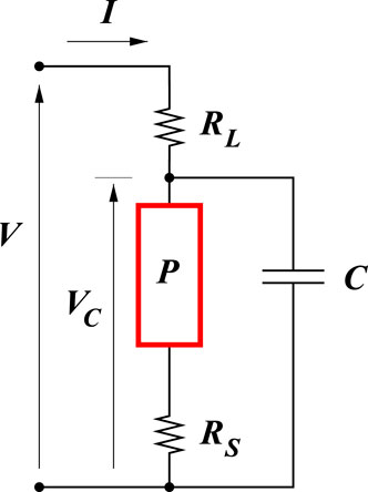
FIGURE 1. Circuit embedding the PCM [33]. Parameters referred to the PCM take suffix P in the equations and figures.
The inclusion of the circuit into the simulation can be done at different levels of completeness. The first, more general level (Section 2.4.1), couples the circuit with a numerical model of the Ovonic device; with respect to that illustrated in Section 2.1, 2.2, here the model is simplified by assuming that the device is homogeneous, while the dynamic aspects of the Ovonic device, as described by the relaxations times, are kept. The second level, less expensive from the numerical standpoint (Section 2.4.2), couples the external circuit with a static model of the Ovonic device, namely, a model of the form IP(VP).
To express the voltage drop VP across the Ovonic device, in the circuit model we assume a constant-field approximation, which is acceptable for devices longer than 10 nm [33]. It follows VP = L F(t), whence V = RL I + L F + A RS JP, with A the cross sectional area of the metallic plates and JP = q j the current density across the Ovonic device. Using Eq. 1 after neglecting the diffusive term yields a relation between the field and the mobile carrier concentration:
To complete the coupling with the external circuit, another equation is necessary; in it, the voltage drop VP must appear, which is in turn determined from the microscopic model accounting for the relaxation times. One notes from Figure 1 that
where the right hand side is prescribed. Eqs. 14 and 15 are then added to (6, 7, 9) to determine the electric performance of the OTS cell [33].
Still considering the circuit of Figure 1, a simpler analytical approach has been developed, which captures the key features of the voltage-dependent transient characteristic of OTS devices, and is suitable for implementation into device-simulation tools. The static characteristic of the PCM is sketched as shown in Figure 2; the approximation of considering a piecewise-linear characteristic has the advantage of affording an easy analytical approach2. Letting R1 (R2) be the resistance of the lower (upper) branch (R1 ≫ R2), it follows that the resistance of the series made of P and the heater is
with τL = RL C and
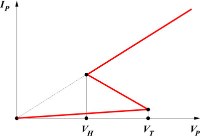
FIGURE 2. Schematic model of the S-shaped IP(VP) characteristic of the PCM.
As mentioned above, here the applied voltage is a ramp, V = α t, whence
In the first part of the ramp it is t0 = 0, VP < Vth, VC(t0) = 0, and
The voltage across P is related to VC by VC = VP (1 + RS/R1), and reaches the threshold value at a time tth such that
The VC(t) relation (19) is nonnegative and monotonic in the interval 0 ≤ t ≤ tth. When t reaches tth, the resistance of P changes abruptly, so that
In the second part of the ramp (t > tth) it is t0 = tth, VP > Vth, and
Here the equation to be solved has the same form as (16), with
The quantity to be measured is the current (V − VC)/RL provided by the bias, namely, using Eq. 19 for 0 ≤ t ≤ tth,
or, using Eq. 23 for t ≥ tth,
The asymptotic behavior of the current, obtained from Eq. 24 and 25 is, respectively,
The voltage pulse generated by experimental equipments varies from zero to its maximum programmed value in a finite time which, at present, can be as short as few ns [23,25]. Thus, every “real” voltage pulse contains, de facto, ramps with rise and fall times of finite duration; this implies the existence of a time transient of the electrical response of the device, during which the internal electric field increases or decreases. This effect may or may not be relevant according to how the rise time compares with the time scale of the microscopic processes responsible for the carrier heating at the origin of OTS, and whether or not the maximum voltage applied to the device exceeds the threshold voltage for the Ovonic switch. The simulations discussed in this section explore different physical situations of a GST-225 chalcogenide device, starting from ideal cases where circuit parasitic elements are absent and the external pulses have negligible rise times, then moving towards conditions closer to reality. The study is intended to test our theoretical model, based on hot-carrier effects, against experimentally-detected electric properties of amorphous chalcogenides, on time scales around and below the nanosecond, obtained from the last experimental results appeared in the literature [25]. In absence of information about the cross-sectional area of the devices employed in the experiments, the value 5, 000 nm2 has been used in all simulations to convert current densities obtained from the simulations into charge currents.
The exploration starts from the ideal case of negligible parasitic effects and negligible rise time of the applied voltage. Assuming a step-shaped voltage profile, the time dependence of the quantities relevant for transport is due only to the microscopic parameters of the model (such parameters are listed in Table 1). Some parameters are known from experiments, while others can be tuned on the basis of the details of the IP(VP) characteristic for a variety of bias conditions. A preliminary study about the influence of the microscopic parameters on the transport results obtained from the present model is reported in [34]; there, in particular, the microscopic parameter τT of Eq. 8 has been proven to control the heating process of the carriers for a given internal field and, consequently, the value of the threshold voltage. In the same paper, however, a discrepancy was found between the delay time td predicted by the model (of the order of tens of ps) and the much longer experimental values (possibly also influenced by parasitic effects).
TABLE 1. Microscopic parameters of Eqs. 6, 7, 9, 10. Apart from τn, the parameter values are taken from [34].
In a recent paper [25] for GST-225, the experimental steady-state OTS voltage (Vth) for a device of lenght L = 53 nm, obtained with very long leading/trailing edges of the applied voltage, is Vth = 2.0 ± 0.1 V. This value corresponds to a threshold field Eth ∼ 107 V/m, and compares well with that obtained in [34] for τT = 0.15 ps. Consequently, this value for τT is also used in the present paper. The electric measurements in the time domain also reported in [25] allow for a theoretical test on the second microscopic parameter τn of Eq. 7, which rules the relaxation of the mobile carrier population to the steady state value for a given applied field.
Based on the set of parameters of [34], a batch of simulations is presented here for different values of τn in order to assess the effect of this parameter on the rise time of the current after the application of a voltage step above threshold (here the value V = 2.4 V has been used for the voltage step). The results are reported in Figure 3; while no effect of the variation of τn has been found on the threshold value, it is seen that a delay time of about 1 ns (that is, in the same range of the experiments [25]) is achieved with τn = 0.6 ns, thus demonstrating that the theoretical model can be tuned in such a way as to compare well with experiments in the nanosecond scale.
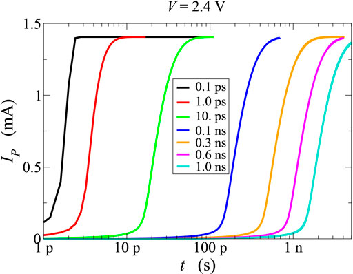
FIGURE 3. Current flowing across the PCM device as a function of time after the application of a 2.4 V external voltage step at t = 0. Different values for the microscopic parameter τn have been tested.
Furthermore, Figure 4 shows current IP as a function of time for different values of the step voltage: the higher the voltage, the shorter the delay time of the current, yielding a delay shorter than a ns at the largest biases considered. This behaviour is in agreement with experimental evidence [25].
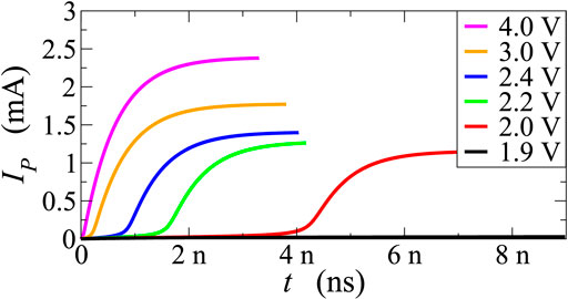
FIGURE 4. Current flowing across the PCM device as a function of time after the application of voltage steps of different amplitudes. The microscopic parameter τn has been set to 0.6 ns.
A step towards realistic bias conditions is achieved by considering that external waveform generators provide pulses with finite rise and fall times. Top-level equipments generate voltage pulses with rise and fall times as fast as 1 ns, and with 1.5 ns Full-Width Half Maximum (FWHM) [25]. These times are comparable with the microscopic relaxation times that govern the heating process and are assumed to be responsible for the OTS effect. Thus, still in absence of parasitic effects, a comparison of the theoretical predictions with the experimental scenario on a ns time scale has been carried on with reference to the bias conditions reported in [25].
Figure 5 reports the current flowing across the GST layer, as a function of time, due to the application of a trapezoidal profile with 1.5 ns rise and fall times, and a 4 ns duration of the plateau. Different values of the plateau have been considered, ranging from 2 V (corresponding to the OTS voltage) up to 4 V. Figures 6, 7 report similar data for 2.8 and 4 V plateau amplitudes, respectively, with plateau durations of 0, 2, and 4 ns in each case.
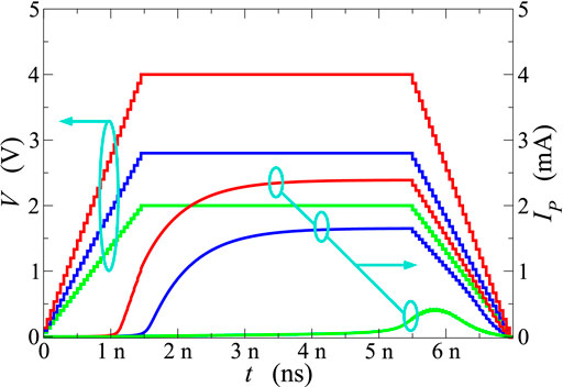
FIGURE 5. Current flowing across the PCM device as a function of time (right scale) after the application of voltage trapezoidal profiles of different amplitude (left scale). In all cases, rise and fall times are 1.5 ns and the duration of the plateau is 4 ns.
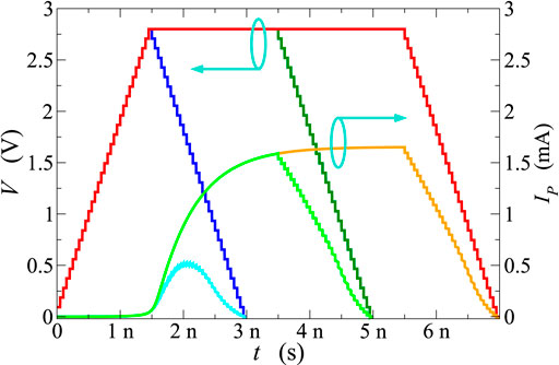
FIGURE 6. Current flowing across the PCM device as a function of time (right scale) after the application of voltage trapezoidal profiles of 2.8 V amplitude (left scale). Rise and fall times are 1.5 ns in all cases, whereas the plateau durations are 0, 2, and 4 ns.
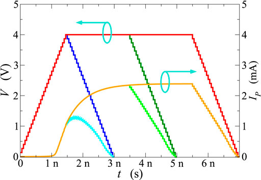
FIGURE 7. Current flowing across the PCM device as a function of time (right scale) after the application of voltage trapezoidal profiles of 4 V amplitude (left scale). Rise and fall times are 1.5 ns in all cases, whereas the plateau durations are 0, 2, and 4 ns.
In agreement with what reported by [25], ultrafast transient characteristics in the ns scale and below have been obtained in all considered cases. These results suggest that the delay time td, defined as the time elapsed between the instant at which the external bias exceeds the steady-state threshold value and the steep rise in the device current, varies in a wide range of values depending on the shape of the applied voltage. In particular, for plateau values significantly above threshold the carrier-heating process is very effective well before the maximum value of the voltage is reached; consequently, shorter delay times are observed (Figure 5). Moreover, when the plateau value and the rise and fall times are fixed, the duration of the plateau influences the maximum value of the measured current, but does not affect the delay time (Figures 6, 7).
All the above results are in agreement with those of [25], and confirm the validity of a theoretical model for the OTS process based on purely electronic mechanisms. At least in absence of parasitic effects, and provided that the microscopic time constants of the chalcogenide in hand lie in the ns range and below, the speed of threshold switching in OTS devices can be pushed below the ns scale by a voltage pulse of suitable duration and value. Figure 8 summarises the results for the delay time td as a function of the applied voltage amplitude for the bias conditions considered so far. For rise and fall times of 1.5 ns, the delay times obtained for the step (red symbols) and trapezoidal profiles (green symbols) are almost overlapping near threshold, while at higher biases the response to the trapezoidal shape exhibits still comparable, but longer delay times; this is probably due to a slower carrier heating process when the voltage ramps up the maximum value in about a ns. In all cases considered, the delay times obtained for applied voltages above 2.5 V are below the ns time scale.
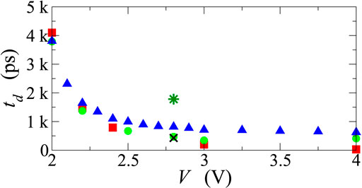
FIGURE 8. Simulated delay time td as a function of the amplitude of the applied signal V. The red squares and the green circles refer to the case where the input signal is applied directly to the PCM and consists of a voltage step or, respectively, of a trapezoidal voltage pulse like those of Figure 5 (in the latter case the amplitude of V is given by the plateau value). The blue triangles refer to the case where the input signal (still a trapezoidal pulse) is applied through the circuit of Figure 1, with RL = RS = 1 Ω and C = 300 pF. The cross (star) shows the delay time for V = 2.8 V when the value of the capacitance is changed to 30 pF or 1,000 pF, respectively.
Parasitic effects connected to the measuring system and wirings can be minimized with a top level apparatus, but cannot be eliminated in full. To account for their contribution we have repeated the simulations of the delay time after embedding the PCM device into the circuit of Figure 1, varying the equivalent capacitance C. The series resistances have been set at negligible values, since previous investigations pointed out a major modulating effect of the capacitance [33]. The characteristic time of the circuit is thus proportional to τL = RL C, and acts as an additional delay time.
Figure 9 reports the voltage drop Vp across the PCM when the input signal has a trapezoidal form, with 1.5 ns rise and fall times, and a 2.8 V plateau with a 2 ns duration; the equivalent capacitance has been varied from 30 to 2000 pF. Due to the broadening of VP (top panel), the higher the capacitance the shorter is the time interval during which VP > Vth. By way of example, C = 2000 pF corresponds to τL = 2 ns, equal to the duration of the plateau; in this case the electronic switching is hindered (low panel), because the switching to the ON state occurs only if the applied signal is kept at its plateau value long enough, in such a way that the electronic processes described earlier can be activated and completed. Similar results are also shown in Figures 10, 11, where the duration of the plateau is increased from 0 to 4 ns, while the capacitance is kept fixed. Once again, the maximum voltage drop Vp is always larger than the threshold voltage but, if the signal drops soon after reaching the maximum value, the threshold switching does not occur (low panel of Figure 10, black curve) or is incomplete (low panel of Figure 11, black curve). These results are consistent with the findings of [25]. The delay times of the current switch as functions of the plateau value of the external-voltage profile, for the cases considered in this section, are reported in Figure 8 (blue triangles, cross, and star), and compared with those obtained in absence of parasitic effects. As expected, capacitive effects produce longer delay times, and only with advanced experimental setups the delays can be reduced to values below the ns scale, as experimentally confirmed by [25].
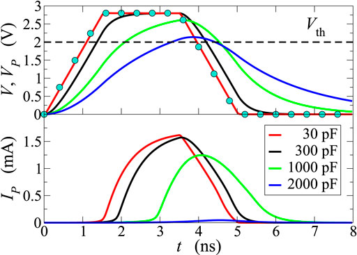
FIGURE 9. Simulated voltage drop VP (above) and current IP (below) of the PCM. The input signal V (above, circles) has a trapezoidal form with a plateau at 2.8 V, and is applied through the circuit of Figure 1 with RL = RS = 1 Ω. Capacitance C is given different values as shown in the figure. The horizontal, dashed line marks the threshold voltage Vth.
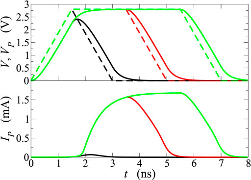
FIGURE 10. Same as in Figure 9, with different durations of the plateau of V; the latter is set at 2.8 V, and capacitance C is set at 300 pF.
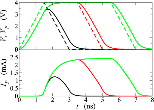
FIGURE 11. Same as in Figure 10, with different durations of the plateau of V; here the latter is set at 4 V, and capacitance C is kept 300 pF.
For the sake of completeness we point out that the present transport model was developed for the amorphous OFF phase, and its parameters have been optimised for describing the subthreshold region. ON state currents are underestimated, and a quantitative comparison with the experimental currents also in the amorphous ON region preceeding the phase change would require a further model enhancement like, e.g., the inclusion of electron band states and the mobility increase that sets in when electrons coming from low-mobility states are excited to high-energy mobile states, and a consequent parameter recalibration. However, an even steeper rise of the current is expected not to alter appreciably the present findings.
In conclusion, we can split the measured delay time into two components: the former one is intrinsic to the switching phenomenon, and is associated to the time required to promote a significant number of carriers from localized to mobile states, thanks to carrier heating induced by the electric field (a similar change in the transport mechanism is also proposed in [37]); the latter component is instead depending on the measuring apparatus and wirings, and acts as a nearly rigid offset. This component can largely dominate if no particular care is taken in designing the circuitry. To support this statement, we see in Figure 8 that increasing the capacitance by about three times nearly doubles the delay time.
A simplified analysis of the same issue has been carried out for comparison, with reference to the circuit of Figure 1, and to the schematic model of the PCM characteristic of Figure 2. The delay time td has been calculated from the relations of Section 2.4.2, using the same values of the lumped elements as those of Figure 8. The S-shaped IP(VP) characteristic of the PCM has been modeled with R1 = 1 MΩ and R2 = 1 kΩ, a threshold voltage Vth = 2 V, and a contact resistance RS = 1 Ω. It is worth observing that, since the PCM is described with a static characteristic, here the delay is due to the combined effect of RL and C (in other terms, there would be no delay if RL = 0 and/or C = 0). The ramp slope α = 1.87 × 10⁹ V/s (α = 2.67 × 10⁹ V/s) corresponds to a rise time of 1.5 ns from V = 0 to V = 2.8 V (V = 4 V); it follows that V = α t becomes equal to the threshold voltage at t′ ≃ 1.07 ns (t′ = 0.75 ns).
The results are summarized in Table 2; one notes that, as expected, the same value of τL = RL C provides the same value of td. Comparing with Figure 8, one also notes that the delay times calculated as in Section 2.4.2 are lower (by a factor 2.5 at least) than those shown in Figure 8. Remembering the discussion carried out in the first part of this section, this outcome is ascribed to the fact that, as the PCM characteristic of Figure 2 is purely static, the expressions of Section 2.4.2 do not account for the additional delay due to the internal relaxation times of the PCM.
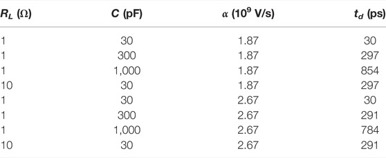
TABLE 2. Delay time td as a function of the lumped elements of Figure 1. Symbol α indicates the slope of the ramp (see text).
The delay time of the OTS onset, i.e., the delay between the instant at which the external voltage applied to the chalcogenide cell equals the static threshold voltage and the instant at which a steep rise of the current through the OTS device occurs, is a quantity that is strongly influenced by the time dependence of the applied voltage. This effect has been studied in this paper by means of theoretical approaches of different complexities, all based upon the assumption that OTS is mainly due to electronic effects.
A purely microscopic model based on a trap-limited transport scheme with appropriate microscopic parameters provides delay times below the ns limit, as recently measured in GST-225 cells [25]. The availability of new experimental results for this chalcogenide in the ns–ps time domain allows for a better tuning of the microscopic parameter τn, which greatly improves the theoretical quantitative results for the delay time with respect to our previous work [30,34]. Parasitic effects do not produce a noticeable increase of td, at least for suitably optimised, electrical-test systems like those used in advanced experiments. Based on the simulation tests performed with detailed microscopic models, an analytical, computationally efficient approach has been developed which captures the key features of the voltage-dependent transient characteristic of OTS devices, and is suitable for implementation into device-simulation tools.
The simulated transient currents are in substantial agreement with the experimental values obtained with similar external bias voltages, this confirming the existence of delay times in the sub-ns time scale on the basis of the physical process of carrier heating due to energy transfer from the external field. Analytical calculations confirm that, for realistic values of the parasitic parameters, the internal relaxation times of the PCM provide a non-negligible contribution to the delay time td.
The datasets presented in this article are not readily available because intellectual property of the University of Bologna and University of Modena and Reggio Emilia. Requests to access the datasets should be directed to cm9zc2VsbGEuYnJ1bmV0dGlAdW5pbW9yZS5pdA==.
All authors listed have made a substantial, direct, and intellectual contribution to the work and approved it for publication.
Author EP was employed by Applied Materials Italia s.r.l.
The remaining authors declare that the research was conducted in the absence of any commercial or financial relationships that could be construed as a potential conflict of interest.
All claims expressed in this article are solely those of the authors and do not necessarily represent those of their affiliated organizations, or those of the publisher, the editors, and the reviewers. Any product that may be evaluated in this article, or claim that may be made by its manufacturer, is not guaranteed or endorsed by the publisher.
The Authors gratefully acknowledge useful discussions with Prof. Anbarasu Manivannan and his team members.
1Elsewhere the Poole-Frenkel model, viz,
2In principle, the approximation of a piecewise-linear characteristic could be avoided: one may in fact invert VC = VP + RS IP(VP) to extract IP(VC), then solve
1. Servalli G. A 45nm Generation Phase Change Memory Technology. In: IEEE International Electron Devices Meeting (IEDM), Technical Digest (2009). p. 1–4. doi:10.1109/iedm.2009.5424409
2. Burr GW, Shenoy RS, Virwani K, Narayanan P, Padilla A, Kurdi B, et al. Access Devices for 3D Crosspoint Memory. J Vacuum Sci Technol B, Nanotechnology Microelectronics: Mater Process Meas Phenomena (2014) 32:040802. doi:10.1116/1.4889999
3.[Dataset] Optane. Intel 3D XPoint Memory Die Removed from Intel Optane™ PCM (Phase Change Memory) (2017). Available from: http://techinsights.com/about-techinsights/overview/blog/intel-3D-xpoint-memory-die-removed-from-intel-optane-pcm/ (Accessed March 15, 2018)
4.[Dataset] Optane. Memory/Selector Elements for Intel Optane™ XPoint Memory (2017). Available from: http://techinsights.com/about-techinsights/overview/blog/memory-selector-elements-for-intel-optane-xpoint-memory/ (Accessed March 15, 2018)
5.[Dataset] Choe J. Memory/Selector Elements for Intel OptaneTM XPoint Memory (2017). Available from: http://techinsights.com/ (Accessed March 15, 2018)
6. Arnaud F, Zuliani P, Reynard J, Gandolfo A, Disegni F, Mattavelli P, et al. Truly Innovative 28nm FDSOI Technology for Automotive Micro-controller Applications Embedding 16MB Phase Change Memory. In: IEEE International Electron Devices Meeting (IEDM), Technical Digest (2018). p. 18.4.1–18.4.4. doi:10.1109/iedm.2018.8614595
7. Markram H, Gerstner W, Sjöström PJ. A History of Spike-timing-dependent Plasticity. Front Syn Neurosci (2011) 3:4. doi:10.3389/fnsyn.2011.00004
8. Le Gallo M, Sebastian A, Mathis R, Manica M, Giefers H, Tuma T, et al. Mixed-precision In-Memory Computing. Nat Electron (2018) 1:246–53. doi:10.1038/s41928-018-0054-8
9. Sebastian A, Le Gallo M, Khaddam-Aljameh R, Eleftheriou E. Memory Devices and Applications for In-Memory Computing. Nat Nanotechnol (2020) 15:529–44. doi:10.1038/s41565-020-0655-z
10.[Dataset] Sarwat SG, Kersting B, Moraitis T, Jonnalagadda VP, Sebastian A. Phase Change Memtransistive Synapse (2021).
11. Lai S. Current Status of the Phase Change Memory and its Future. In: IEEE International Electron Devices Meeting (IEDM), Technical Digest (2003). p. 10.1.1–10.1.4.
12. Raoux S, Wuttig M. Phase Change Material — Science and Applications. Berlin, Germany: Springer (2009).
13. Kolobov AV, Tominaga J. Chalcogenides — Metastability and Phase Change Phenomena. Materials Science. Berlin, Germany: Springer (2012).
15. Loke D, Lee TH, Wang WJ, Shi LP, Zhao R, Yeo YC, et al. Breaking the Speed Limits of Phase-Change Memory. Science (2012) 336:1566–9. doi:10.1126/science.1221561
16. Anbarasu M, Wimmer M, Bruns G, Salinga M, Wuttig M. Nanosecond Threshold Switching of GeTe6 Cells and Their Potential as Selector Devices. Appl Phys Lett (2012) 100:143505. doi:10.1063/1.3700743
17. Rao F, Ding K, Zhou Y, Zheng Y, Xia M, Lv S, et al. Reducing the Stochasticity of crystal Nucleation to Enable Subnanosecond Memory Writing. Science (2017) 358:1423–7. doi:10.1126/science.aao3212
18. Mott NF, Davis EA. Electronic Processes in Non-crystalline Materials. Oxford: Clarendon Press (1971).
19. Li H, Robertson J. Materials Selection and Mechanism of Non-linear Conduction in Chalcogenide Selector Devices. Sci Rep (2019) 9:1867. doi:10.1038/s41598-018-37717-x1
20. Raty J-Y, Noé P. Ovonic Threshold Switching in Se‐Rich Ge X Se 1− X Glasses from an Atomistic Point of View: The Crucial Role of the Metavalent Bonding Mechanism. Phys Status Solidi RRL (2020) 14(1–7):1900581. doi:10.1002/pssr.201900581
21. Clima S, Garbin D, Opsomer K, Avasarala NS, Devulder W, Shlyakhov I, et al. Ovonic Threshold‐Switching Ge X Se Y Chalcogenide Materials: Stoichiometry, Trap Nature, and Material Relaxation from First Principles. Phys Status Solidi RRL (2020) 14:1900672. doi:10.1002/pssr.201900672
22. Noé P, Verdy A, d’Acapito F, Dory J, Bernard M, Navarro G, et al. Toward Ultimate Nonvolatile Resistive Memories: The Mechanism behind Ovonic Threshold Switching Revealed. Sci Adv — Mater Sci (2020) 6:1–10. Available from: https://www.science.org (Accessed July 30, 2021).
23. Wimmer M, Salinga M. The Gradual Nature of Threshold Switching. New J Phys (2014) 16:113044. doi:10.1088/1367-2630/16/11/113044
24. Shukla KD, Saxena N, Durai S, Manivannan A. Redefining the Speed Limit of Phase Change Memory Revealed by Time-Resolved Steep Threshold-Switching Dynamics of AgInSbTe Devices. Sci Rep (2016) 6:37868. doi:10.1038/srep37868
25. Saxena N, Raghunathan R, Manivannan A. A Scheme for Enabling the Ultimate Speed of Threshold Switching in Phase Change Memory Devices. Sci Rep (2021) 11:6111. doi:10.1038/s41598-021-85690-9
26. Shukla KD, Saxena N, Manivannan A. An Ultrafast Programmable Electrical Tester for Enabling Time-Resolved, Sub-nanosecond Switching Dynamics and Programming of Nanoscale Memory Devices. Rev Scientific Instr (2017) 88:123906. doi:10.1063/1.4999522
27. Ielmini D. Threshold Switching Mechanism by High-Field Energy Gain in the Hopping Transport of Chalcogenide Glasses. Phys Rev B (2008) 78:035308. doi:10.1103/physrevb.78.035308
28. Cappelli A, Piccinini E, Xiong F, Behnam A, Brunetti R, Rudan M, et al. Conductive Preferential Paths of Hot Carriers in Amorphous Phase-Change Materials. Appl Phys Lett (2013) 103:083503. doi:10.1063/1.4819097
29. Buscemi F, Piccinini E, Cappelli A, Brunetti R, Rudan M, Jacoboni C. Electrical Bistability in Amorphous Semiconductors: A Basic Analytical Theory. Appl Phys Lett (2014) 104:022101. doi:10.1063/1.4861658
30. Brunetti R, Jacoboni C, Piccinini E, Rudan M. Band Transport and Localised States in Modelling the Electric Switching of Chalcogenide Materials. J Comput Electron (2020) 19:128–36. doi:10.1007/s10825-019-01415-2
31. Bogoslovskij NA, Tsendin KD. Electronic-thermal Switching and Memory in Chalcogenide Glassy Semiconductors. J Non-Crystalline Sol (2011) 357:992–5. doi:10.1016/j.jnoncrysol.2010.11.048
32. Le Gallo M, Athmanathan A, Krebs D, Sebastian A. Evidence for Thermally Assisted Threshold Switching Behavior in Nanoscale Phase-Change Memory Cells. J Appl Phys (2016) 119:025704. doi:10.1063/1.4938532
33. Piccinini E, Brunetti R, Bordone P, Rudan M, Jacoboni C. Transient and Oscillating Response of Ovonic Devices for High-Speed Electronics. J Phys D: Appl Phys (2016) 49:495101. doi:10.1088/0022-3727/49/49/495101
34. Jacoboni C, Piccinini E, Brunetti R, Rudan M. Time- and Space-dependent Electric Response of Ovonic Devices. J Phys D: Appl Phys (2017) 50:255103. doi:10.1088/1361-6463/aa71e5
35. Poole HH. VIII. On the Dielectric Constant and Electrical Conductivity of Mica in Intense fields. Lond Edinb Dublin Philos Mag J Sci (1916) 32:112–29. Ser. 6. doi:10.1080/14786441608635546
36. Press WH, Flannery BR, Teukolsky SA, Wetterling WT. Numerical Recipes — the Art of Scientific Computing. New York: Cambridge University Press (1988).
37. Noé P, Vallée C, Hippert F, Fillot F, Raty JY. Phase-change Materials for Non-volatile Memory Devices: from Technological Challenges to Materials Science Issues. Semicond Sci Technol (2017) 33:013002.
Keywords: chalcogenides, GST, ovonic threshold switching, phase change memories, charge transport, amorphous materials
Citation: Brunetti R, Jacoboni C, Piccinini E and Rudan M (2022) Time-Domain Analysis of Chalcogenide Threshold Switching: From ns to ps Scale. Front. Phys. 10:854393. doi: 10.3389/fphy.2022.854393
Received: 13 January 2022; Accepted: 04 March 2022;
Published: 06 April 2022.
Edited by:
Francesco Caravelli, Los Alamos National Laboratory (DOE), United StatesReviewed by:
Huanglong Li, Tsinghua University, ChinaCopyright © 2022 Brunetti, Jacoboni, Piccinini and Rudan. This is an open-access article distributed under the terms of the Creative Commons Attribution License (CC BY). The use, distribution or reproduction in other forums is permitted, provided the original author(s) and the copyright owner(s) are credited and that the original publication in this journal is cited, in accordance with accepted academic practice. No use, distribution or reproduction is permitted which does not comply with these terms.
*Correspondence: R. Brunetti, cm9zc2VsbGEuYnJ1bmV0dGlAdW5pbW9yZS5pdA==
Disclaimer: All claims expressed in this article are solely those of the authors and do not necessarily represent those of their affiliated organizations, or those of the publisher, the editors and the reviewers. Any product that may be evaluated in this article or claim that may be made by its manufacturer is not guaranteed or endorsed by the publisher.
Research integrity at Frontiers
Learn more about the work of our research integrity team to safeguard the quality of each article we publish.