 Wenhui Wan
 Na Kang
 Yong Liu
95% of researchers rate our articles as excellent or good
Learn more about the work of our research integrity team to safeguard the quality of each article we publish.
Find out more
ORIGINAL RESEARCH article
Front. Phys. , 11 March 2022
Sec. Condensed Matter Physics
Volume 10 - 2022 | https://doi.org/10.3389/fphy.2022.843352
This article is part of the Research Topic Spintronic Materials and Devices View all 6 articles
In this study, the structural and magnetic properties of Si-doped bulk and 2D AlN were systematically investigated by first-principles calculations. Si atoms prefer to substitute Al atoms in both bulk and 2D AlN under N-rich growth conditions. In bulk AlN, Si dopants exhibit a non-magnetic state, uniform distribution, and a strong anisotropic diffusion energy barrier. In contrast to that, Si dopants prefer to form a buckling structure and exhibit a magnetic moment of 1 μB in 2D AlN. At a low Si concentration, Si atoms tend to get together with antiferromagnetic coupling between each other. However, the magnetic coupling among Si atoms changes to ferromagnetic coupling as Si concentration increases, due to the enhanced exchange splitting and delocalized impurity states. At the extreme doping limit, monolayer SiN, along with its analogs GeN and SnN, is a ferromagnetic semiconductor with a large band gap and high Curie temperature. These results indicate that 2D AlN doped by group IV atoms has potential applications in spintronic devices.
Bridging semiconductor and magnetism is desirable to utilize charge and spin degrees of freedom simultaneously, thereby creating enhanced functionalities beyond conventional semiconductor devices [1, 2]. Diluted magnetic semiconductors (DMSs) have been realized by doping group III-V and II-VI compounds with a few percent of transition metal (TM) ions, whose magnetism arises from the ferromagnetic (FM) coupling between the electrons in the partially filled d or f orbitals [3, 4]. However, some nanomaterials without d or f electrons also exhibit magnetic behavior, which is called d0 magnetism [5]. That unexpected magnetism arises from the increase in the Coulomb interactions/bandwidth ratio induced by the reduction of materials’ dimensions [6]. At present, d0 magnetism is a fast-growing field and calls for important material developments [7].
Bulk aluminum nitride (AlN) in the wurtzite structure has a wide direct gap, a high breakdown field, and a high thermal conductivity [8]. In 2013, monolayer AlN with a hexagonal lattice was synthesized on single-crystal Ag (111) by plasma-assisted molecular beam epitaxy [9]. The band gap of 2D AlN can be modulated by in-plane strain or a transverse electric field [10]. Both bulk and 2D AlN have promising applications in optics, spintronics, optoelectronics, and as substrate materials [11]. In the past decades, room-temperature (RT) ferromagnetism in wurtzite AlN-based DMSs [12] has been recognized by doping transition metal (TM) dopants such as Mn [13], Cr [14], V [15], Fe [16], Co [17], Ni [18], Cu [19, 20], Zn [21], Ti [22], Ce [23], and Ag [24]. The unpaired d orbitals of TM dopants dominate the magnetic moment in AlN-based DMSs. The FM coupling between TM ions was explained by various models including double exchange [13–15, 22], superexchange exchange [23], p–d hybridization [16, 20, 24], and bound magnetic polaron models [18, 19, 21]. Besides TM ions, wurtzite AlN doped by alkali metals [25], Mg [26], and Ga [27] atoms also exhibit ferromagnetism, which was explained by the p–p hybridization interaction involving holes. In 2012, D. Pan et al reported the RT ferromagnetism in Si-doped wurtzite AlN films at a doping concentration of 0 ∼11% [28]. But that ferromagnetism was explained by the N vacancies, rather than external Si dopants [28].
On the other hand, monolayer AlN doped by TM atoms [29] and 1A or 2A main-group elements [30, 31] were also reported to have RT ferromagnetism. In previous research, silicon atoms can induce magnetic moments in monolayer AlN by surface adsorption [32], while the substituted Si will transfer to a non-magnetic (NM) state [32, 33]. However, Gupta et al. predicted that substituted Si could exhibit a magnetic moment in monolayer BN, which has a lattice structure similar to monolayer AlN [34]. Thus, the electronic and magnetic properties of Si dopants in both bulk and 2D AlN call for a comprehensive understanding due to a lack of relevant experiments. Both Si and AlN consist of earth-abundant elements and play a significant role in the semiconductor industry. Understanding the properties of the Si-doped AlN help expand their application prospect.
In this work, the preferred occupation, magnetic configuration, and diffusion of Si atoms in bulk and 2D AlN were investigated by first-principles calculations. We reveal that Si atoms tend to behave as NM-substituted dopants and distributed uniformly at low concentrations in bulk AlN. The easy diffusion direction of Si in bulk AlN is vertical to the (0001) crystal orientation. On the other hand, Si atoms prefer to substitute the Al atoms in a buckling structure with a magnetic moment in 2D AlN. The magnetic coupling between Si atoms changes from antiferromagnetic (AFM) to FM as the Si content increases. At the full Si substitution, monolayer SiN and its analogs GeN and SnN are 2D FM semiconductors.
All the first-principles calculations were performed by the Vienna ab initio simulation package (VASP) [35, 36] with the projector augmented wave (PAW) [37] pseudopotentials and Perdew–Burke–Ernzerhof (PBE) [38] exchange-correlation functionals. The kinetic energy cutoff was set at 450 eV. The Brillouin zone integrations are performed with 6 × 6 × 4 and 9, ×, 9 × 1 Monkhorst–Pack k points mesh [39] for bulk and monolayer AlN, respectively. The crystal structure and atomic position are fully optimized with a force convergence threshold of 0.01 eV/Å. The band gap was modified by using Heyd–Scuseria–Ernzerhof (HSE) functionals [40].
The formation energy Ef is defined as follows:
where EAlN and ESi+AlN are the total energy of intrinsic and Si-doped AlN, respectively; μAl and μN are the chemical potentials of the Al and N elements, respectively; and n is the negative or positive integer that represents the number of the removed or added atoms, respectively. In Al-rich growth conditions, μAl is equal to μAl [bulk], that is, energy per Al atom in face-centered Al substance. Meanwhile, μN is obtained by μN = μAlN − μAl [bulk], where μAlN is the energy per formula of AlN in bulk or monolayer AlN. Similarly, μN equals the energy per N atom in nitrogen molecules, and μAl = μAlN − μN [N2] in N-rich conditions. It is noted that the different growth conditions will affect the Ef of substituted Si rather than interstitial Si because nAl and nN in Eq. 1 are zero in the latter case.
The magnetic materials can be described by the Heisenberg Hamiltonian:
We considered interaction constants Jij up to third nearest neighbors. We determined the Jij through the relations between energy and spin configuration. Based on the Heisenberg Hamiltonian, the Monte Carlo (MC) simulations were performed by code MCsolver [41]. A 32 × 32 × 1 supercell is to estimate the Curie temperature Tc. We ran 105 MC sweeps to reach the thermal equilibrium state, followed by 2 × 10⁵ MC sweeps for the averaging of magnetizations and energies.
First, we obtained lattice constants a = 3.129 Å, c = 5.125 Å for bulk AlN, and a = 3.125 Å for monolayer, which are consistent with previous results [30, 31, 42].
We considered the doping of Si in bulk AlN. We placed a single Si atom into a large supercell with 288 atoms to simulate a dilute doping scenario in which the Si atom can be regarded as an isolated impurity (Figures 1A,B). We examined non-equivalent Si doping sites including the substitution of an Al atom (SiAl) or a N atom (SiN), the interstitial site with z coordination between two Al [labeled as SiI,Al by Kroger–Vink notation] layers or N (SiI,N) layers (Figure 2A). Frenkel defects (SiAl − AlI and SiN − NI) in which a Si atom occupies the Al or N site and repels the original Al or N atom to an adjacent interstitial site were also considered. We calculated the formation energies (Ef) of these doping configurations under Al- and N-rich growth conditions. The growth conditions will affect the Ef of substituted Si, rather than interstitial Si. Both non-magnetic and magnetic states of the Si atom were considered.
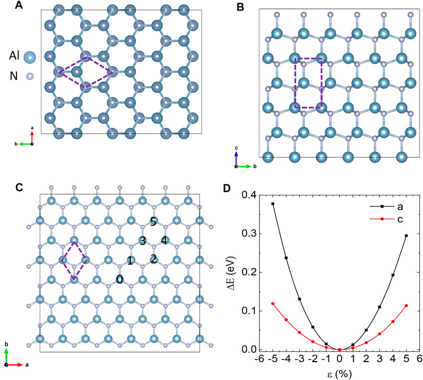
FIGURE 1. (A,B) Side views of bulk AlN along with the c and a axis. The primitive cell is labeled by dash lines. (C) Top view of monolayer AlN. A Si atom locates at 0 site and the other one can be at 1 ∼ 5 site. (D) The black and red lines represent the energy of the primitive cell of bulk AlN under strain along and vertical to the (0001) direction (the c axis), respectively. The energy of strain-free AlN was set to zero.
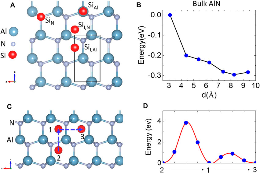
FIGURE 2. (A) Substituted SiAl and SiN sites; interstitial IAl and IN sites in bulk AlN. The sky blue, gray, and red balls represent Al, N, and Si atoms, respectively. (B) Total energy of Si-doped bulk AlN as a function of Si–Si separation. (C) The diffusion pathway of Si in bulk AlN. (D) Energy profile for a Si dopant diffusing parallel and vertical to the c axis.
The results of Ef are shown in Table 1. Si atoms at the SiI,N site are not stable and transfer to the SiI,Al site. In bulk AlN, Si atoms prefer to substitute Al atoms (SiAl), due to that the atomic radius and electronegativity of Si atoms are more close to those of Al atoms than N atoms. The ground magnetic state of SiAl is an NM state. The Ef of SiAl is smaller under N-rich than under Al-rich growth conditions, which is consistent with the experiment that Si incorporation in AlN films is suppressed under Al-rich growth conditions [43]. The magnetic state of the SiAl site is not stable and will transition to the NM state. We further calculated the density of states (DOS), which indicates that the SiAl site gives an impurity band very close to the conduction band, similar to the behavior of Si dopants in GaN [44]. Thus, the SiAl site is non-magnetic in bulk AlN because the unpaired electron is quite delocalized. Instead, the metastable SiN configuration prefers a magnetic state, with a magnetic moment of 1 μB. If enough N-vacancies exist in wurtzite AlN [45], external Si dopants can form SiN configurations and exhibit magnetism in bulk AlN, consistent with Pan’s experiment [28].
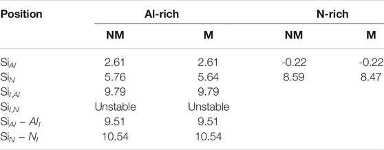
TABLE 1. Formation energies Ef (eV) of single Si atom in bulk AlN in the magnetic (M) and non-magnetic (NM) states under Al- or N-rich growth conditions.
The diffusion of Si atoms in bulk AlN can proceed through the interstitial SiI,Al site. As bulk AlN has an anisotropic lattice, we considered Si diffusion along the pathway parallel (2 → 1) and vertical (1 → 3) to the [0001] direction, which was labeled as the c axis (Figure 2C). We estimated the diffusion barrier ΔE using the nudged elastic band (NEB) method [46]. The Si element has a larger ionic radius than Ga and N elements, so Si ions will extrude Al and N ions along the direction vertical to the diffusion pathway. We found that the energy of the unit cell of AlN increases more slowly under strain parallel to the c axis than strain vertical to the c axis (Figure 1D). Thus, the ΔE of path 1 → 3 is smaller than the ΔE of path 2 → 1 (Figure 2D) due to the smaller energy needed to extrude Al and N atoms. Thus, Si atoms prefer to diffuse vertical to the c axis in bulk AlN.
We introduced two SiAl defects into the AlN supercell. The magnetic coupling between them can be NM, FM, or AFM. The total energy of AlN with two SiAl defects is presented in Figure 2B. Both FM and AFM states will transition into NM states. The energy of AlN with two NM SiAl defects decreases as the Si separation increases. Thus, Si atoms tend to act as NM dopants, distributed uniformly and diffuse vertically to the c axis in bulk AlN. That is consistent with experiments showing that Si incorporation in AlN is homogeneous under N-rich conditions [28, 43].
Next, we investigated the Si doping in 2D AlN. We put a single Si in a 6 × 6 × 1 supercell of monolayer AlN. We considered the substituted SiAl and SiN in buckling and planar structures, the adsorption of Si atoms on top of Al (SiT,Al), N atoms (SiT,N), hexagonal site (SiH), and bridge site (SiB) (Figure 3A). As shown in Table 2, the Si atom at the (SiB) site is not stable and will transfer to the SiT,N site. If we consider the Si in the NM state, the buckling SiAl structure is not stable will transition to the planar SiAl structure. We calculated the energy of SiAl configuration at different buckling heights in the NM state while keeping all atoms fixed. The energy profile in Figure 3B shows that the NM SiAl in the planar structure has the lowest energy.
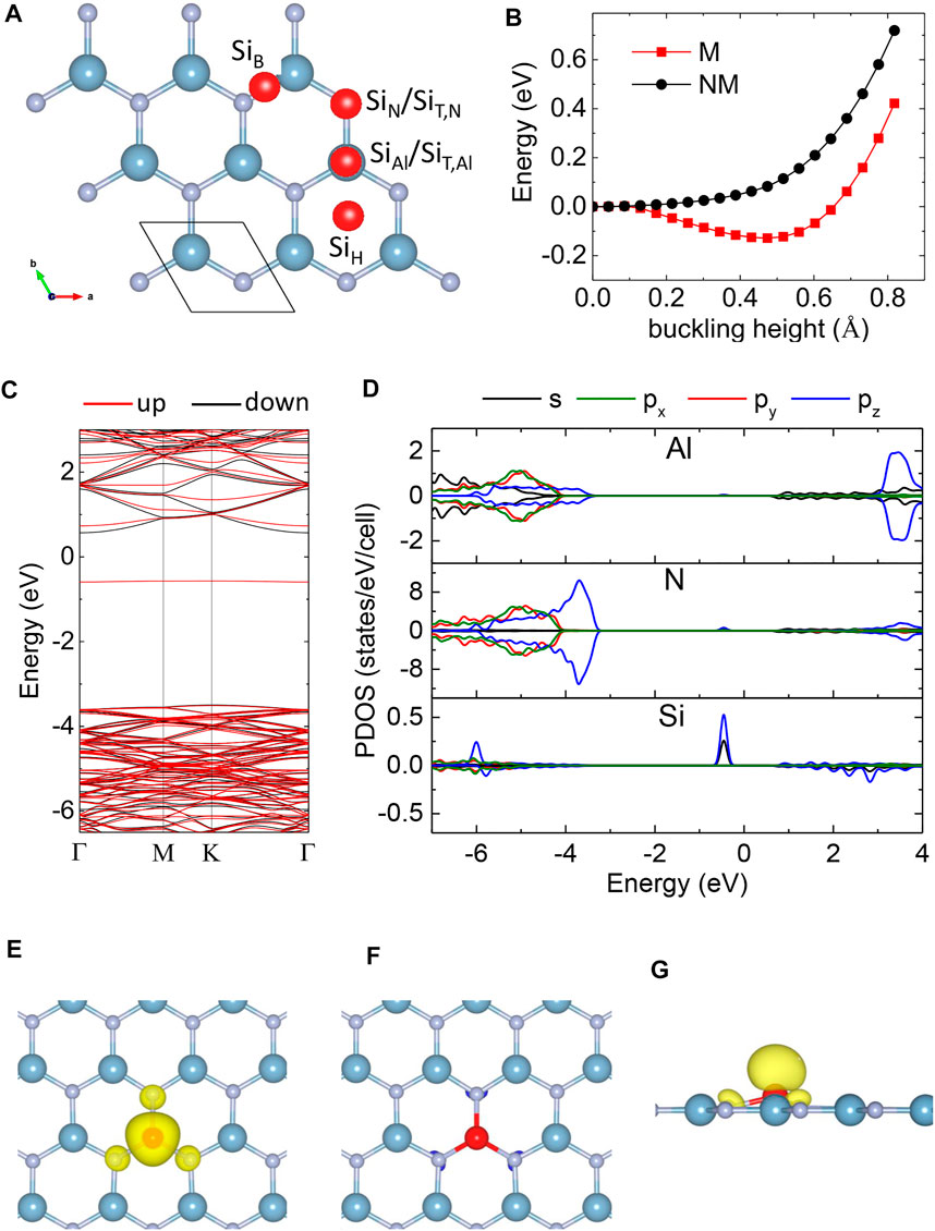
FIGURE 3. (A) Substituted SiAl and SiN; the adsorptional TAl, TN, B, and H sites in monolayer AlN. (B) The energy of SiAl structure in magnetic (M) and non-magnetic (NM) states as a function of the buckling height. The energy of planar structure was set to zero. (C) Band structure and (D) projected density of states of buckling SiAl structure. (E,F) The positive and negative spin densities of single-Si-doped monolayer AlN from the top view. (G) The same spin density from the side view. The isosurface of spin density is = 0.005 eV/Å3.
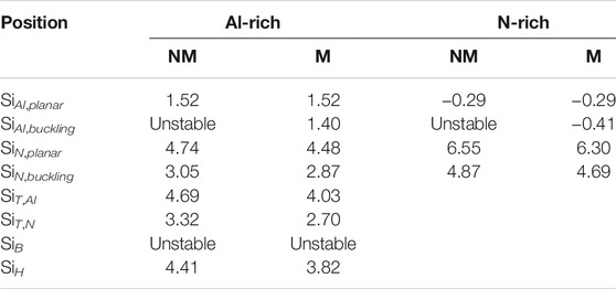
TABLE 2. Formation energies Ef (eV) of single Si atom in monolayer AlN in the magnetic (M) and non-magnetic (NM) states under Al- or N-rich growth conditions.
However, if we consider Si in a spin-polarized state, the buckling SiAl structure becomes the most stable doping configuration (Table 2; Figure 3B). The optimized Si–N bond lengths are 1.697 Å and 1.749 Å in the plane and buckling SiAl structures, respectively. As the ionic radius of the Si dopant is larger than that of the Al ion in Si-doped 2D AlN, the Si dopant prefers a buckling structure to release the strain and make the system energetically lower. That is similar to alkali metals which also form buckling SiAl structures in monolayer AlN [47]. The stable SiAl structure has a buckling height of 0.49 Å and a magnetic moment of 1 μB per Si atom.
SiN and other adsorption configurations, which can induce a magnetic moment of 1 or 2 μB per Si atom, have much higher Ef (Table 2). Thus, the Si atom prefers to substitute the Al atom with a non-zero magnetic moment in the monolayer AlN.
Based on the HSE06 hybrid functional [40], the band structure and partial density of states (PDOS) of single-Si-doped monolayer AlN are displayed in Figures 3C, D. A diluted Si-doped AlN is still a semiconductor. The pristine AlN monolayer has D3h symmetry, and the 2p states of the N atom split into a singlet pz state and doubly degenerate states px and py with lower energy. The induced Si dopants in the SiAl site deform the D3h symmetry of the AlN lattice, resulting in small splitting between px and py states (Figure 3D). The PDOS of the Si-p and N-p orbitals overlapped at an energy of around −6 eV in the deep valence band (Figure 3D). The Si atom contributes three valence electrons to participate in the bonding with neighboring N-p orbitals, lifting an unpaired electron to form a dispersion-less impurity band in the spin-up channel within the band gap (Figure 3C). The asymmetric PDOS creates a magnetic moment of 1 μB per Si atom. Si-pz and Si-s orbitals dominate the electronic states of the impurity band. The impurity band is a deep donor level, which is consistent with the n-type conductivity of Si-doped AlN in the experiment [28].
The spin density of SiAl structures is displayed in Figures 3E,F. The negative spin density is insignificant compared to the positive spin density (Figure 3F). Spin density exhibits localization at the Si site. The nearest N neighbors around the Si dopant had a small contribution to the magnetic moment and exhibited an FM coupling with the Si dopant (Figure 3E). The Al atoms display virtually no spin polarization. We can conclude that the additional charge carriers due to Si doping promote ferromagnetism in monolayer AlN. The situation is similar to that of Cr-doped AlN nanowires with the ferromagnetic coupling of the Cr atoms [48].
We further decomposed magnetic moment origin. The p orbitals of Si dopants and the nearest-neighboring N atoms dominate the magnetic moments. The Si-s orbital and nearest-neighboring N-s orbital have a small contribution to the magnetic moments. That is different from Mg- or Ga-doped monolayer AlN where spin-polarized 2p orbitals of N neighbors around dopants dominate the magnetic moment [26, 27].
The diffusion of Si atoms in monolayer AlN can proceed along the direction vertical to or parallel to the AlN sheet. The former one can proceed between two equivalent SiAl sites on the different sides of the AlN sheet (Figure 4A). We performed NEB calculations and allowed the atomic positions to be relaxed. The diffusion barrier △E is estimated at 0.11 eV (Figure 4B). The accurate energy profile of Si diffusion indicates that the planar SiAl configuration is a metastable state (Figure 4B). If the initial buckling height was set to be small in the simulation of structure relaxation, one may finally predict a planar SiAl configuration in spin-polarized calculations. That may be the reason for the difference between our results and previous work [32, 33]. The other diffusion pattern is through low-energy adsorption sites on the same side of the AlN sheet, which is SiT,N − SiH − SiT,N pathway (Figure 4C). Through the NEB calculations, the optimized saddle point was still close to the H site. The diffusion barrier △E was estimated at 1.11 eV (Figure 4D), which is much larger than △E crossing the AlN sheet.
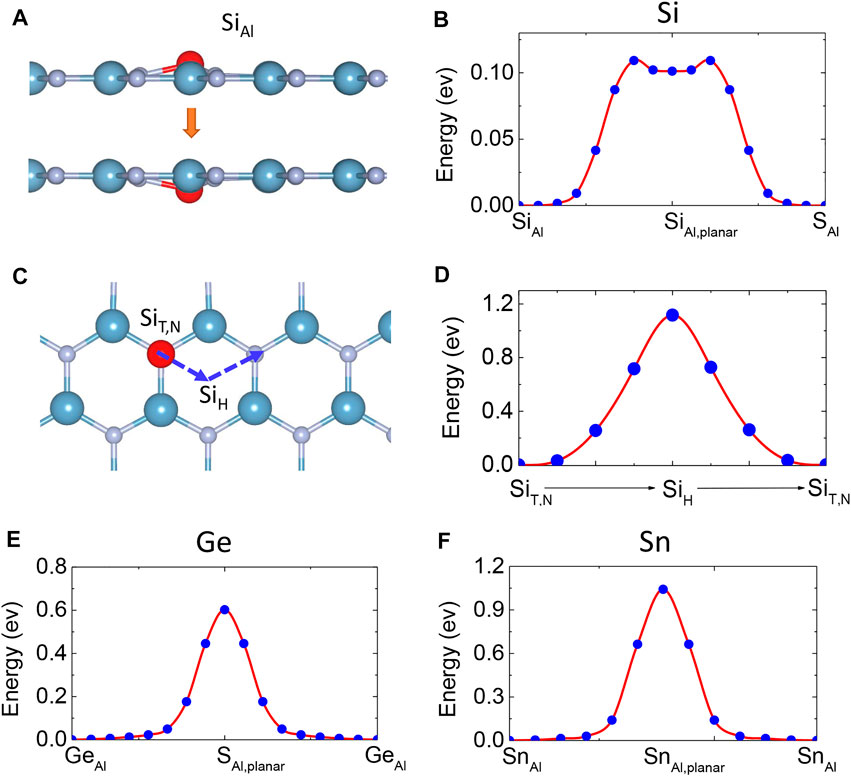
FIGURE 4. (A) Diffusion pathway of Si passing through the monolayer AlN. (B) Energy profiles for the diffusion path of Si. (C) Pathway and (D) energy profile of a Si dopant diffusing along the TN-H-TN pathway on the same side of monolayer AlN. (E) Energy profiles for the diffusion path of Ge and (F) Sn dopant passing through the monolayer AlN.
To investigate the magnetic coupling between the Si dopants in monolayer AlN, we introduced two SiAl defects into a large rectangle supercell with 112 atoms with different Si–Si distances (Figure 1C). We further considered that two SiAl defects can be on the same side or opposite sides of the AlN sheet. The energies of these structures in the NM, FM, and AFM states are shown in Figure 5C. We found that the magnetic coupling between Si atoms prefers an AFM state. At a large Si–Si separation, the structures containing two Si atoms on the same and opposite sides of the AlN sheet have similar energies. However, two SiAl defects are likely to occur on the opposite sides of the AlN sheet at a small Si–Si distance. That structure can decrease the Coulomb repulsion between the unpaired electrons located on Si dopants. A Si atom had to overcome an energy barrier to get close to the other one. The energy barrier is about 0.03 and 0.015 eV for two Si atoms on the opposite sides and same sides of AlN sheet, respectively (Figure 5C). Moreover, considering the large diffusion barrier of Si along the AlN sheet (Figure 4D), Si atoms might keep a uniform distribution at a low doping concentration. Moreover, we calculated the electronic structure which indicates that monolayer AlN with two SiAl defects is a semiconductor. 2D AlN has been grown on Ag (111) [9] or SiN substrate [49] which has a large influence on the properties of the AlN layer near the substrate. The Si doping on the top surfaces of AlN layers should produce the magnetic behaviors as the basal planes of multilayer AlN are bonded by a weak van der Waals force.
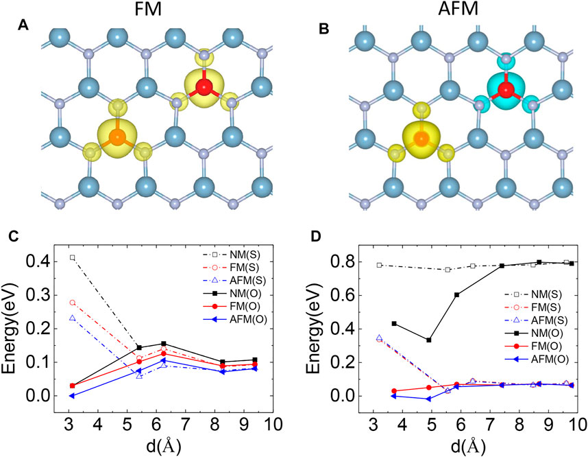
FIGURE 5. Representative spin density of monolayer AlN containing two SiAl defects in (A) FM and (B) AFM states, at a Si–Si separation of 5.4 Å. The isosurface of spin density is = 0.005 eV/Å3. The yellow and blue colors represent the positive and negative spin density, respectively. The energy of (C) monolayer AlN and (D) bilayer AlN with two SiAl defects on the same (S) and opposite (O) side of AlN sheet as a function of Si–Si separation. The magnetic coupling between Si can be in NM, FM, and AFM states. The energy of two SiAl defects with AFM coupling and the nearest distance was set to zero.
Si dopants should also exhibit magnetic moments in a few-layer AlN. We calculated the doping of Si in bilayer AlN with a stable AA’ stacking pattern [50]. We found that Si atoms also tend to substitute Al atoms in N-rich conditions and exhibit a magnetic moment of 1 μB per Si atom (Table 3). Two SiAl defects on opposite sides of the bilayer AlN have lower energy (Figure 5D). Si atoms also tend to get close to each other in bilayer AlN, similar to Si dopants in monolayer AlN (Figure 5D).
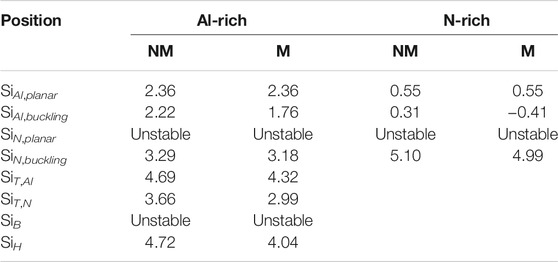
TABLE 3. Formation energies Ef (eV) of single Si atom in bilayer AlN in the magnetic (M) and non-magnetic (NM) states under Al- or N-rich growth conditions.
We noticed that the intrinsic defects of monolayer AlN, such as Al-vacancy and N-vacancy, can induce a non-zero magnetic monument [51]. We further found that the Al vacancy seems to have an AFM coupling with the Si dopants, thereby influencing the magnetic moment and magnetic coupling between the Si dopants. We will consider the effect of intrinsic defects on the magnetic properties of Si-doped AlN in later work.
By fully substituting the Al of monolayer AlN by Si, we obtained monolayer SiN which adopts a hexagonal lattice with a lattice constant of 2.904 Å and a buckling height of 0.578 Å. We compared different spin configurations of monolayer SiN (Figure 8A) and identified the FM state as its ground state. Thus, in Si-doped monolayer AlN, there should be a phase transition from an AFM to an FM state as the Si content increases.
We adopted the Dalpian’s band structure model to explain such phase transition [52]. There are four valence electrons per Si atom. As shown in Figure 3D, up-spin Si-2p states have higher energy than down-spin Si-2p states. An unpaired electron of Si produces a magnetic moment of 1 μB in the monolayer AlN. We used the ɛ↑, ɛ↓, △↑↑, and △↑↓ to represent the energy of spin-up and spin-down Si-2p states, hopping matrix elements among the Si-2p states with the same spins and different spins, respectively. When the magnetic coupling between Si dopants is FM, as shown in Figure 6A. From a molecular mode, the hybridization between the down-spin Si-2p states of the neighboring Si dopant produces molecular levels:
As the down-spin Si-2p states are fully filled, there is no energy gain from such hybridization. On the other hand, hybridization between the partially filled up-spin Si-2p states leads to an energy gain of −2|Δ↑↑|.
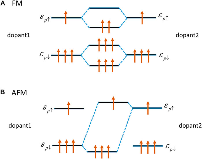
FIGURE 6. (A) FM interaction between the Si-2p states of same spin direction at the neighboring Si dopant. (B) The AFM interaction between the down-spin Si-2p states state and the up-spin Si-2p states of the neighboring Si dopant.
When the coupling between Si dopants is AFM, as shown in Figure 6B. The hybridization between the down-spin Si-2p states and the up-spin Si-2p states of the neighboring Si dopant produces molecular levels:
Similarly, the hybridization between the up-spin Si-2p states and the down-spin Si-2p states of the neighboring Si dopant will produce the same molecular levels. Moreover
Thus, the energy difference between the FM and AFM states is given as
At low Si concentration, the localized unpair p orbital of Si dopants leads to a small |△↑↑|. Adding the small exchange splitting (ɛ↑ − ɛ↓) (Figure 3D), ΔEFM−AFM is positive. Si-doped monolayer AlN exhibits the AFM state at low concentration. However, the lattice constant and the Si–Si distance of Si-doped AlN decrease as Si content increases. The unpaired p orbital of Si dopants becomes more delocalized and exchange splitting becomes large (Figure 7D), which results in the ground state of heavy Si-doped monolayer AlN changing to FM.
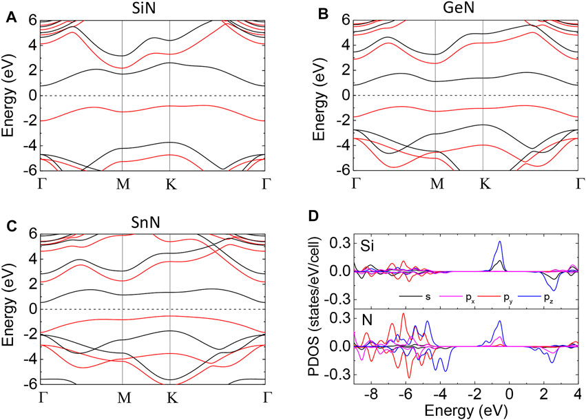
FIGURE 7. Band structure of monolayer (A) SiN, (B) GeN, and (C) SnN. The red and black lines represent the spin-up and spin-down bands, respectively. (D) The projected density of state of monolayer SiN.
The HSE band structure of FM monolayer AlN is shown in Figure 7A, indicating that it is a 2D FM semiconductor with an indirect band gap of 1.556 eV, consistent with previous work [53]. We considered four possible magnetic configurations, including FM, AFM1, AFM2, and AFM3 configurations (Figures 8A–D). We expanded their energy by the Heisenberg Hamiltonian:
where S is the spin per Si atom which was normalized to 1. J1, J2, and J3 are the nearest-neighboring, next-nearest-neighboring and thirdly-nearest-neighboring exchange interaction constants, respectively. We calculated these interaction constants through the relations between energy and spin configuration, the results are given in Table 4. Through the Monte Carlo simulation, the Curie temperature Tc of monolayer SiN was estimated to be about 105 K (Figure 8E).
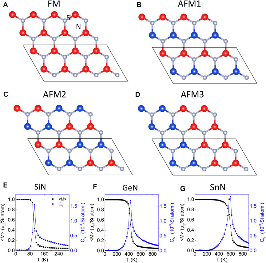
FIGURE 8. Monolayer XN (X = Si, Ge and Sn) in (A) FM, (B) AFM1, (C) AFM2, and (D) AFM3 states. Read and blue balls represent the Si atoms with up and down spin. (E–G) The averaged magnetization
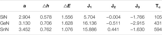
TABLE 4. Lattice constant a(Å), buckling height △h (Å), Band gap △E (eV), the nearest-neighboring, next-nearest-neighboring, thirdly-nearest-neighboring exchange interaction J1, J2 and J3 (meV), and Curie temperature Tc (K) of monolayer SiN, GeN, and SnN.
We expanded current calculations to Ge- and Sn-doped monolayer AlN. First, we found that single Ge and Sn dopants also prefer a magnetic buckling SiAl structure in monolayer AlN in the dilute doping scenario. The corresponding buckling height is 0.73 Å and 1.28 Å, respectively. Different from Si dopants, the Ge and Sn dopants in the planar SiAl structure are a saddle point, rather than a metastable state through the NEB calculations (Figures 4E,F). The diffusion barriers vertical to the AlN sheet are 0.6 and 1.0 eV for Ge and Sn dopants, respectively. Second, monolayers GeN and SnN are also 2D ferromagnetic semiconductors, with a band gap of 1.628 and 1.076 eV, respectively (Figures 7B,C). Their exchange constants are given in Table 4. Their Tc is estimated as 431 and 594 K through MC simulation, respectively (Figures 8F,G).
In summary, using first-principles calculations, we predicted that Si atoms are likely to substitute Al atoms in both bulk AlN and 2D AlN under N-rich growth conditions. Si atoms exhibit non-magnetic dopants and distribute homogeneously in bulk AlN. The diffusion of Si occurs more easily in the vertical direction [0001] of bulk AlN. In monolayer and bilayer AlN, substituted Si dopants prefer to form a buckling structure, with a magnetic moment of 1 μB per Si atom. The diffusion barrier of Si atoms is large along the AlN sheet, which can prevent the formation of Si clusters. The magnetic coupling among Si dopants in 2D AlN changes from AFM to FM coupling when the Si content increases due to the enhanced exchange splitting and delocalized impurity states of Si dopants. In the full substitution, monolayer SiN along with GeN and SnN are 2D FM semiconductors with a large band gap and high Curie temperature.
The original contributions presented in the study are included in the article/supplementary material; further inquiries can be directed to the corresponding author.
WW performed the calculations and wrote the manuscript with input from all authors. WW and NK analyzed the data. YG carried out the implementation. YL supervised the project.
This work was supported by the National Natural Science Foundation of China (Nos. 11904312 and 11904313), the Scientific Research Foundation of the Higher Education of Hebei Province, China (No. BJ2020015), the Natural Science Foundation of Hebei Province (Nos. A2019203507 and A2020203027), and the Doctor Foundation Project of Yanshan University (No. BL19008).
The authors declare that the research was conducted in the absence of any commercial or financial relationships that could be construed as a potential conflict of interest.
All claims expressed in this article are solely those of the authors and do not necessarily represent those of their affiliated organizations, or those of the publisher, the editors, and the reviewers. Any product that may be evaluated in this article, or claim that may be made by its manufacturer, is not guaranteed or endorsed by the publisher.
The numerical calculations in this paper have been done on the supercomputing system in the High Performance Computing Center of Yanshan University.
1. Dietl T, Bonanni A, Ohno H. Families of Magnetic Semiconductors - an Overview. J Semicond (2019) 40:080301. doi:10.1088/1674-4926/40/8/080301
2. Žutić I, Fabian J, Das Sarma S. Spintronics: Fundamentals and Applications. Rev Mod Phys (2004) 76:323–410. doi:10.1103/RevModPhys.76.323
3. Jungwirth T, Sinova J, Mašek J, Kučera J, MacDonald AH. Theory of Ferromagnetic (III,Mn)V Semiconductors. Rev Mod Phys (2006) 78:809–64. doi:10.1103/RevModPhys.78.809
4. Dietl T, Ohno H. Ferromagnetism in III-V and II-VI Semiconductor Structures. Physica E: Low-dimensional Syst Nanostructures (2001) 9:185–93. doi:10.1016/S1386-9477(00)00193-4
5. Singh R. Unexpected Magnetism in Nanomaterials. J Magnetism Magn Mater (2013) 346:58–73. doi:10.1016/j.jmmm.2013.07.005
6. Lungu II, Grumezescu AM, Fleaca C. Unexpected Ferromagnetism-A Review. Appl Sci (2021) 11:6707. doi:10.3390/app11156707
8. O'Leary SK, Foutz BE, Shur MS, Eastman LF. Steady-state and Transient Electron Transport within the III-V Nitride Semiconductors, GaN, AlN, and InN: A Review. J Mater Sci Mater Electron (2006) 17:87–126. doi:10.1007/s10854-006-5624-2
9. Tsipas P, Kassavetis S, Tsoutsou D, Xenogiannopoulou E, Golias E, Giamini SA, et al. Evidence for Graphite-like Hexagonal AlN Nanosheets Epitaxially Grown on Single crystal Ag(111). Appl Phys Lett (2013) 103:251605. doi:10.1063/1.4851239
10. Amorim RG, Zhong X, Mukhopadhyay S, Pandey R, Rocha AR, Karna SP. Strain- and Electric Field-Induced Band gap Modulation in Nitride Nanomembranes. J Phys Condens Matter (2013) 25:195801. doi:10.1088/0953-8984/25/19/195801
11. Ben J, Liu X, Wang C, Zhang Y, Shi Z, Jia Y, et al. 2D III‐Nitride Materials: Properties, Growth, and Applications. Adv Mater (2021) 33:2006761. doi:10.1002/adma.202006761
12. Khludkov SS, Prudaev IA, Root LO, Tolbanov OP, Ivonin IV. Aluminum Nitride Doped with Transition Metal Group Atoms as a Material for Spintronics. Russ Phys J (2021) 63:2013–24. doi:10.1007/s11182-021-02264-y
13. Sato K, H. Dederichs P, Katayama-Yoshida H. First-principles Study on the Ferromagnetism and Curie Temperature of Mn-Doped AlX and InX (X=N, P, as, and Sb). J Phys Soc Jpn (2007) 76:024717. doi:10.1143/jpsj.76.024717
14. Liu HX, Wu SY, Singh RK, Gu L, Smith DJ, Newman N, et al. Observation of Ferromagnetism above 900K in Cr-GaN and Cr-AlN. Appl Phys Lett (2004) 85:4076–8. doi:10.1063/1.1812581
15. Yao G, Fan G, Xing H, Zheng S, Ma J, Zhang Y, et al. Electronic Structure and Magnetism of V-Doped AlN. J Magnetism Magn Mater (2013) 331:117–21. doi:10.1016/j.jmmm.2012.11.031
16. Li H, Cai GM, Wang WJ. Room Temperature Luminescence and Ferromagnetism of AlN:Fe. AIP Adv (2016) 6:065025. doi:10.1063/1.4955100
17. Yang SL, Gao RS, Niu PL, Yu RH. Room-temperature Ferromagnetic Behavior of Cobalt-Doped AlN Nanorod Arrays. Appl Phys A (2009) 96:769–74. doi:10.1007/s00339-009-5269-0
18. Xiong J, Guo P, Cai Y, Stradel B, Brumek J, He Y, et al. Structural, Magnetic and Nanomechanical Properties in Ni-Doped AlN Films. J Alloys Compd (2014) 606:55–60. doi:10.1016/j.jallcom.2014.03.178
19. Li H, Chen XL, Song B, Bao HQ, Wang WJ. Copper-doped AlN Polycrystalline Powders: A Class of Room-Temperature Ferromagnetic Materials. Solid State Commun (2011) 151:499–502. doi:10.1016/j.ssc.2010.12.016
20. Wu QY, Huang ZG, Wu R, Chen LJ. Cu-doped AlN: a Dilute Magnetic Semiconductor Free of Magnetic Cations from First-Principles Study. J Phys Condens Matter (2007) 19:056209. doi:10.1088/0953-8984/19/5/056209
21. Li H, Wang W, Cai G. Controlled Synthesis of Al1−xZnx N with Blue Luminescence and Ferromagnetism Properties at Room temperatureZnN with Blue Luminescence and Ferromagnetism Properties at Room Temperature. J Magnetism Magn Mater (2018) 460:391–6. doi:10.1016/j.jmmm.2018.04.040
22. Fan SW, Yao KL, Huang ZG, Zhang J, Gao GY, Du GH. Ti-doped AlN Potential N-type Ferromagnetic Semiconductor: Density Functional Calculations. Chem Phys Lett (2009) 482:62–5. doi:10.1016/j.cplett.2009.09.062
23. Majid A, Azmat M, Rana UA, Khan SU-D, Alzahrani E. A Computational Study of Magnetic Exchange Interactions of 3d and 4f Electrons in Ti-Ce Co-doped AlN. Mater Chem Phys (2016) 179:316–21. doi:10.1016/j.matchemphys.2016.05.057
24. González-García A, López-Pérez W, González-Hernández R. Theoretical Study of Magnetic Ordering and Electronic Properties of AgxAl1−xN compoundsAlN Compounds. Solid State Commun (2011) 151:1794–7. doi:10.1016/j.ssc.2011.08.024
25. Han R, Yuan W, Yang H, Du X, Yan Y, Jin H. Possible Ferromagnetism in Li, Na and K-Doped AlN: A First-Principle Study. J Magnetism Magn Mater (2013) 326:45–9. doi:10.1016/j.jmmm.2012.08.026
26. Wu RQ, Peng GW, Liu L, Feng YP, Huang ZG, Wu QY. Ferromagnetism in Mg-Doped AlN from Ab Initio Study. Appl Phys Lett (2006) 89:142501. doi:10.1063/1.2358818
27. Zhang Y, Liu W, Liang P, Niu H. Half-metallic Ferromagnetism in Ca-Doped AlN from First-Principles Study. Solid State Commun (2008) 147:254–7. doi:10.1016/j.ssc.2008.06.008
28. Pan D, Jian JK, Sun YF, Wu R. Structure and Magnetic Characteristics of Si-Doped AlN Films. J Alloys Compd (2012) 519:41–6. doi:10.1016/j.jallcom.2011.12.015
29. Wang S, An Y, Xie C, Zhang H, Zeng Q. First-principles Prediction of Ferromagnetism in Transition-Metal Doped Monolayer AlN. Superlattices and Microstructures (2018) 122:171–80. doi:10.1016/j.spmi.2018.08.009
30. Bai Y, Deng K, Kan E. Electronic and Magnetic Properties of an AlN Monolayer Doped with First-Row Elements: a First-Principles Study. RSC Adv (2015) 5:18352–8. doi:10.1039/C4RA13522A
31. Han R, Chen X, Yan Y. Magnetic Properties of AlN Monolayer Doped with Group 1A or 2A Nonmagnetic Element: First-Principles Study. Chin Phys. B (2017) 26:097503. doi:10.1088/1674-1056/26/9/097503
32. Shi Z, Qi Z, Zang H, Jiang K, Chen Y, Jia Y, et al. Point Defects in Monolayer H-AlN as Candidates for Single-Photon Emission. ACS Appl Mater Inter (2021) 13:37380–7. doi:10.1021/acsami.1c09175
33. Kadioglu Y, Ersan F, Kecik D, Aktürk OÜ, Aktürk E, Ciraci S. Chemical and Substitutional Doping, and Anti-site and Vacancy Formation in Monolayer AlN and GaN. Phys Chem Chem Phys (2018) 20:16077–91. doi:10.1039/C8CP02188K
34. Gupta SK, He H, Banyai D, Si M, Pandey R, Karna SP. Effect of Si Doping on the Electronic Properties of BN Monolayer. Nanoscale (2014) 6:5526–31. doi:10.1039/C4NR00159A
35. Kresse G, Hafner J. Ab Initiomolecular Dynamics for Liquid Metals. Phys Rev B (1993) 47:558–61. doi:10.1103/PhysRevB.47.558
36. Kresse G, Furthmüller J. Efficient Iterative Schemes Forab Initiototal-Energy Calculations Using a Plane-Wave Basis Set. Phys Rev B (1996) 54:11169–86. doi:10.1103/PhysRevB.54.11169
37. Kresse G, Joubert D. From Ultrasoft Pseudopotentials to the Projector Augmented-Wave Method. Phys Rev B (1999) 59:1758–75. doi:10.1103/PhysRevB.59.1758
38. Perdew JP, Burke K, Ernzerhof M. Generalized Gradient Approximation Made Simple. Phys Rev Lett (1996) 77:3865–8. doi:10.1103/PhysRevLett.77.3865
39. Monkhorst HJ, Pack JD. Special Points for Brillouin-Zone Integrations. Phys Rev B (1976) 13:5188–92. doi:10.1103/PhysRevB.13.5188
40. Heyd J, Scuseria GE, Ernzerhof M. Hybrid Functionals Based on a Screened Coulomb Potential. J Chem Phys (2003) 118:8207–15. doi:10.1063/1.1564060
41. Liu L, Ren X, Xie J, Cheng B, Liu W, An T, et al. Magnetic Switches via Electric Field in BN Nanoribbons. Appl Surf Sci (2019) 480:300–7. doi:10.1016/j.apsusc.2019.02.203
43. Hermann M, Furtmayr F, Bergmaier A, Dollinger G, Stutzmann M, Eickhoff M. Highly Si-Doped AlN Grown by Plasma-Assisted Molecular-Beam Epitaxy. Appl Phys Lett (2005) 86:192108. doi:10.1063/1.1923180
44. Lyons JL, Wickramaratne D, Van de Walle CG. A First-Principles Understanding of point Defects and Impurities in gan. J Appl Phys (2021) 129:111101. doi:10.1063/5.0041506
45. Zhang Y, Liu W, Niu H. Native Defect Properties and P-type Doping Efficiency in Group-IIA dopedwurtziteAlN-type Doping Efficiency in Group-IIA Doped Wurtzite AlN. Phys Rev B (2008) 77:035201. doi:10.1103/PhysRevB.77.035201
46. Mills G, Jónsson H, Schenter GK. Reversible Work Transition State Theory: Application to Dissociative Adsorption of Hydrogen. Surf Sci (1995) 324:305–37. doi:10.1016/0039-6028(94)00731-4
47. Xiao G, Wang L-L, Rong Q-Y, Hu A-M, Xiao W-Z. Magnetic Properties in AlN Nanosheet Doped with Alkali Metals: A First-Principles Study. Phys Status Solidi B (2016) 253:1816–23. doi:10.1002/pssb.201600119
48. Kanoun MB, Goumri-Said S, Schwingenschlögl U. Ferromagnetism in Cr-Doped Passivated AlN Nanowires. J Mater Chem A (2014) 2:9287–90. doi:10.1039/C4TA00593G
49. Mansurov V, Malin T, Galitsyn Y, Zhuravlev K. Graphene-like AlN Layer Formation on (111)Si Surface by Ammonia Molecular Beam Epitaxy. J Cryst Growth (2015) 428:93–7. doi:10.1016/j.jcrysgro.2015.07.030
50. Bacaksiz C, Sahin H, Ozaydin HD, Horzum S, Senger RT, Peeters FM. Hexagonal AlN: Dimensional-Crossover-Driven Band-gap Transition. Phys Rev B (2015) 91:085430. doi:10.1103/PhysRevB.91.085430
51. Nayeri M, Akherati P. The Influence of Intrinsic Atomic Defects on the Electronic and Optical Properties of the Single Layer AlN. Phys Scr (2020) 95:075106. doi:10.1088/1402-4896/ab93a7
52. Dalpian GM, Wei S-H, Gong XG, da Silva AJR, Fazzio A. Phenomenological Band Structure Model of Magnetic Coupling in Semiconductors. Solid State Commun (2006) 138:353–8. doi:10.1016/j.ssc.2006.03.002
Keywords: aluminum nitride, silicon doping, magnetic semiconductor, diffusion, Curie temperature
Citation: Wan W, Kang N, Ge Y and Liu Y (2022) The Theoretical Study of Unexpected Magnetism in 2D Si-Doped AlN. Front. Phys. 10:843352. doi: 10.3389/fphy.2022.843352
Received: 25 December 2021; Accepted: 14 February 2022;
Published: 11 March 2022.
Edited by:
Xiao-Ping Wei, Lanzhou Jiaotong University, ChinaReviewed by:
Altaf Ur Rahman, Riphah International University, PakistanCopyright © 2022 Wan, Kang, Ge and Liu. This is an open-access article distributed under the terms of the Creative Commons Attribution License (CC BY). The use, distribution or reproduction in other forums is permitted, provided the original author(s) and the copyright owner(s) are credited and that the original publication in this journal is cited, in accordance with accepted academic practice. No use, distribution or reproduction is permitted which does not comply with these terms.
*Correspondence: Yong Liu, eW9uZ2xpdUB5c3UuZWR1LmNu
Disclaimer: All claims expressed in this article are solely those of the authors and do not necessarily represent those of their affiliated organizations, or those of the publisher, the editors and the reviewers. Any product that may be evaluated in this article or claim that may be made by its manufacturer is not guaranteed or endorsed by the publisher.
Research integrity at Frontiers
Learn more about the work of our research integrity team to safeguard the quality of each article we publish.