- Zhongshan Institute, University of Electronic Science and Technology of China, Zhongshan, Guangdong, China
A 10 bit 1 MS/s SAR ADC with one LSB common-mode shift energy-efficient switching scheme for image sensor is presented. Based on the two sub-capacitor arrays architecture and the common-mode technique, the proposed switching scheme achieves 98.45% less switching energy over the conventional architecture with common-mode shift in one LSB. The comparator uses a low power dynamic comparator. The sampling switch adopts a bootstrap circuit with low sampling error. SAR logic is composed of Bit-Slice circuit with low power consumption and few transistors. Simulated in 180 nm CMOS process and 1 MS/s sampling rate, the ADC achieves the 60.06 dB SNDR, the 75.43 dB SFDR and the 10.45 μW power consumption.
1 Introduction
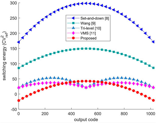
In recent years, successive approximation register (SAR) analog-to-digital converter (ADC) has been widely used in image sensors because of its low power consumption [1–4]. Figure 1 shows the basic processing units in a image sensor application, ADC is an intermediate unit that converts analog signals into digital signals. Among the components of SAR ADC, the energy consumed by capacitor array DAC accounts for a large part of the total energy consumed [5–7]. In order to improve the power efficiency of capacitor DAC, some energy-efficient switching schemes [8–11] have been proposed. Compared to a conventional switching scheme [12], set and down [8], Wang [9], Tri-level [10], and VMS [11] reduce the switching energy by 81.26%, 90.61%, 96.89%, and 97.66%, respectively. However, common-mode shift of these schemes is large.
In this paper, a new one LSB common-mode shift energy-efficient switching scheme is proposed to reduce common-mode shift. Based on the two sub-capacitor arrays architecture and the common-mode technique, the average switching energy of the proposed one LSB common-mode shift switching scheme for 10-bit SAR ADC is 21.08
This paper is organized as follows. Section 2 explains the proposed SAR ADC architecture, which includes various low-power design technologies, such as one LSB common-mode shift energy-efficient switching scheme, dynamic comparator, bootstrap sampling switch, SAR logic based on dynamic circuit, etc.; The simulated results and the comparison with the state of the art are shown in Section 3. Finally, Section 4 concludes this article.
2 Proposed SAR ADC
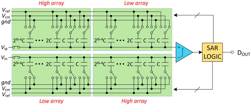
The N-bit SAR ADC of the proposed architecture is shown in Figure 2. The SAR ADC consists of DAC, comparator, sampling switch and SAR logic. The DAC consists of positive capacitor array and negative capacitor array, and each array is composed of the same two sub-capacitor arrays (high array and low array).
2.1 Proposed one LSB common-mode shift switching scheme
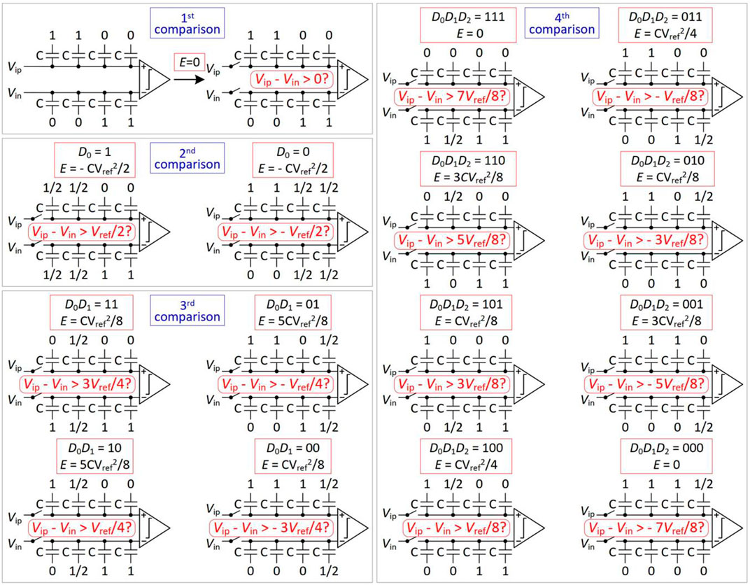
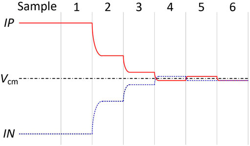
To explain the operation of the proposed one LSB common-mode shift switching scheme, a 4-bit proposed SAR ADC is used. As shown in Figure 3, the operation includes four phases: 1st comparison, 2nd comparison, 3rd to (N-1)th comparison and Nth comparison.
1st comparison: The reference voltages of the high arrays are connected to
2nd comparison: If D1 = 1, the reference voltages of the high array in positive capacitor array and the low array in negative capacitor array become
3rd to (N-1)th comparison: From the third comparison to the (N-1)th comparison, according to the results of the previous comparison, the reference voltage of the corresponding capacitor in the high-voltage capacitor array changes from
Nth comparison: If DN-1 = 1, the reference voltage of the last capacitor connected to
The average switching energy of proposed one LSB common-mode shift switching scheme for N-bit SAR ADC is:
2.2 Comparator
Dynamic comparators are widely used in ADCs because of their low power consumption. In the application of the dynamic comparator, the NMOS is generally used as the input port [18–21]. As shown in Figure 4, in order to improve the accuracy of comparison, this paper uses PMOS as the input port for low VDD. The comparator work is divided into two phases. In the first phase, when CLK is high, MC1 is OFF, the paths connecting A and B to VDD are OFF, MC6, MC7, MC10, and MC11 are ON, A and B are connected to ground, and the output ports OUTP and OUTN are high. In the second phase, CLK is low, MC6, MC7, MC10, and MC11 are OFF, the paths from A and B to ground are disconnected, MC1 is ON, VDD charges A through MC1, MC2, and MC4, and through MC1, MC3, and MC5 charges B. The charging speed is related to the voltage of IP and IN. If IP > IN, the voltage of A is greater than the voltage of B. Since MC4, MC5, MC8, and MC9 constitute a positive feedback latch circuit, eventually the voltage of A will become low, the voltage of B will become high, OUTP will become high, and OUTN will become low level. If IP < IN, then finally the voltage of A will become high, the voltage of B will become low, OUTP will become low, and OUTN will become high. During the operation of the comparator, there is no DC path from VDD to ground, so only dynamic power is consumed.
2.3 Sampling switch
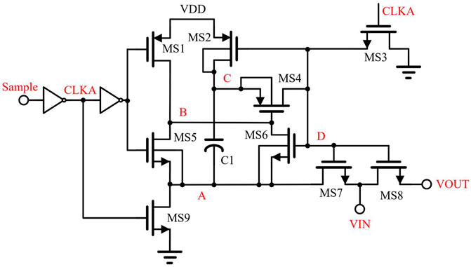
In order to reduce the sampling error, the sampling switch generally adopts a bootstrap circuit [13, 14]. As shown in Figure 5, the bootstrap process is divided into two phases. In the first phase, when Sample is low, CLKA is high, MS1, MS2, MS3, and MS9 are ON, and MS4, MS5, MS6, MS7, and MS8 are OFF. At this time, A and D are low, B and C are high. In the second phase, when sample is high, CLKA is low, MS1, MS2, MS3, and MS9 are OFF, MS4, MS5, MS6, MS7, and MS8 are ON, so the voltages of A and B are the input signals VIN, The voltages of C and D are bootstrapped as VDD + VIN. So the sampling switch MS8 realizes the bootstrap sampling.
2.4 SAR logic
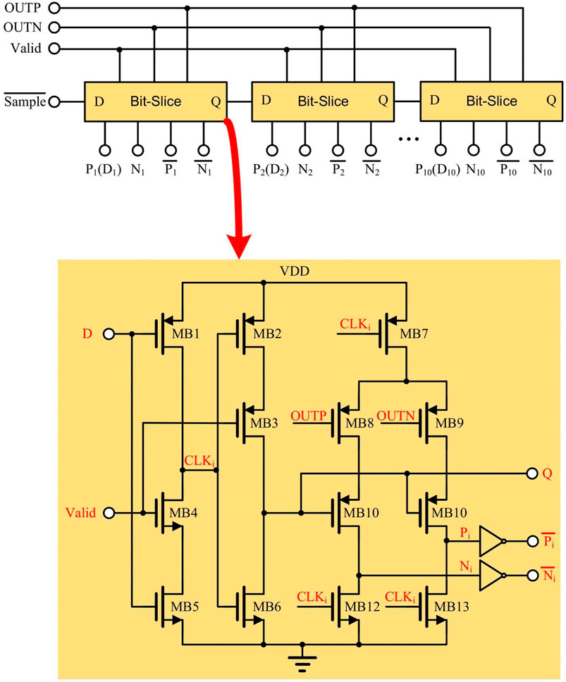
The conventional SAR logic uses D flip-flop [8, 22, 23], which requires a large number of transistors and consumes a lot of power. In order to reduce the power consumption of the SAR logic, some papers use Bit-Slice circuit [15–17]. The Bit-slice circuit has fewer transistors and lower power consumption. As shown in Figure 6, during the sampling phase, Sample and Valid are high, Pi and Ni are low,
3 Simulation results and discussion
Several switching schemes for 10-bit SAR ADC are simulated in MATLAB. The average switching energy of the proposed one LSB common-mode shift switching scheme for 10 bit SAR ADC is 21.08

TABLE 1. Comparison of energy saving and Common-mode shift for different switching schemes of a 10-bit SAR ADC.
The transient simulation of the comparator is shown in Figure 10A. The differential input signals IP and IN of the comparator are 752.5 mV and 747.5 mV respectively. It can be seen from the figure that when CLK drops to low, A and B first increase the voltage together, and then gradually separate, one becomes higher and the other becomes lower. Finally, OUTP and OUTN become one high and one low. The comparator completes the output of comparison results. As shown in Figure 10B, the offset voltage of the dynamic comparator is 950.452 μV after 500 Monte Carlo simulations. The offset voltage does not exceed 1.46 (1,500/1,024) mV.
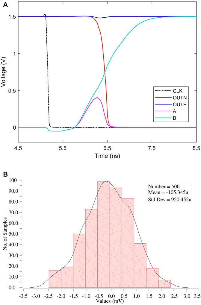
FIGURE 10. Simulation of dynamic comparator. (A) Transient simulation. (B) Monte Carlo simulation of the offset voltage.
The transient simulation diagram of bootstrap sampling switch is shown in Figure 11A. It can be seen from the figure that when the sampling signal sample is high, the control signal D of the sampling switch is bootstrapped up and changes with the input signal VIN. Therefore, VGS of transistor MS8 remains unchanged during sampling, thus reducing the sampling error. Figure 11B shows the spectrum analysis results of the bootstrap sampling switch. The SFDR and SNDR are 94.13 dB and 93.81 dB respectively, and the ENOB of the sampled signal is 15.29 bit, which can meet the requirements of 10 bit SAR ADC.
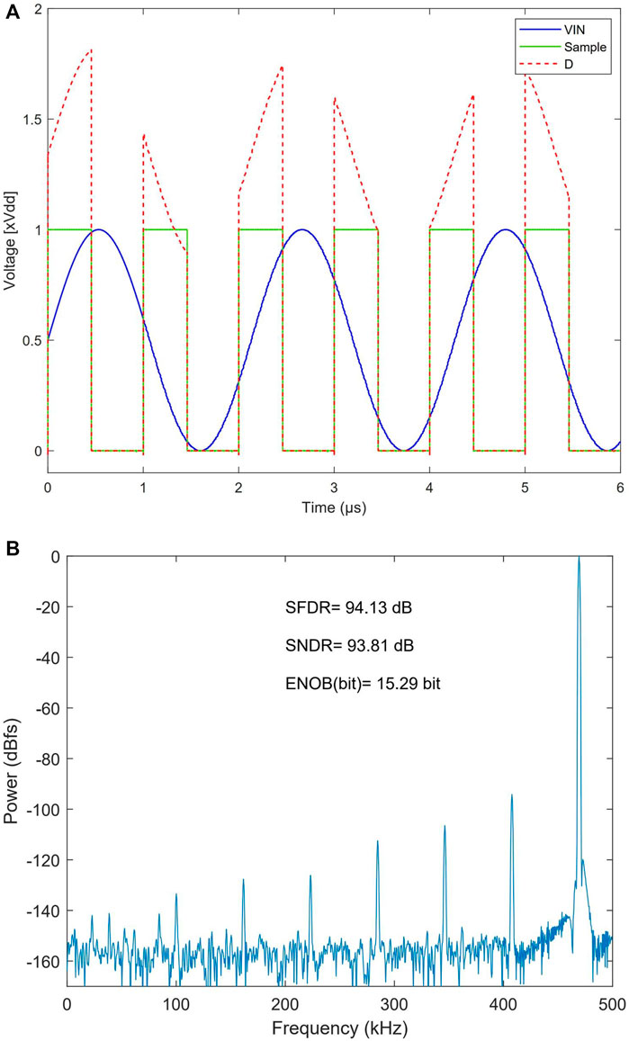
FIGURE 11. Simulation of bootstrapped sampling switch. (A) Transient simulation. (B) FFT of Bootstrapped sampling switch.
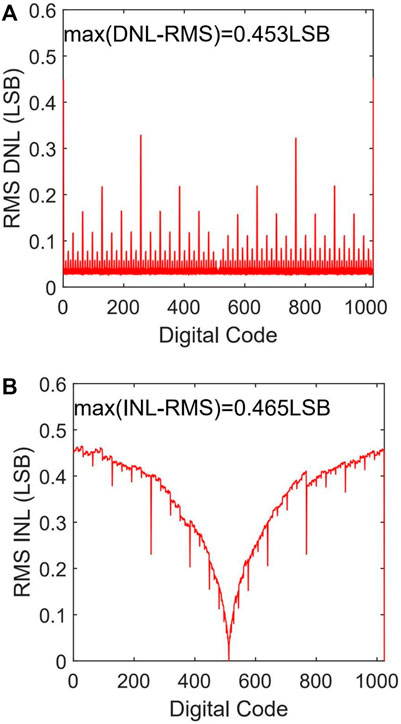
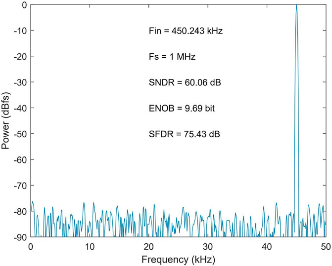
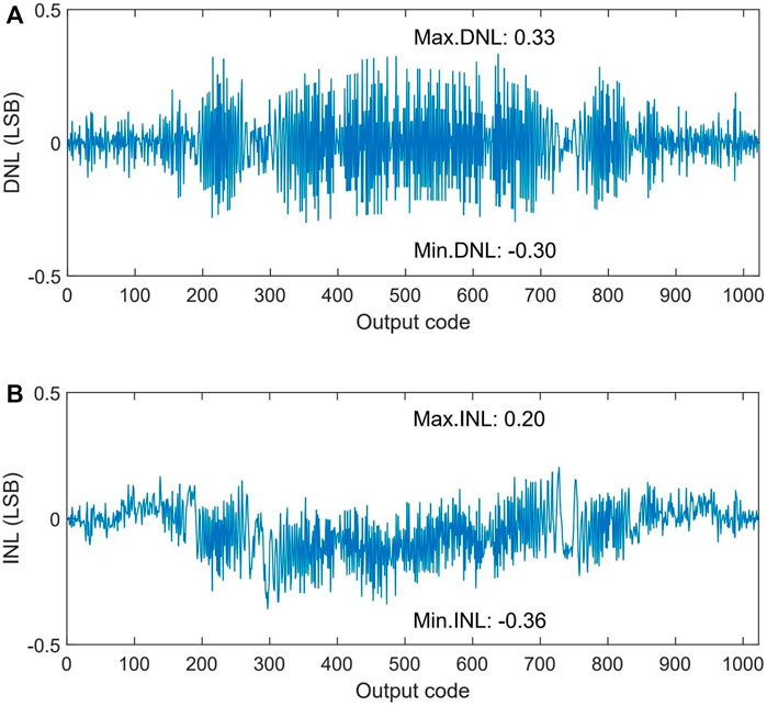
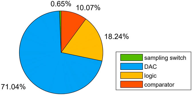
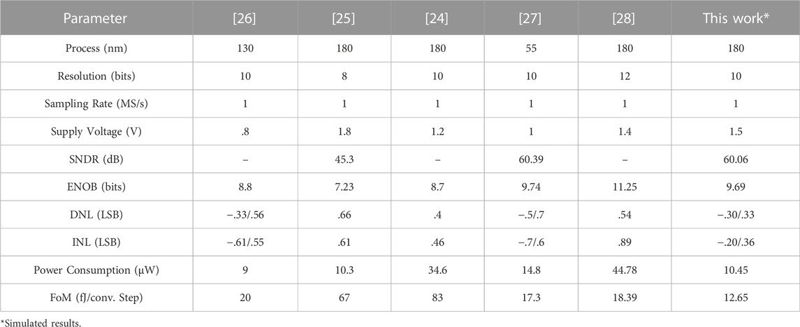
The proposed SAR ADC was designed and simulated using 180 nm CMOS technology. The simulation settings are as follows: the power supply is 1.5V, the full swing input signal frequency is 450.243 kHz, and the sampling rate is 1 MS/s. Figure 12 shows the FFT spectrum of the proposed SAR ADC. The ADC achieves 75.43 dB spurious-free dynamic range (SFDR) and 60.06 dB signal-to-noise and distortion ratio (SNDR), respectively. Figures 13A, B show the variation of SFDR and SNDR with input signal frequency and sampling frequency. The simulated DNL and INL of the proposed SAR ADC are shown in Figure 14A, B. The peak DNL and INL are −.30–+.33 LSB and −.36–+.20 LSB, which are both less than .5 LSB. The proposed SAR ADC has a total power consumption of 10.45 μW. Figure 15 shows the percentage of each circuit module in the total power consumption of the SAR ADC. Performance comparison of various ADC [24–28] is shown in Table 2. The proposed SAR ADC is suitable for image sensors. The Figure-of-Merit (FoM) was calculated from the following equation:
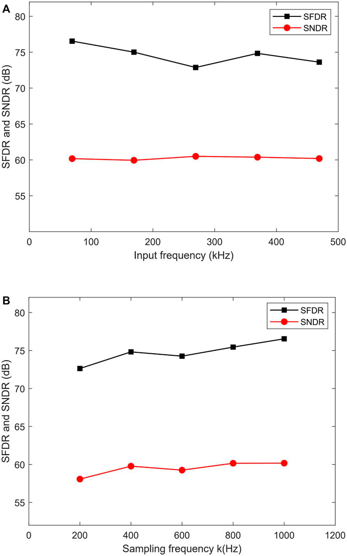
FIGURE 13. SNDR/SFDR with various input frequencies and various sampling frequencies. (A) Various input frequencies. (B) Various sampling frequencies.
4 Conclusion
This paper has presented a 10 bit 1 MS/s low-power SAR ADC for image sensors. The proposed SAR ADC consists of DAC, dynamic comparator, bootstrap sampling switch and SAR logic. The DAC consists of positive capacitor array and negative capacitor array, and each array is composed of the same two sub-capacitor arrays. Based on these sub-capacitor arrays, the DAC uses a one LSB common-mode shift energy-efficient switching scheme to reduce power consumption. Compared with conventional switching scheme, the proposed switching scheme achieves an energy savings of 98.45%. In addition, the simulation shows that the offset voltage of the comparator and the ENOB of the sampling switch meet the requirements of ADC. Bit-Slice circuit makes the power consumption of SAR logic lower and the number of transistors less. Simulated in 180 nm CMOS process and 1 MS/s sampling rate, the ADC achieves 75.43 dB SFDR, 60.06 dB SNDR and 10.45 μW power consumption. The FoM of the proposed SAR ADC is 12.65 fJ/conv.-step. The proposed low-power SAR ADC is suitable for image sensors.
Data availability statement
The original contributions presented in the study are included in the article/Supplementary Material, further inquiries can be directed to the corresponding author.
Author contributions
YH: Conceived the project, organized the paper content, wrote and edited the manuscript. LH: Designed and simulated the circuit. BT: Drawn the figure. ZY: Edited the manuscript.
Funding
This work was financially supported by the Key Field Project of Colleges and Universities in Guangdong Province (Grant no. 2022ZDZX1044), the Key Project of Social Welfare and Basic Research Project in Zhongshan City (Grant no. 2021B2020), the Construction Project of Professional Quality Engineering in 2020 (Grant no. YLZY202001), the Construction Project of Professional Quality Engineering in 2021 (Grant no. JD202101).
Conflict of interest
The authors declare that the research was conducted in the absence of any commercial or financial relationships that could be construed as a potential conflict of interest.
Publisher’s note
All claims expressed in this article are solely those of the authors and do not necessarily represent those of their affiliated organizations, or those of the publisher, the editors and the reviewers. Any product that may be evaluated in this article, or claim that may be made by its manufacturer, is not guaranteed or endorsed by the publisher.
References
1. Jin-Yi L, Kwuang-Han C, Chen-Che K, Shih-Chin L, Yan-Jiun C, Pei-Chen L, et al. An 8-bit column-shared sar adc for cmos image sensor applications. In: 2015 IEEE International Symposium on Circuits and Systems (ISCAS). Lisbon, Portugal: IEEE (2015). 301–4. doi:10.1109/ISCAS.2015.7168630
2. Xie S, Theuwissen A. A 10 bit 5 Ms/S column sar adc with digital error correction for cmos image sensors. IEEE Trans Circuits Syst Express Briefs (2020) 67(6):984–8. doi:10.1109/tcsii.2019.2928204
3. Zhang X, Fan W, Xi J, He L. 14-Bit fully differential sar adc with pga used in readout circuit of cmos image sensor. J Sens (2021) 2021:2021–17. doi:10.1155/2021/6651642
4. Choo KD, Xu L, Kim Y, Seol J, Wu X, Sylvester D, et al. Energy-efficient motion-triggered iot cmos image sensor with capacitor array-assisted charge-injection sar adc. IEEE J Solid-state Circuits (2019) 54(11):2921–31. doi:10.1109/JSSC.2019.2939664
5. Byung-Geun L. Power and bandwidth scalable 10-B 30-ms/S sar adc. IEEE Trans Very Large Scale Integr VLSI Syst (2015) 23(6):1103–10. doi:10.1109/TVLSI.2014.2331354
6. Lin JY, Hsieh CC. A 0.3 V 10-bit 1.17 F sar adc with merge and split switching in 90 Nm cmos. IEEE Trans Circuits Syst Regul Pap (2015) 62(1):70–9. doi:10.1109/TCSI.2014.2349571
7. Zhangming Z, Yuhua L. A 0.6-V 38-nw 9.4-enob 20-ks/S sar adc in 0.18-um cmos for medical implant devices. IEEE Trans Circuits Syst Regul Pap (2015) 62(9):2167–76. doi:10.1109/TCSI.2015.2451812
8. Liu CC, Chang SJ, Huang GY, Lin YZ. A 10-bit 50-ms/S sar adc with a monotonic capacitor switching procedure. IEEE J Solid-state Circuits (2010) 45(4):731. doi:10.1109/Jssc.2010.2042254
9. Wang H, Zhu Z. Energy-efficient and reference-free monotonic capacitor switching scheme with fewest switches for sar adc. IEICE Electron Expr (2015) 12(7):20141202. doi:10.1587/elex.12.20141202
10. Yuan C, Lam Y. Low-energy and area-efficient tri-level switching scheme for sar adc. Electron Lett (2012) 48(9):482–3. doi:10.1049/el.2011.4001
11. Zhangming Z, Yu X, Xiaoli S. Vcm-based monotonic capacitor switching scheme for sar adc. Electron Lett (2013) 49(5):327–9. doi:10.1049/el.2012.3332
13. Abo AM, Gray PR. A 1.5-V, 10-bit, 14.3-ms/S cmos pipeline analog-to-digital converter. IEEE J Solid-state Circuits (1999) 34(5):599–606. doi:10.1109/4.760369
14. Zhu Z, Xiao Y, Liang L, Liu L, Yang Y. A 3.03 Μw 10-bit 200 Ks/S sar adc in 0.18 Μm cmos. J Circuits Syst Comput (2013) 22(4):1350026. doi:10.1142/s0218126613500266
15. Harpe PJA, Zhou C, Yu B, van der Meijs NP, Xiaoyan W, Philips K, et al. A 26 Μw 8 bit 10 Ms/S asynchronous sar adc for low energy radios. IEEE J Solid-state Circuits (2011) 46(7):1585–95. doi:10.1109/jssc.2011.2143870
16. Zhu Z, Xiao Y, Wang W, Wang Q, Yang Y. A 0.6 V 100 Ks/S 8-10 B resolution configurable sar adc in 0.18 Μm cmos. Analog Integr Circ S (2013) 75(2):335–42. doi:10.1007/s10470-013-0062-6
17. Zhu Z, Xiao Y, Xu L, Ding H, Yang Y. An 8/10 Bit 200/100ms/S Configurable Asynchronous Sar Adc. Analog Integr Circ S (2013) 77 (2):249–255. doi:10.1007/s10470-013-0133-8
18. Schinkel D, Mensink E, Klumperink E, Ev T, Nauta B. A double-tail latch-type voltage sense amplifier with 18ps Setup+Hold time. In: 2007 IEEE International Solid-State Circuits Conference Digest of Technical Papers. San Francisco, CA, USA: IEEE (20072007). p. 11314–605. doi:10.1109/ISSCC.2007.373420
19. Babayan-Mashhadi S, Lotfi R. Analysis and design of a low-voltage low-power double-tail comparator. IEEE Trans Very Large Scale Integr VLSI Syst (2014) 22(2):343–52. doi:10.1109/TVLSI.2013.2241799
20. Savani V, Devashrayee NM. Analysis and design of low-voltage low-power high-speed double tail current dynamic latch comparator. Analog Integr Circ S (2017) 93(2):287–98. doi:10.1007/s10470-017-1040-1
21. Wicht B, Nirschl T, Schmitt-Landsiedel D. Yield and speed optimization of a latch-type voltage sense amplifier. IEEE J Solid-state Circuits (2004) 39(7):1148–58. doi:10.1109/JSSC.2004.829399
22. Liu CC, Huang YT, Huang GY, Chang SJ, Huang CM, Huang CH. A 6-bit 220-ms/S time-interleaving sar adc in 0.18-µm digital cmos process. In: 2009 International Symposium on VLSI Design, Automation and Test. Hsinchu: IEEE (2009). p. 215–8. doi:10.1109/VDAT.2009.5158133
23. Cao ZH, Yan SL, Li YC. A 32 Mw 1.25 Gs/S 6b 2b/step sar adc in 0.13 mu M cmos. IEEE J Solid-state Circuits (2009) 44(3):862. doi:10.1109/Jssc.2008.2012329
24. Saisundar S, Jia HC, Minkyu J. A 1.8v 1ms/S rail-to-rail 10-bit sar adc in 0.18mum cmos. In: 2012 IEEE International Symposium on Radio-Frequency Integration Technology (RFIT). Singapore: IEEE (2012). p. 83–5. doi:10.1109/rfit.2012.6401621
25. Wen-Cheng L, Jhin-Fang H, Wei-Jian L. 1ms/S low power successive approximations register adc for 67-fj/conversion-step. In: 2012 IEEE Asia Pacific Conference on Circuits and Systems. Kaohsiung, Taiwan: IEEE (2012). p. 260–3. doi:10.1109/APCCAS.2012.6419021
26. Yonghong T, Yong L. A 0.8-V, 1-ms/S, 10-bit sar adc for multi-channel neural recording. IEEE Trans Circuits Syst Regul Pap (2015) 62(2):366–75. doi:10.1109/TCSI.2014.2360762
27. Verma D, Shehzad K, Khan D, Kim SJ, Pu YG, Yoo S-S, et al. A design of low-power 10-bit 1-ms/S asynchronous sar adc for dsrc application. Electronics (2020) 9(7):1100. doi:10.3390/electronics9071100
Keywords: image sensor, SAR ADC, switching scheme, energy-efficient, common-mode shift
Citation: Hu Y, Hu L, Tang B and Yi Z (2022) A 10 bit 1 MS/s SAR ADC with one LSB common-mode shift energy-efficient switching scheme for image sensor. Front. Phys. 10:1102674. doi: 10.3389/fphy.2022.1102674
Received: 19 November 2022; Accepted: 15 December 2022;
Published: 23 December 2022.
Edited by:
Qiang Xu, Nanyang Technological University, SingaporeReviewed by:
Rui Yao, China University of Mining and Technology, ChinaFuyuan Hu, Suzhou University of Science and Technology, China
Copyright © 2022 Hu, Hu, Tang and Yi. This is an open-access article distributed under the terms of the Creative Commons Attribution License (CC BY). The use, distribution or reproduction in other forums is permitted, provided the original author(s) and the copyright owner(s) are credited and that the original publication in this journal is cited, in accordance with accepted academic practice. No use, distribution or reproduction is permitted which does not comply with these terms.
*Correspondence: Yunfeng Hu, aHV5ZkB6c2MuZWR1LmNu
 Yunfeng Hu
 Lexing Hu
 Bin Tang
 Zichuan Yi
