
95% of researchers rate our articles as excellent or good
Learn more about the work of our research integrity team to safeguard the quality of each article we publish.
Find out more
ORIGINAL RESEARCH article
Front. Phys. , 16 February 2023
Sec. Condensed Matter Physics
Volume 10 - 2022 | https://doi.org/10.3389/fphy.2022.1091325
In this work, we investigate the thermoelectrical properties of a silicene nanoribbon heterostructure composed of a central conductor fully doped with ad-atoms and connected to two pristine leads of the same material. Using a tight-binding Hamiltonian, we have calculated the system’s thermoelectric properties as a function of the geometrical confinement and external field. Our results exhibit an enhancement of the thermopower when a transverse electric field is applied to the conductor region for different temperatures. In addition, a violation of the Wiedemann–Franz law is observed around the ad-atom energy. Our results suggest the thermoelectric properties of doped silicene nanoribbons can be efficiently tuned with external perturbations.
In thermal devices, the capacity to transform heat into electricity and vice versa is characterized by the thermoelectric efficiency, which is usually described in terms of the dimensionless quantity ZT = S2GT/κ called the figure of merit [1]. In this definition, S is the thermopower or Seebeck coefficient, G is the electronic conductance, and κ is thermal conductance at a temperature T, respectively. It is well known that in a thermoelectric system, both electrons and phonons contribute to heat current. Then, the thermal conductance can be written as κ = κel+κph when the electron–phonon coupling is weak. To obtain an enhanced thermoelectric efficiency, it is necessary to simultaneously reduce both contributions to the thermal conductance without affecting electronic conduction. It cannot be obtained in bulk metallic materials due to the classical Wiedemann–Franz law, which establishes that the ratio σT/κel is a universal constant. Thus, a possible route to improve the thermoelectric materials could be a controlled reduction of the lattice thermal conductance κph by increasing phonon scattering [2]. In the last few years, several works have provided theoretical [3–6] and experimental evidence [7–11] that nanostructuring yields thermoelectric efficiency unachievable with bulk materials. In these nanometer systems, the thermal and electronic properties can be tuned independently to achieve improved efficiency above the classical limit. In the literature, ZT values greater than 2.4 have been reported in tailored nanostructured materials such as superlattices [7], nanowires [9], quantum dots [8], or in weak-coupling molecular junctions with electrode doping [12]. Therefore, in this context, nanostructures made of silicene sheets and silicene nanoribbons seem to be good candidates to exhibit high thermoelectric efficiencies [13,14]. Bulk silicene exhibits an in-plane thermal conductivity of 20 W/mK at room temperature, according to equilibrium molecular dynamics simulations [15]. This value is one order of magnitude lower than that of silicon. Silicene has a honeycomb lattice structure, but due to the large ionic radius of silicon atoms, buckling of the lattice is induced [16,17]. Buckling impacts the vibrational modes of silicene, reducing phonon heat conduction. Finally, the quantum effects allow thermoelectric devices to overcome the limitations to the classical Wiedemann–Franz law. Nanodevices with sharp resonances in electron transmission (such as Fano lineshapes) are good candidates for highly efficient heat-to-electricity converters because the ratio GT/κel increases well above the classical Wiedemann–Franz limit [18–24].
In this context, we have studied the thermoelectric properties of the doped silicene nanoribbon heterostructure as a function of the geometrical confinement and the presence of an external electric field. Considering a central conductor region fully doped with ad-atoms and connected to two pristine leads, we calculated the electronic conductance, the Seebeck coefficient, the electronic thermal conductance, the Lorenz number, and the electronic figure of merit of armchair silicene nanoribbons. We have found an enhancement of the thermopower of the device at different temperatures when a transverse electric field is applied to the conductor region. Consequently, we have obtained great values of ZTel as the external potential is increased for different temperatures. Finally, we have obtained a violation of the Wiedemann–Franz law for different external potential intensities and temperatures. Our results suggest that with an appropriate gate configuration, the thermoelectric properties of doped silicene nanoribbons can be efficiently tuned.
The system under the study consists of a fully doped rectangular silicene nanoribbon (SNR) of width W and length L connected to source and drain leads made of pristine SNRs, as shown schematically in Figure 1. To avoid topologically protected edge states that appear at the Fermi energy in zig-zag nanoribbons, we restrict ourselves to nanoribbons with armchair edges (A-SNR) hereafter. Electronic properties in these ribbons have been described by using a single-band tight-binding approximation [25]. For this purpose, the system is split into three spatial regions: left contact, scattering region (conductor), and right contact. The Hamiltonian of the doped A-SNR ribbon can be written in the single-band tight-binding scheme as follows:
where
where Γ is the coupling between the ad-atoms and the ribbon’s A(B) atoms. UE = l E is the electrostatic potential generated by the electric field E, considering l as the vertical separation between both sub-lattices in the ribbon; therefore, ɛU(D) = ɛ0 ± UE. We introduce the parameter α as a measure of ribbon buckling so that 0 ≤ α ≤ 1. It should be noticed that if the ribbon is planar (α = 0), the electrostatic potential affects only the energy of the ad-atoms. Therefore, a differentiation is generated between both sub-lattices of the ribbon. On the other hand, if α ≠ 0, the electrostatic potential affects both ribbons’ sub-lattices (staggered potential) and the ad-atoms. Therefore, this electrostatic potential’s effects on the buckled ribbon’s electronic properties are stronger than those in the planar case.
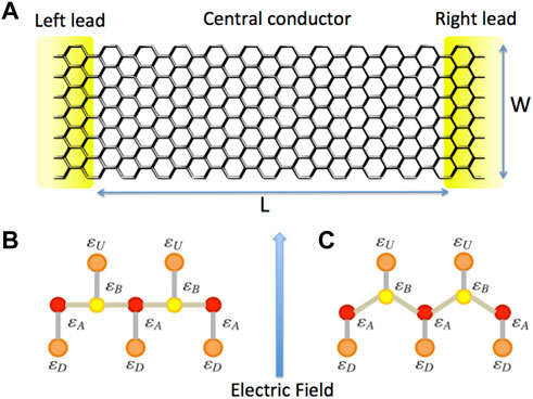
FIGURE 1. (A) Schematic view of the considered ASNR, (B) and (C) side view of the planar (α = 0) and the non-planar (α ≠ 0) Silicene nanostructures. In this panel, ɛ(U,D) represents the on-site energy of the ad-atoms pinned at the A(B) ribbon sites.
To analyze the thermoelectric behavior of the doped A-SNR, we have adopted the linear response approximation, in which an effective voltage drop ΔV and a temperature difference ΔT are applied between the left and right contacts. Within this approach, the electronic current Ie and the heat current IQ are given by
where e is the electron charge, T is the absolute temperature, and Kn (with n = 0, 1, 2) is the thermal integral defined as
Here, h is the Planck constant, μ is the chemical potential, f (ɛ, T) is the equilibrium Fermi–Dirac distribution, and
The electronic conductance is defined as G = −Ie/ΔV, and it can be obtained directly from Equation 3.
The Seebeck coefficient S is calculated in the linear response regime, namely, |ΔT| ≪ T and |eΔV| ≪ μ. It is defined as the voltage drop induced by a temperature gradient at zero electric current, S = ΔV/ΔT|Ie = 0 [Eq. 3], in the limit ΔT → 0. Thus,
The electron contribution to the thermal conductance is defined as the ratio between the thermal current IQ and the temperature gradient ΔT when the electric current Ie is zero,
Finally, we have calculated the Lorenz number for the considered heterostructures, which is defined as
where σ is the electronic conductivity and T is the temperature of the system. For metals, this relation remains constant, with a value of
We have analytically determined the transmission function of the system as a function of the energy. For this purpose, we have used an effective model in which the nanoribbon is mapped into a one-dimensional diatomic chain (See the Supplementary Material). Thus, the total transmission
Considering
In the aforementioned equations, we have considered the following definitions:
where kc and k are the wavenumbers in the effective one-dimensional chain, θc and θ are phases between the A(B) atoms in the ribbons, and qm is the discrete electronic wavenumber obtained by imposing the hard-wall boundary condition to the ribbon width. In armchair nanoribbons qm = mπ/(M+1), with m = 1, 2, …, M, which corresponds to the number of transverse energy channels available in the ribbon.
The results for the transmission function
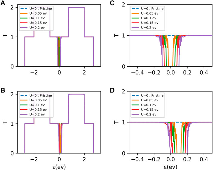
FIGURE 2. Transmission vs. Fermi energy for an A-SNR of width N = 5 and length L =80 for several external potential intensities, considering two different on-site energies for the ad-atoms. In (A) ɛ0 = 0 and (B) ɛ0 = 0.1γ. In both panels, the pristine N = 5 A-SNR has been included as references (dashed blue line). Panels (C) and (D) are zoomed in to the region of interest (around the energy of the ad-atoms). All curves were made considering α = 0.1.
The results for the electronic conductance G and the Seebeck coefficient S for a N = 5 A-SNR, of length L = 80 and α = .1, for different potential intensities U and different temperatures are exhibited in Figure 3 (a) and (c). To analyze the case of an impurity other than a silicon atom of the ribbon, we have chosen the ad-atom energy ɛ0 = 0.1 γ. At room temperature (300K), it is possible to observe that U strongly affects the behavior of G, progressively generating a conductance gap for U values greater than 0.1 eV. It is a consequence of the
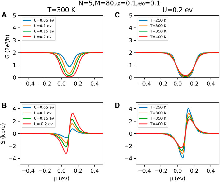
FIGURE 3. Electronic conductance and thermopower for an A-SNR of width N = 5 and length L = 80. In panels (A) and (B), we have fixed the temperature in 300K, and then variations of the external potential intensity, whereas in panels (C) and (D), we have considered variations of the temperature of the heterostructure.
On the other hand, in Figure 3B, we show that the Seebeck coefficient S presents a crescent value of its maximum as the external potential U increases. This behavior is a direct consequence of the noisy and asymmetric curves of transmission
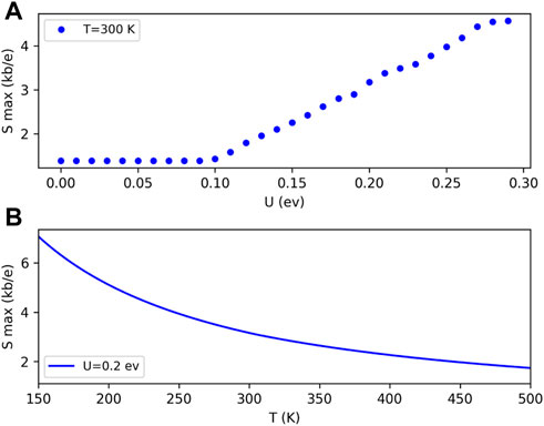
FIGURE 4. Maximum of the Seebeck coefficient behavior (Smax) as a function of (A) external potential intensity for room temperature and (B) temperature, for a fixed external potential U.
The results for the electronic conductance, the electronic thermal conductance, and the Lorenz number for a N = 5 A-SNR of length L = 80 and α = 0.1, for different potential intensities U and different temperatures T, are exhibited in Figure 5. In these plots, it is possible to observe that the electronic thermal conductance κel is affected by the variations of U and T [panels (b) and (e), respectively], reducing its value around the ad-atom energy (ɛ0 = 0.1 γ) and generating a gap behavior that differs with respect to the conductance curves [panels (a) and (d)]. The κel gap becomes broader and softens compared to the G gap. In addition, for different values of the external potential U and temperatures T and just at the ad-atom energy, κel exhibits an increase from the thermal integrals’ behavior K0, K1, and K2 at this energy. Thus, if we considered the Sommerfeld expansion of these integrals, the dominant terms in the definition of κel will be quadratic in the transmission function derivative and on the energy so that
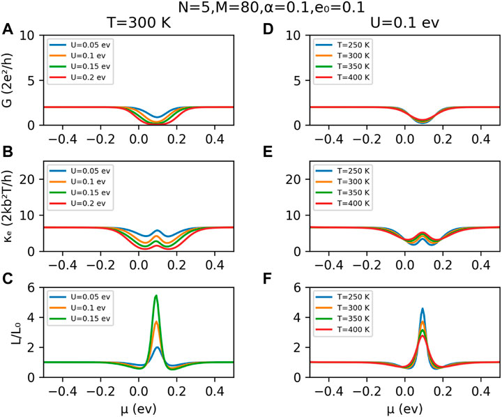
FIGURE 5. Electronic conductance, electronic thermal conductance, and Lorenz number for an A-SNR of width N = 5 and length L = 80. We have plotted panels (A), (B), and (C) for room temperature, increasing the external potential intensity. In panels (D), (E), and (F), we have considered variations of the temperature of the system.
In this context, by using the definition given in Eq. 9, we have calculated the Lorenz number
In order to estimate the thermoelectrical efficiency of the proposed system, we present results for the electronic figure of merit ZTel = TS2G/κel, which are displayed in Figure 6. For these calculations, we have not considered the phonon contribution to the thermal conductance because it is well-known that in narrow pristine A-SNR, κph ≤ κel [see Pan et al. [14] for a complete analysis of these quantities]. In this sense, we expect that the ad-atoms in the central conductor would reduce even more the lattice contribution to the total thermal conductance of the system κ. As it is observed in both panels of Figure 6, as the external potential intensity is increased, the thermal efficiency becomes better. In addition, as the temperature is increased, the maximum of ZTel tends to reduce its magnitude. Both results are a direct consequence of the Seebeck coefficient behavior as a function of the external potential and the temperature, as it is shown in Figure 3 and Figure 4. The electronic figure of merit depends quadratically on S; therefore, any abrupt change on this thermal quantity strongly affects the thermoelectrical efficiency of the proposed system.
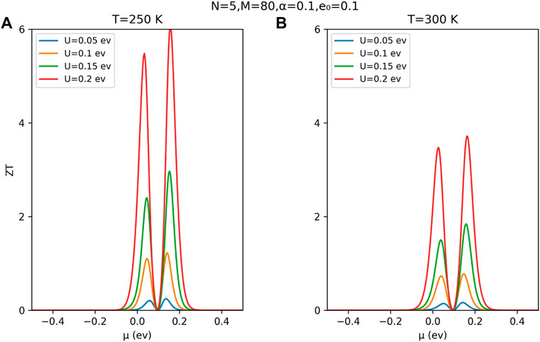
FIGURE 6. Electronic figure of merit as a function of the chemical potential, for an A-SNR of width N = 5 and length L = 80. We have plotted panels (A) and (B) for two different temperatures, increasing the external potential intensity.
In this work, we have studied the thermoelectrical properties of armchair silicene nanoribbon heterostructures. Using an effective one-dimensional model, we have determined the electron transmission function of the system analytically. With this result, we have calculated and analyzed the behavior of the electronic conductance, the Seebeck coefficient, and the electronic contribution to the thermal conductance as a function of an external potential intensity and the temperature. We have obtained a controlled tuning of the Seebeck coefficient maximum Smax at room temperature as the external potential U is modified. This behavior is explained by the abrupt changes in the transmission function around the electronic gap produced by the ad-atoms. Furthermore, as expected, as the system’s temperature increases, Smax decreases because the transmission changes become smooth, especially for temperatures above 300K.
In the case of electronic thermal conductance, we have obtained a reduction of its magnitude around the ad-atom energy as U increases. However, this reduction is less than that obtained for the electronic conductance at the same energy range. Therefore, we have obtained a violation of the classical Wiedemann–Franz law, reflected in the Lorenz number behavior, which presents a clear dependence on the external potential intensity U and the temperature of the system.
It is important to mention that the obtained thermoelectric efficiency only considers the electronic contribution to the thermal conductance. Independently that we expect a strong reduction to the phonon mean free path due to the presence of the ad-atoms, the lattice contribution to the thermal conductance will not be zero; therefore, the total figure of merit should be less than that of our results but still better in comparison with the pristine case.
The thermoelectric behavior described in this work is quite general for the considered heterostructures. We have obtained similar results for different geometrical configurations, considering variations in the width and length of the conductor region. In this sense, we have focused on the simplest system to give a better physical understanding of the thermoelectrical phenomena present in these nanostructures.
The raw data supporting the conclusion of this article will be made available by the authors, without undue reservation.
KG and CN performed the analytic and numerical calculation. PO and LR conceived the study. All authors wrote and contributed to the final version of the manuscript and approved the submission.
This work was financially supported by FONDECYT (grant numbers: 1220700 and 1201876).
The authors declare that the research was conducted in the absence of any commercial or financial relationships that could be construed as a potential conflict of interest.
All claims expressed in this article are solely those of the authors and do not necessarily represent those of their affiliated organizations, or those of the publisher, the editors, and the reviewers. Any product that may be evaluated in this article, or claim that may be made by its manufacturer, is not guaranteed or endorsed by the publisher.
Supplementary Material for this article can be found online at: https://www.frontiersin.org/articles/10.3389/fphy.2022.1091325/full#supplementary-material
2. Gayner C, Kar KK. Recent advances in thermoelectric materials. Prog Mater Sci (2016) 83:330–82. doi:10.1016/j.pmatsci.2016.07.002
3. Hicks LD, Dresselhaus MS. Thermoelectric figure of merit of a one-dimensional conductor. Phys Rev B (1993) 47:16631–4. doi:10.1103/physrevb.47.16631
4. Khitun A, Balandin A, Liu JL, Wang KL. In-plane lattice thermal conductivity of a quantum-dot superlattice. J Appl Phys (2000) 88:696–9. doi:10.1063/1.373723
5. Balandin AA, Lazarenkova OL. Mechanism for thermoelectric figure-of-merit enhancement in regimented quantum dot superlattices. Appl Phys Lett (2003) 82:415–7. doi:10.1063/1.1539905
6. Sadeghi H, Sangtarash S, Lambert CJ. Enhancing the thermoelectric figure of merit in engineered graphene nanoribbons. Beilstein J Nanotechnol (2015) 6:1176–82. doi:10.3762/bjnano.6.119
7. Venkatasubramanian R, Siivola E, Colpitts T, O’Quinn B. Thin-film thermoelectric devices with high room-temperature figures of merit. Nature (London) (2001) 413:597–602. doi:10.1038/35098012
8. Harman TC, Taylor PJ, Walsh MP, LaForge BE. Quantum dot superlattice thermoelectric materials and devices. Science (2002) 297:2229–32. doi:10.1126/science.1072886
9. Hochbaum AI, Chen R, Delgado RD, Liang W, Garnett EC, Najarian M, et al. Enhanced thermoelectric performance of rough silicon nanowires. Nature (London) (2008) 451:163–7. doi:10.1038/nature06381
10. Boukai AI, Bunimovich Y, Tahir-Kheli J, Yu J-K, Goddard WA, Heath JR. Silicon nanowires as efficient thermoelectric materials. Nature (London) (2008) 451:168–71. doi:10.1038/nature06458
11. Chen X-K, Chen K-Q. Thermal transport of carbon nanomaterials. J Phys Condensed Matter (2020) 32:153002. doi:10.1088/1361-648x/ab5e57
12. Wu D, Cao X, Jia P, Zeng YJ, Feng YX, Tang LM, et al. Excellent thermoelectric performance in weak coupling molecular junctions with electrode doping and electrochemical gating. Sci China Phys Mech Astron (2020) 63:276811. doi:10.1007/s11433-019-1528-y
13. Zberecki K, Wierzbicki M, Barnaś J, Swirkowicz R. Thermoelectric effects in silicene nanoribbons. Phys Rev B (2013) 88:115404. doi:10.1103/physrevb.88.115404
14. Pan L, Liu HJ, Tan XJ, Lv HY, Shi J, Tang XF, et al. Thermoelectric properties of armchair and zigzag silicene nanoribbons. Phys Chem Chem Phys (2012) 14:13588–93. doi:10.1039/C2CP42645E
15. Li H-P, Zhang R. Vacancy-defect–induced diminution of thermal conductivity in silicene. EPL (Europhys. Lett.) (2012) 99:36001. doi:10.1209/0295-5075/99/36001
16. Aufray B, Kara A, Vizzini S, Oughaddou H, Léandri C, Ealet B, et al. Graphene-like silicon nanoribbons on ag(110): A possible formation of silicene. Appl Phys Lett (2010) 96:183102. doi:10.1063/1.3419932
17. Lalmi B, Oughaddou H, Enriquez H, Kara A, Vizzini S, Ealet B, et al. Epitaxial growth of a silicene sheet. Appl Phys Lett (2010) 97:223109. doi:10.1063/1.3524215
18. Mahan GD, Sofo JO. The best thermoelectric. Proc Natl Acad Sci USA (1996) 93:7436–9. doi:10.1073/pnas.93.15.7436
19. Gómez-Silva G, Ávalos-Ovando O, Ladrón de Guevara ML, Orellana PA. Enhancement of thermoelectric efficiency and violation of the Wiedemann-Franz law due to Fano effect. J Appl Phys (2012) 111:053704. doi:10.1063/1.3689817
20. Zheng J, Zhu M-J, Chi F. Fano effect on the thermoelectric efficiency in parallel-coupled double quantum dots. J Low Temp Phys (2012) 166:208–17. doi:10.1007/s10909-011-0417-2
21. García-Suárez VM, Ferradás R, Ferrer J. Impact of Fano and Breit-Wigner resonances in the thermoelectric properties of nanoscale junctions. Phys Rev B (2013) 88:235417. doi:10.1103/physrevb.88.235417
22. Fu H-H, Gu L, Wu D-D, Zhang Z-Q. Enhancement of the thermoelectric figure of merit in DNA-like systems induced by Fano and Dicke effects. Phys Chem Chem Phys (2015) 17:11077–87. doi:10.1039/c4cp04382k
23. Sierra MA, Saiz-Bretín M, Domínguez-Adame F, Sánchez D. Interactions and thermoelectric effects in a parallel-coupled double quantum dot. Phys Rev B (2016) 93:235452. doi:10.1103/physrevb.93.235452
24. Wang R-N, Dong G-Y, Wang S-F, Fu G-S, Wang J-L. Impact of contact couplings on thermoelectric properties of anti, Fano, and Breit-Wigner resonant junctions. J Appl Phys (2016) 120:184303. doi:10.1063/1.4967751
Keywords: silicene nanoribbons, thermoelectric, Seebeck coefficient, conductance, tight-binding
Citation: González KA, Núñez CD, Orellana PA and Rosales L (2023) Tuning the thermoelectric properties of doped silicene nanoribbon heterostructures. Front. Phys. 10:1091325. doi: 10.3389/fphy.2022.1091325
Received: 06 November 2022; Accepted: 23 December 2022;
Published: 16 February 2023.
Edited by:
Judith Helena Ojeda Silva, Universidad Pedagógica y Tecnológica de Colombia, ColombiaCopyright © 2023 González, Núñez, Orellana and Rosales. This is an open-access article distributed under the terms of the Creative Commons Attribution License (CC BY). The use, distribution or reproduction in other forums is permitted, provided the original author(s) and the copyright owner(s) are credited and that the original publication in this journal is cited, in accordance with accepted academic practice. No use, distribution or reproduction is permitted which does not comply with these terms.
*Correspondence: L. Rosales, bHVpcy5yb3NhbGVzYUB1c20uY2w=
Disclaimer: All claims expressed in this article are solely those of the authors and do not necessarily represent those of their affiliated organizations, or those of the publisher, the editors and the reviewers. Any product that may be evaluated in this article or claim that may be made by its manufacturer is not guaranteed or endorsed by the publisher.
Research integrity at Frontiers

Learn more about the work of our research integrity team to safeguard the quality of each article we publish.