 Xiuyu Wang1
 Min Kang
 Yue Su
 Xurui Mao
- 1School of Microelectronics, Tianjin University, Tianjin, China
- 2Beijing Institute of Spacecraft System Engineering, Beijing, China
- 3Institute of Semiconductors, Chinese Academy of Sciences, Beijing, China
A self-powered IoT system with high integration, robust performance, and adaptability to complex environments is one of the current research hotspots. Piezoelectric materials have been widely used in pressure sensing and energy harvesting due to their stable output electrical properties. In this paper, a heterogeneous integrated self-powered IoT system based on a lithium niobate (LiNbO3) piezoelectric device and CMOS readout circuit is proposed. The piezoelectric sensor is fabricated by depositing electrodes on the surface of the 36°Y-cut LiNbO3 piezoelectric material. The sensitivity of the fabricated sensor is 17.5 mV/kPa. Based on the CSMC 0.18 μm BCD process, a ring voltage-controlled oscillator (VCO) based on the current starvation delay element is designed as a wireless data transmission unit. The oscillator has two tuning terminals, which can realize frequency alignment and voltage threshold judgment. Using photolithography, wire bonding technology, etc., the heterogeneous integration of the Si-based chip and LiNbO3 piezoelectric device is realized. The experimental results show that below 1.8 V supply voltage, the oscillation frequency of the chip increases with the increase in the control terminal voltage, which provides an idea for solving the energy supply problem of an IoT system. This system has great application potential in the field of self-powered sensing.
1 Introduction
With the advent of the Internet of Things (IoT) era, sensor networks have gradually become a research hotspot. The traditional wired sensor network has the advantages of fast transmission rate and good robustness [1]. However, the power supply problem and existence of external wires limit its application in industrial, medical [2] and other fields. Therefore, wireless sensor networks are favored by researchers. At present, most wireless sensor systems require external power supply, while traditional batteries are bulky, short-lived and pollute the environment. An effective way to solve this problem is to obtain energy from nature, such as solar energy [3, 4], biological mechanical energy [5-7], ocean energy [8, 9], and convert it into electrical energy to achieve the self-powered IoT system [10, 11].
At present, energy harvesters based on the pyroelectric effect [12, 13] and photovoltaic effect [14] have been proposed, but their application scenarios are limited. The energy-harvesting system based on the triboelectric effect has also been widely used [15-17], although it has good output performance, but the output stability is poor. Since the piezoelectric effect was discovered in 1880, piezoelectric materials have been widely used in industrial, medical, military and other fields [18-20]. Based on the positive piezoelectric effect, piezoelectric materials can convert mechanical energy into electrical energy to drive electronic devices [21]. Since its charge is generated due to the asymmetry of the positive and negative charge centers inside the material, it has stable output performance. However, the electromechanical conversion efficiency of piezoelectric materials is low, while the power consumption of electronic devices is high. Technical solutions such as increasing the output power of piezoelectric devices [22-24] and reducing the power consumption of external readout circuits [25, 26] provide ideas for realizing self-powered supply for IoT systems, exploring applications in the human–computer interaction, health monitoring, and other fields. In addition, heterogeneous integration of piezoelectric devices with active electronic devices will contribute to more efficient, reliable, and portable self-powered IoT systems [27].
In this work, a heterogeneous integrated self-powered IoT system based on the LiNbO3 piezoelectric device and low power CMOS readout circuit is introduced. The LiNbO3 crystal is a good piezoelectric crystal with a small temperature coefficient, high electromechanical coupling coefficient, and stable performance. In this paper, the LiNbO3 crystal is used as a piezoelectric material. In addition, a current-starved voltage-controlled oscillator (VCO) with low power consumption is designed in this paper. The circuit is implemented using the CSMC 0.18 μm BCD process. The designed ring VCO consumes 8.67 μW and has a center frequency of 13.56 MHz. It belongs to the ISM band and can be used to send information in a wireless way.
2 Design of the self-powered IoT system
2.1 System structure
The heterogeneous integrated self-powered IoT system proposed in this paper is composed of an LiNbO3 piezoelectric device, voltage-doubling rectifier, and wireless transmission unit, as shown in Figure 1. The LiNbO3 device has two functions: one is to convert external mechanical energy into electrical energy by rectifying and the other is to supply power for the wireless transmission unit; in addition, as a sensor, the output piezoelectric signal is connected to the wireless transmission unit, and frequency tuning can be performed. The wireless transmission unit is a ring VCO with dual-tuned terminals, which has low power consumption compared to the LC VCO.
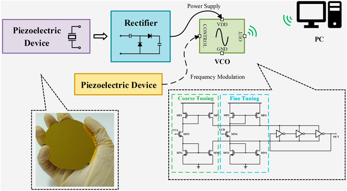
FIGURE 1. Structure diagram of the heterogeneous integrated self-powered IoT system. The piezoelectric device realizes energy harvesting through the rectifier and supplies power to the VCO, and the piezoelectric device is connected to the control terminal of the VCO to realize frequency modulation.
2.2 Piezoelectric device
When a pressure is applied to a piezoelectric material, the piezoelectric effect can be described by the piezoelectric constitutive equation:
where δ is the strain, T is the stress, D is the electrical displacement, E is the electric field strength, S is the elastic modulus, ɛ is the dielectric constant, and d is the piezoelectric coefficient.
Piezoelectric crystals grow in long-range order, according to the crystal space lattice, and have no symmetry center, so they have piezoelectricity. As shown in Figure 2, the LiNbO3 crystal is a trigonal crystal system at room temperature, which has the advantages of high Curie temperature [28] and strong piezoelectric and ferroelectric performances, and is widely used in the production of SAW devices, piezoelectric filters, transducers, laser modulators, etc. The LiNbO3 crystal is anisotropic, and the piezoelectric effect is the strongest in the direction of 38.9°, that is, d22 is the largest at this time [29]. The commercial LiNbO3 crystal cutting direction close to it is 36°Y-cut. In this work, piezoelectric devices were fabricated by depositing Ti/Au on the surface of the 36°Y-cut LiNbO3 piezoelectric crystal. When the piezoelectric device is pressed, positive charge is generated on one surface of the device, and correspondingly, a negative charge is generated on the other surface. Since the impedance of the external circuit is not infinite, electrons flow from one electrode to the other through the external circuit.
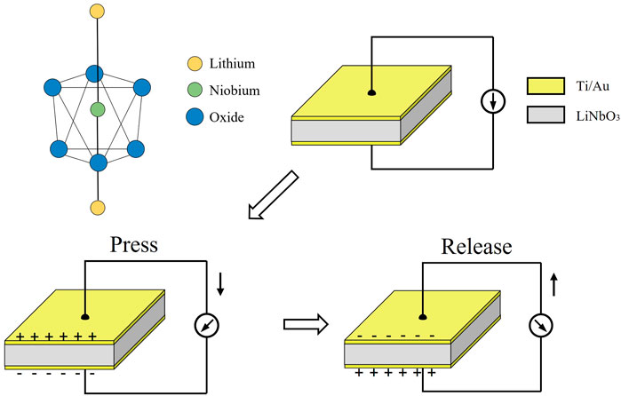
FIGURE 2. LiNbO3 lattice structure and diagrams of internal and surface charges under pressure and release.
2.3 Wireless transmission unit
Usually, for the VCO, the change of voltage of the power supply and the control terminal will cause the frequency jitter. When the power supply voltage is stable, the LC VCO shows a sensitive frequency response to the change of the control terminal voltage, and it has less phase noise. However, the power consumption and area are also increased. For the self-powered IoT system, both frequency stability and power consumption need to be considered. Based on the low-power design requirements of the self-powered system, the wireless transmission unit uses a current-starved ring VCO to convert the pressure information on the sensor into frequency information and send it wirelessly. Current-starved ring oscillators control the frequency of oscillation by supplying current to the oscillator by mirroring the bias current. The delay time of a current-starved delay element can be expressed as [30]
where CL is the load capacitance, VDD is the supply voltage, K is the process parameters of transistors, VC is the control voltage, and VTH is the threshold voltage.
The frequency of the ring oscillator is related to the delay time of each inverter and the number of inverter stages, and the oscillation frequency can be expressed by the following formula:
where N is the number of inverter stages and td is the delay time of each stage of the inverter. In order to reduce the power consumption of the system, the current of the three-stage inverter comes from the bias current source, and the operating frequency of the oscillator is reduced as well Tran and Dang [31]. The schematic of the oscillator is shown in Figure 3. The oscillator has two control terminals, which realize coarse tuning and fine tuning. The coarse-tuning terminal is used to stabilize the output frequency at the ISM frequency band. When the output reaches a certain threshold, the oscillator circuit is turned on and oscillates in a specific frequency band. The fine-tuning terminal is associated with voltage detection, which can change the frequency of the oscillator within a specific frequency band. Piezoelectric devices can be equivalent to a voltage source in series with a capacitor or a charge source in parallel with the capacitor. The gate resistance of the MOS transistor is large. According to the piezoelectric equivalent circuit, the piezoelectric element is connected to the gate of the transistor. At this time, the external load impedance is large, so the conversion of the charge signal can be realized. The stress condition can be characterized by the frequency and the output time. The designed chip has a low power consumption of 8.676 μW with a VDD of 1.8 V.
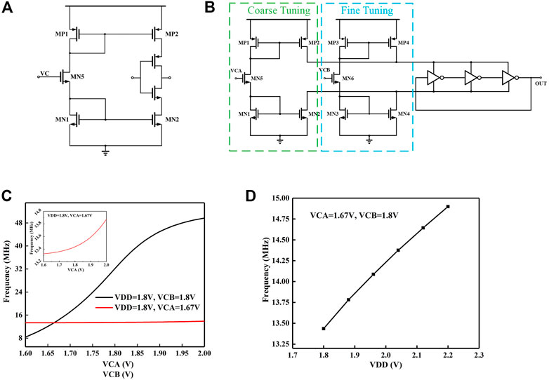
FIGURE 3. Low-power wireless information-sending unit. (A) Schematic of the current-starved delay element; (B) schematic of the low-power current-starved ring oscillator, and the circuit has coarse- and fine-tuning functions to achieve frequency alignment and threshold judgment, respectively; (C) simulation of the variation curve of oscillation frequency with VCA and VCB; and (D) simulation of the variation curve of oscillation frequency with VDD.
Figures 3C,D show the correspondence between oscillator frequency and VDD, VCA, and VCB. From Figure 3C, it can be concluded that the change of the output frequency is sensitive to the change of the coarse-tuning terminal VCA. In this paper, VCA is set to 1.67 V, and the corresponding output frequency is about 13.56 MHz. For VCB, the frequency variation range is 13.32–13.87 MHz, which belongs to the ISM frequency band, and the wireless sensor unit can transmit information wirelessly in this frequency band. As analyzed previously, the delay of each stage of the inverter is also related to VDD. As shown in Figure 3D, when VDD varies from 1.8 to 2.2 V, the output frequency changes from 13.44 to 14.90 MHz.
3 Results and discussion
The test environment for the electrical performance of the piezoelectric device is shown in Figure 4A. The piezoelectric device is subjected to pressure by a stepper motor, and the corresponding signal is collected using an electrometer (Keithley, 6514). The stepping motor is controlled using special software on the computer, and the pressure can be read out using the dynamometer (HANDPI, HP-500). The effective area of the sensor is 0.5 cm2. Figures 4B,C show the change of open circuit voltage and charge of piezoelectric devices with time in the pressure range of 10–700 kPa. Both the output voltage and the charge increase with pressure. It is because the increase in pressure causes an increase in the electric dipole moment, creating a larger potential difference between the top and bottom electrodes. The sensor has robust output performance, and the sensitivity of the sensor is up to 17.5 mV/kPa, which can meet the need of wireless sensing.
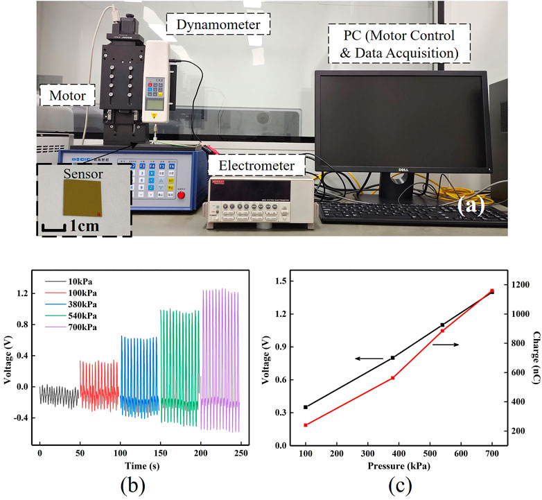
FIGURE 4. (A) Test environment of the LiNbO3 piezoelectric sensor; (B) open-circuit voltage of the sensor under different pressures; and (C) open-circuit voltage and charge of the sensor under different pressures.
The PCB test board of the chip is shown in Figure 5A. For the convenience of welding and testing, the chip is packaged in a QFN24 case. Figure 5B shows the curve of the oscillator output frequency as a function of VCA when VCA = 1.8 V and VDD = 1.8, 1.9, and 2.0 V. As VDD increases, the corresponding output frequency also increases. In addition, as shown in Figure 5C, we compared the test results and simulation results when VDD = 1.8 V and VCA = 1.8 V. Due to the existence of parasitic capacitances such as PCB and QFN cases, the frequency of chip testing is lower than that of simulation under the same conditions. As shown in Figure 5D, the 2.2-μF capacitor can be charged to 2.03 V within 50 s when pressed by the human hand. At this time, the energy stored in the capacitor is Eenergy = 4.53 μJ. The power consumption of the oscillator is 8.67 μW, and the start-up time is only 191 ns, so it is enough to drive the oscillator. The results show that the heterogeneous integrated IoT system can collect the energy of the piezoelectric device, supply power to the chip within a certain period of time, and realize the reading of pressure information within this period.
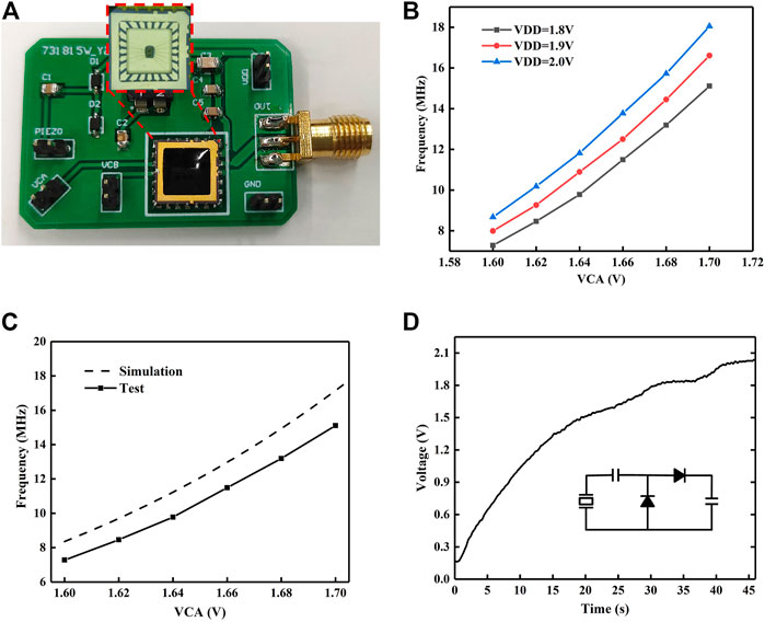
FIGURE 5. Low-power wireless transmit unit tests. (A) PCB test board for the chip; (B) test for the variation curve of oscillation frequency with VDD; (C) comparison of simulation and test results of output frequency variation with VCA; and (D) charging of the capacitor as the device is pressed and released by the human hand.
4 Method for heterogeneous integration of piezoelectric devices and Si-based integrated circuits
In order to improve the integration of the heterogeneous integrated IoT system, a part of the area on the LiNbO3 substrate is reserved as the active area in this work. This area integrates the voltage-doubling rectifier and the wireless transmission unit, and the other area is the Ti/Au electrode, which is used to extract the piezoelectric charge. The process and explosion diagram of the heterogeneous integrated sensing unit are shown in Figure 6, and the detailed steps are as follows: preparing the LiNbO3 substrate; spin-coating the negative photoresist (AR-N 4340) on the top surface of the LiNbO3 substrate, for which the speed and corresponding time are 1,000 rpm for 6 s and then 6,000 rpm for 20 s; prebaking for 2 min at 110°C; exposing for 40 s; post-baking for 4 min at 105°C; developing for 1 min; depositing Ti/Au electrodes for 20/200 nm on the top and bottom surfaces of LiNbO3; and soaking in acetone to remove the photoresist. Then, through wire bonding, reflow soldering, etc., the Si-based chip is fixed on the surface of the wafer and coated with silica gel for protection.
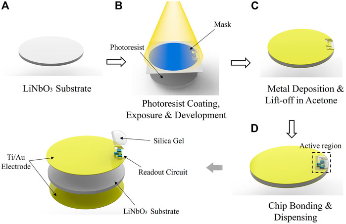
FIGURE 6. Method for heterogeneous integration of piezoelectric devices and Si-based integrated circuits. (A) substrate preparing; (B) photoresist coating, exposure and development; (C) metal deposition & lift-off in acetone; (D) chip bonding and dispensing.
Inspired by the PCB, for the active area reserved in the heterogeneous integrated IoT system, part of the metal on the surface of the wafer is used as wiring by designing the pattern to realize the interconnection of components. It is worth noting that for the convenience of wiring, the bottom surface of the integrated unit is considered the positive electrode of the piezoelectric device, and the top surface is considered the negative electrode.
5 Conclusion
In conclusion, a heterogeneous integrated self-powered IoT system based on the LiNbO3 piezoelectric material and CMOS readout circuit is proposed in this work. An LiNbO3 piezoelectric sensor was fabricated by vapor-depositing electrodes on the surface of the LiNbO3 piezoelectric material. The charge that the piezoelectric device can generate is 1,160 nC under the pressure of 700 kPa. The sensitivity of the sensor is up to 17.5 mV/kPa, which can meet the need of wireless sensing. Based on the CSMC 0.18 μm BCD process, a low-power VCO circuit was designed with a power consumption of 8.67 μW and can work in the 13.56 MHz ISM frequency band. Through lithography and other processes, the designed low-power chip is heterogeneously integrated with the LiNbO3 piezoelectric material. This system can send data at regular intervals. It has significant advantages in high integration, high anti-interference, etc., which provides methods for the energy supply problem of an IoT system.
Data availability statement
The original contributions presented in the study are included in the article/Supplementary Material; further inquiries can be directed to the corresponding authors.
Author contributions
XW planned the experiment. MK designed the chip and completed the relevant tests. YZ provided the design plan. YS provided the packaging process guidance. XZ provided the experimental key technology, and XM instructed the chip design and experiment.
Funding
This work was supported in part by the National Natural Science Foundation of China under Grants 61874104 and 11673019 and in part by the 2021 Special Research Assistant Project Funding E27T01HZ01.
Conflict of interest
The authors declare that the research was conducted in the absence of any commercial or financial relationships that could be construed as a potential conflict of interest.
Publisher’s note
All claims expressed in this article are solely those of the authors and do not necessarily represent those of their affiliated organizations, or those of the publisher, the editors, and the reviewers. Any product that may be evaluated in this article, or claim that may be made by its manufacturer, is not guaranteed or endorsed by the publisher.
References
1. Abdulkarem M, Samsudin K, Rokhani FZ, A Rasid MF. Wireless sensor network for structural health monitoring: A contemporary review of technologies, challenges, and future direction. Struct Health Monit (2020) 19:693–735. doi:10.1177/1475921719854528
2. Liu K, Chen H, Wang Y, Wang M, Tang J. Wearable flexible phototherapy device for knee osteoarthritis. Electronics (2021) 10:1891. doi:10.3390/electronics10161891
3. Bouguera T, Diouris J-F, Andrieux G, Chaillout J-J, Jaouadi R. A novel solar energy predictor for communicating sensors. IET Commun (2018) 12:2145–9. doi:10.1049/iet-com.2018.5244
4. Luo P, Peng D, Wang Y, Zheng X. Review of solar energy harvesting for iot applications. In: Proceeding of the 2018 IEEE Asia Pacific Conference on Circuits and Systems (APCCAS); 2018 October 26–30; Chengdu, China. IEEE (2018). p. 512–5.
5. Ding N, Deng F, Cai Y, Gui P, Fan X. Wearable human foot mechanical energy harvesting device based on moving-coil generator. In: Proceeding of the 2019 Chinese Control Conference (CCC); 2019 July 27–30; Guangzhou, China. IEEE (2019). p. 6498–503.
6. Catacuzzeno L, Orfei F, Di Michele A, Sforna L, Franciolini F, Gammaitoni L. Energy harvesting from a bio cell. Nano Energy (2019) 56:823–7. doi:10.1016/j.nanoen.2018.12.023
7. Xie LH, Du R. Harvesting human biomechanical energy to power portable electronics. Adv Mat Res (2012) 516:1779–84. doi:10.4028/www.scientific.net/amr.516-517.1779
8. Li Z, Yang D, Zhang Z, Lin S, Cao B, Wang L, et al. A droplet-based electricity generator for large-scale raindrop energy harvesting. Nano Energy (2022) 100:107443. doi:10.1016/j.nanoen.2022.107443
9. Nabavi SF, Farshidianfar A, Afsharfard A. Novel piezoelectric-based ocean wave energy harvesting from offshore buoys. Appl Ocean Res (2018) 76:174–83. doi:10.1016/j.apor.2018.05.005
10. Wu Z, Cheng T, Wang ZL. Self-powered sensors and systems based on nanogenerators. Sensors (2020) 20:2925. doi:10.3390/s20102925
11. Garg N, Garg R. Multi-source energy harvesting system for sensor nodes. In: Proceeding of the International Conference on Advanced Informatics for Computing Research; 2018 July 14-15; Shimla, India. Springer (2018). p. 282–93.
12. Jaziri N, Boughamoura A, Müller J, Mezghani B, Tounsi F, Ismail M. A comprehensive review of thermoelectric generators: Technologies and common applications. Energ Rep (2020) 6:264–87. doi:10.1016/j.egyr.2019.12.011
13. Ryu H, Kim S-W. Emerging pyroelectric nanogenerators to convert thermal energy into electrical energy. Small (2021) 17:1903469. doi:10.1002/smll.201903469
14. Pozo B, Garate JI, Araujo JÁ, Ferreiro S. Photovoltaic energy harvesting system adapted for different environmental operation conditions: Analysis, modeling, simulation and selection of devices. Sensors (2019) 19:1578. doi:10.3390/s19071578
15. Chen H, Lu Q, Cao X, Wang N, Wang ZL. Natural polymers based triboelectric nanogenerator for harvesting biomechanical energy and monitoring human motion. Nano Res (2022) 15:2505–11. doi:10.1007/s12274-021-3764-6
16. Yuan W, Zhang C, Zhang B, Wei X, Yang O, Liu Y, et al. Wearable, breathable and waterproof triboelectric nanogenerators for harvesting human motion and raindrop energy. Adv Mater Technol (2022) 7:2101139. doi:10.1002/admt.202101139
17. Luo J, Wang Z, Xu L, Wang AC, Han K, Jiang T, et al. Flexible and durable wood-based triboelectric nanogenerators for self-powered sensing in athletic big data analytics. Nat Commun (2019) 10:5147–9. doi:10.1038/s41467-019-13166-6
18. Yang L, Kong X, Li F, Hao H, Cheng Z, Liu H, et al. Perovskite lead-free dielectrics for energy storage applications. Prog Mater Sci (2019) 102:72–108. doi:10.1016/j.pmatsci.2018.12.005
19. Chorsi MT, Curry EJ, Chorsi HT, Das R, Baroody J, Purohit PK, et al. Piezoelectric biomaterials for sensors and actuators. Adv Mater (2019) 31:1802084. doi:10.1002/adma.201802084
20. Han M, Wang H, Yang Y, Liang C, Bai W, Yan Z, et al. Three-dimensional piezoelectric polymer microsystems for vibrational energy harvesting, robotic interfaces and biomedical implants. Nat Electron (2019) 2:26–35. doi:10.1038/s41928-018-0189-7
21. Safaei M, Sodano HA, Anton SR. A review of energy harvesting using piezoelectric materials: State-of-the-art a decade later (2008–2018). Smart Mater Struct (2019) 28:113001. doi:10.1088/1361-665x/ab36e4
22. Wang Y, Xu M, Zhang F, Wang Y, Zhang L, Zhang Q, et al. Design on orientation of one-dimensional zno/p (vdf-hfp) nanocomposites for significant enhanced electromechanical conversion. Composites Sci Tech (2021) 204:108635. doi:10.1016/j.compscitech.2020.108635
23. Deng W, Yang T, Jin L, Yan C, Huang H, Chu X, et al. Cowpea-structured pvdf/zno nanofibers based flexible self-powered piezoelectric bending motion sensor towards remote control of gestures. Nano Energy (2019) 55:516–25. doi:10.1016/j.nanoen.2018.10.049
24. Shuai C, Liu G, Yang Y, Qi F, Peng S, Yang W, et al. A strawberry-like ag-decorated barium titanate enhances piezoelectric and antibacterial activities of polymer scaffold. Nano Energy (2020) 74:104825. doi:10.1016/j.nanoen.2020.104825
25. Nazemi H, Antony Balasingam J, Swaminathan S, Ambrose K, Nathani MU, Ahmadi T, et al. Mass sensors based on capacitive and piezoelectric micromachined ultrasonic transducers—Cmut and pmut. Sensors (2020) 20:2010. doi:10.3390/s20072010
26. Kang S, Qian Z, Rajaram V, Calisgan SD, Rinaldi M. Chip-scale mems-cmos multispectral infrared chemical sensor. In: Proceeding of the 2019 IEEE 32nd International Conference on Micro Electro Mechanical Systems (MEMS); 2019 January 27–31; Seoul, South Korea. IEEE (2019). p. 133–6.
27. Shi C, Costa T, Elloian J, Shepard K. Monolithic integration of micron-scale piezoelectric materials with cmos for biomedical applications. In: Proceeding of the 2018 IEEE International Electron Devices Meeting (IEDM); 2018 December 1–5; San Francisco, CA. IEEE (2018). p. 4–5.
28. Smith R, Welsh F. Temperature dependence of the elastic, piezoelectric, and dielectric constants of lithium tantalate and lithium niobate. J Appl Phys (1971) 42:2219–30. doi:10.1063/1.1660528
29. Kawamata A, Hosaka H, Morita T. Non-hysteresis and perfect linear piezoelectric performance of a multilayered lithium niobate actuator. Sensors Actuators A: Phys (2007) 135:782–6. doi:10.1016/j.sna.2006.08.025
30. Jovanović GS, Stojčev MK. Current starved delay element with symmetric load. Int J Electron (2006) 93:167–75. doi:10.1080/00207210600560078
31. Tran DX, Dang TT. An ultra-low power consumption and very compact 1.49 ghz cmos voltage controlled ring oscillator. In: Proceeding of the 2014 International Conference on Advanced Technologies for Communications (ATC 2014); 2014 October 12–14; Vietnam Posts & Telecommunicat Inst Technol Hanoi, Hanoi, Vietnam. IEEE (2014). p. 239–44.
Keywords: heterogeneous integration, self-powered, wireless sensing, piezoelectric, LiNbO3
Citation: Wang X, Kang M, Zhao Y, Su Y, Zhang X and Mao X (2022) A heterogeneous integrated self-powered IoT system of an LiNbO3 device and CMOS readout circuit. Front. Phys. 10:1090769. doi: 10.3389/fphy.2022.1090769
Received: 06 November 2022; Accepted: 24 November 2022;
Published: 20 December 2022.
Edited by:
Chen Xu, Beijing University of Technology, ChinaReviewed by:
Huan Zhang, Beijing University of Technology, ChinaRongsheng Chen, South China University of Technology, China
Copyright © 2022 Wang, Kang, Zhao, Su, Zhang and Mao. This is an open-access article distributed under the terms of the Creative Commons Attribution License (CC BY). The use, distribution or reproduction in other forums is permitted, provided the original author(s) and the copyright owner(s) are credited and that the original publication in this journal is cited, in accordance with accepted academic practice. No use, distribution or reproduction is permitted which does not comply with these terms.
*Correspondence: Yang Zhao, YWJjMjcwOTc4NkAxMjYuY29t; Xurui Mao, bWFveHVydWlAc2VtaS5hYy5jbg==