 Beiju Huang
 Zanyun Zhang
 Meixin Li
 Kaixin Zhang
 Tianjun Liu
 Hao Jiang
 Qixin Wang
 Jiaming Xing
95% of researchers rate our articles as excellent or good
Learn more about the work of our research integrity team to safeguard the quality of each article we publish.
Find out more
ORIGINAL RESEARCH article
Front. Phys. , 15 December 2022
Sec. Optics and Photonics
Volume 10 - 2022 | https://doi.org/10.3389/fphy.2022.1079167
This article is part of the Research Topic Silicon-Based Optoelectronics and Microelectronics Integration Technology View all 7 articles
In this paper, a hybrid Mach-Zehnder optical modulator is proposed based on silicon nitride/organic polymer waveguides, which is expected to break through the performance bottleneck of the silicon-based optical modulator by exploiting the low-loss optical transmission property of silicon nitride waveguides and the excellent modulation performance of organic polymers. For reduction of the optical loss and ease of photonic packaging, perfectly vertical silicon nitride bidirectional grating couplers are utilized for both input/output optical coupling and power splitting/combining. Thus, a Mach-Zehnder interferometer can be constructed with a back-to-back configuration of such grating couplers. With grating apodization, the coupler can achieve a simulated coupling efficiency of 70%. To bridge the silicon nitride waveguides and the polymer waveguides, a longitudinal adiabatic mode-spot converter with a transmission efficiency of 99.2% was designed. In this paper, high-β donor-π bridge-accepter molecule YLD-124 combined with HD-BB-OH as the host polymer is utilized for a design example. The polymer waveguides with inverted ridge structure can be realized through the processes of silica cladding etching, spin coating or microfluidic trench filling of polymer. Following this design, we numerically demonstrate a hybrid silicon nitride-polymer Mach-Zehnder modulator with modulation efficiency of 1.57 Vcm and Electric-Optical bandwidth of 174 GHz. The total insertion loss is less than 5.74 dB, including two grating coupler losses of about 3.08 dB.
Silicon based Electric-Optical (E-O) modulators attracted great attention due to their CMOS compatibility and integration capability. Since Intel demonstrate the first Gigabit/s silicon optical modulator in 2004, the plasma-dispersion-based silicon optical modulators become the most popular device concept and huge effort are paid for performance enhancement of such kind of modulators [1]. At present, high speed E-O modulators are typically realized with reverse-biased pn junctions, exploiting the fast carrier-depletion mechanism. To convert phase modulation to intensity modulation, micro-ring resonators or Mach-Zehnder interferometers (MZI) are usually needed [2]. After development of about 2 decades, silicon optical modulators have gained substantial performance improvement on modulation speed, insertion loss and power consumption, while a few works reported are even comparable to the best performance of commercially available LiNbO3 modulators [3–5]. However, due to the inherent optical absorption and non-linear modulation response of plasma-dispersion effect, silicon optical modulators suffer from large optical loss and signal distortions when using advanced modulation formats. In addition, as the plasma dispersion effect in silicon is weak, the π-voltage-length product VπL is typically as large as 20 Vmm and the Mach-Zehnder modulators usually need a large phase shifter length to achieve enough modulation depth, which in turn results in a large microwave loss of the travelling-wave electrode and limits E-O bandwidth (<50 GHz). Although the microwave loss can be effectively reduced by doping optimization [6], single-drive push-pull configuration [7], better chosen electrode materials [8, 9] and substrate removal techniques [10], none of them can fundamentally solve the bandwidth bottleneck and performance tradeoff problems of present silicon optical modulators.
More recently, a second category of devices has emerged to overcome the shortcomings, relying on hybrid integration approaches that combine silicon photonic or plasmonic waveguides with Pockels-type E-O materials. Examples using the organic E-O (OEO) materials lead to the so-called silicon-organic hybrid (SOH) or plasmonic-organic hybrid (POH) approach [11–13]. Other approaches include the hybrid integration of lithium-niobate (LiNbO3) thin films or barium-titanate (BaTiO3) layers with silicon-on-insulator waveguides. Compared with LiNbO3 or BaTiO3, the OEO materials are usually advantageous for higher in-device E-O figure of merit n3r33 or modulation speed. Furthermore, the polymer materials can be easily spin-coated, micro-dispensed or printed in high through-put processes. Especially, the thermal stability of the E-O polymers is greatly improved in recent years [14, 15]. By combining the strong optical confinement of SOI waveguides and powerful E-O coefficient of OEO materials, hybrid silicon-organic modulators are theoretically predicted and experimentally demonstrated to be ultra-compact, operate with low-voltage and ultra-high bandwidth. In 2014, Luca Alloatti et.al demonstrated the world’s first silicon-organic hybrid modulator, with a modulation efficiency of 1.1 Vcm and 3-dB bandwidth of more than 100 GHz [16]. Although great potential in performance was shown, structure drawbacks exist in such kind of device. Firstly, silicon slot waveguides filled with OEO material is utilized, which means the overlap of the optical mode and the OEO material is very limited. Thus, the modulation efficiency cannot be maximized. Secondly, the strip-load RC configuration need introducing of electron accumulation layer for a better conductivity, which in turn contributes to the microwave loss and limits the bandwidth. In 2018, Feng Qiu et.al. demonstrate a hybrid Mach-Zehnder modulator using a plate-slot waveguide with silicon, E-O polymer and TiO2, with a measured modulation efficiency of 0.66 Vcm and 3-dB bandwidth of 31 GHz [17]. However, the device waveguide structure is complex and the introducing TiO2 leads to the uncertainty of fabrication process and incompatibility with CMOS technology. Except traditional photonic waveguide based modulators, hybrid plasmonic modulators are very promising in realizing micrometer-scale Mach-Zehnder modulators, thus enabling highly integrated on-chip optical interconnect possible [18–20]. However, while these devices feature very low VπL and large E-O bandwidth, they suffer from the intrinsic propagation losses which limits the application of the POH based devices.
Silicon nitride waveguides exhibit the same advantages of highly compact and CMOS compatibility as silicon optical waveguides. At the same time, silicon nitride waveguides have lower propagation loss and better thermal stability than silicon waveguides [21]. As a result, silicon nitride waveguide platform is very suitable for passive optical devices. However, due to its electrical insulation and central symmetric structure, both plasma dispersion effect and Pockels effect cannot be applied to silicon nitride waveguides and thus silicon nitride waveguide based active optical devices are very limited and poor in performance [22, 23]. To realize high performance E-O modulation with silicon nitride waveguides, hybrid integration of silicon nitride and other E-O materials is a viable solution. Many attempts are proposed including the adopting of graphene [24], PZT films [25], ZnO/ZnS [26], and LiNbO3 [27]. However, these devices show poor performance due to small Pockels coefficient of the E-O materials and complex fabrication processes. Polymers have large electro-optic coefficients and refractive index similar to silicon nitride. Thus, the combination of silicon nitride and polymers for high performance E-O modulation is believed to be very promising [28, 29]. However, due to the electrical insulation behavior, the traditional strip-load structure based on slot waveguide is not suitable for hybrid silicon nitride and polymer optical modulators. When adopting organic materials as the over cladding of silicon nitride waveguide, the optical mode is mainly confined in the silicon nitride and the E-O modulation effect is thus limited.
In this paper, a hybrid silicon nitride and polymer Mach-Zehnder E-O modulator is proposed and numerically demonstrated based on longitudinal evanescent wave coupling of two waveguides. To decrease the device complexity and optical loss, high-efficiency silicon nitride bidirectional grating couplers are designed for both fiber-chip coupling and 3-dB power splitting/combining. Based on high-β donor-π bridge-accepter molecule YLD-124 combined with HD-BB-OH as the host polymer, the organic E-O waveguide can be formed by spin coating or microfluidic injection. The coplanar waveguide traveling wave electrode and the organic polymer waveguide are in the same plane to improve the electro-optical overlapping factor. The waveguide structure parameters and electrode parameters of the organic polymer are analyzed and optimized, and the 3 dB bandwidth of the modulator reaches 174 GHz, and the modulation efficiency is 1.57 Vcm, which can achieve error-free transmission of 120 GBaud PAM4 signals.
Figure 1A shows the schematic diagram of the proposed hybrid Si3N4 and E-O polymer electro-optical modulator, where silicon nitride waveguide and polymer waveguide are distributed in different layers of the vertical stack. From the view of the optical configuration, this device mainly includes two silicon nitride bidirectional grating couplers (BGCs), four silicon nitride inverse taper vertical mode converters, two E-O polymer waveguides for phase shifters. The two BGCs (as depicted in Figure 1B), which can realize the in-plane and out-of-plane coupling and 3-dB power splitting/combining [30], are apodized for an optimal coupling loss and minimized parasitic reflections. Thus, a Mach-Zehnder optical modulator can be formed by embedding the silicon nitride adiabatic mode converters and polymer waveguides into the back-to-back configuration of the BGCs. Four inverted taper mode spot converters can realize the mode spot conversion and adiabatic light transfer from the silicon nitride single-mode ridge waveguide to the organic polymer inverted ridge waveguide. The polymer inverted ridge waveguide can be realized by patterning the silicon dioxide cladding and trench filling with the E-O polymer. For the phase modulation, a single-drive push-pull configuration is formed by using the GSG travelling-wave electrode located in the same plane as the polymer waveguides, which is shown as Figure 1C.
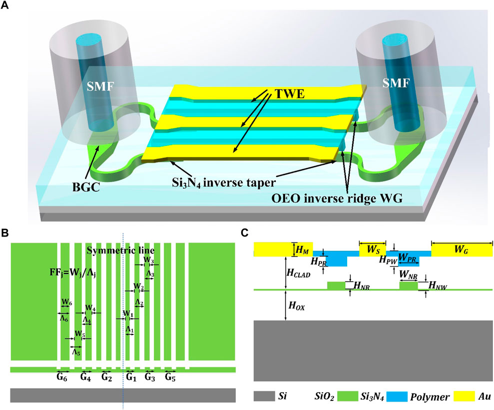
FIGURE 1. (A) The schematic diagram of the structure of the silicon nitride/organic polymer Mach-Zehnder modulator. (B) The schematic view of the silicon nitride bidirectional grating coupler. (C) The cross-sectional view of the hybrid waveguide structure of the vertical mode converter.
The bidirectional grating coupler, as the beam splitter/combiner of the hybrid electro-optic modulator, greatly affects the performance of the whole device [31–33]. The main parameters of the grating coupler include grating pitches, waveguide height, etching depth, duty cycles. When the single mode fiber (SMF) is perfectly aligned with the grating center, the light incident from the optical fiber is coupled and divided into two beams with the same amplitude and phase. Ideally, the BGC should feature low coupling loss, low parasitic reflections and large optical bandwidth. Here, we propose a grating design that fits the design requirements. Figure 1B shows a schematic diagram of the proposed silicon nitride BGC. The grating length is designed as 12 µm. To optimize the device performance, 2D and 3D Finite-Difference Time-Domain (FDTD) simulations were carried out [34]. A series of 2D simulations were carried out for rapid parameter optimization, the 3D simulations were carried out for the performance validation of the finalized design. By optimizing the grating structure parameters, the effective refractive index and coupling strength distribution in the grating plane can be optimized to find the best coupling performance.
For our proposed bidirectional grating coupler, which is both a perfect vertical grating coupler and a 3 dB beam splitter, in-plane optical coupling can be achieved through two access waveguides. Its design process is as follows. Firstly, the effective refractive index of the gratings is estimated by the following equation:
where Neffo and Neffe are the effective indices of the original silicon nitride slab (400 nm-thick) and the etched areas (80 nm-thick),
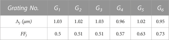
TABLE 1. The parameters of the optimized grating.
Figures 2A, B shows the calculated optical field intensity distribution of in-plane and out-of-plane grating coupling respectively. As can be seen, this device can function well as a perfectly vertical grating coupler. Figure 2C shows the calculated performance of the designed silicon nitride bidirectional grating coupler, where the coupling efficiency (CE), the up-reflection towards fiber (UR) and the waveguide back-reflection (BR) spectra are all presented. The coupling efficiency reaches 70% at a wavelength of 1552 nm, implying that very close mode matching is achieved near the central coupling wavelength between the grating diffraction mode and the fiber mode. In addition, the waveguide back reflection is as low as -20.6 dB, and the minimum value of the upward-reflection to the fiber is 0.02%, corresponding to the return loss of -17 dB. The 1 dB bandwidth of the grating is 27 nm.
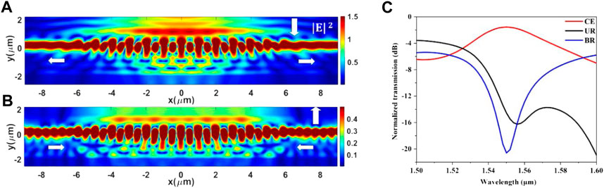
FIGURE 2. (A) Calculated optical field intensity of the bidirectional grating as an input coupler (B) Calculated optical field intensity of the bidirectional grating as an output coupler (C) The performance of vertical bidirectional grating.
Vertical adiabatic mode conversion is an effective way for optical transmission between different waveguide layers in vertical direction [35]. For this device, optical adiabatic transmission is realized by the longitudinal evanescent wave coupling between inversed-taper silicon nitride waveguides and organic polymer waveguides, in which the alignment between the two waveguides is achieved by silicon dioxide cladding etching and organic polymer filling processes. The E-O material utilized in this device is 3:1 HD-BB-OH:YLD124, which has a refractive index of 1.77 near the wavelength of 1550 nm and optical absorption coefficient of 3 × 10⁻⁵ cm−1. As depicted in Figure 1C, the structural parameters of the vertical mode converter (VMC) mainly include silicon dioxide spacer thickness HCLAD and HOX, silicon nitride waveguide height HNW, silicon nitride etching depth HNR, silicon nitride ridge waveguide width WNR, polymer waveguide height HPW, polymer waveguide ridge height HPR, the polymer waveguide width WPR.
The performance of the VMC is simulated using the EigenMode Expansion (EME) solver of Lumerical Mode solutions. To achieve high-efficiency coupling, three key device parameters should be carefully designed and optimized. The three parameters are the thickness of silicon dioxide spacer HCLAD, the VMC length L and the tip width of the silicon nitride inversed taper respectively. After analyzing the influence of these parameters with a series of calculations, an optimized design with 99.2% transmission efficiency is obtained with a device length of 32 µm and tip width of 0.2 µm. Such a design is compact and easy to fabricate, and design values of other parameters are shown in Table 2. Figure 3B shows the calculated optical field distribution of the VMC and the optical mode profiles at different positions along the waveguide direction. Figures 4A, B shows the calculated normalized transmission of the vertical mode converter as a function of taper length and wavelength respectively. In the process, the silicon nitride waveguide and the organic polymer waveguide may cause additional errors due to the incomplete alignment.

TABLE 2. The parameters of mode spot conventer.
FIGURE 3. Longitudinal field distribution of silicon nitride/organic polymer waveguide longitudinal adiabatic mode spot converter (A) the Schematic diagram (B) optical mode field at different positions.
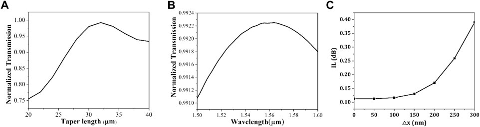
FIGURE 4. The normalized transmission of the vertical mode converter (A) as a function of silicon nitride taper length (B) as a function of wavelength (C) the effect of the center of organic polymer waveguide deviating from the center of silicon nitride waveguide on device insertion loss.
We analyzed the transmission performance of the device when the center of the organic polymer waveguide deviates from the center of the silicon nitride waveguide, and obtained the results which is shown as Figure 4C. As the center of the organic polymer waveguide is shifted to both sides, the transmission performance will be reduced. However, in the range of about 250 nm for each deviation, the device can still maintain the transmission efficiency of more than 98%, and the insertion loss is less than 0.26 dB. Therefore, the device has a strong alignment tolerance.
Figure 5A is a cross section of the polymer optical waveguide, and Figure 5B is a top view of the modulator. The phase shifter is made up by E-O polymer waveguide and coplanar travelling-wave electrodes, where a single-drive push-pull operation scheme is utilized. The E-O material YLD124 combined with HD-BB-OH as the host polymer. The molecular structure of the material is shown in Figure 5B. According to Ref. [36], The electro-optic coefficient r33 can reach the maximum value of 255 pm/V at the wavelength of 1550 nm. Here, the in-device r33 of 150 pm/V is assumed and utilized in simulation. At a certain temperature, by applying a polarization voltage Vpol to the ground electrode, a polarization electric field can be formed in the ridge, and the chromophore dipoles in the electro-optic material are aligned along the polarization field, as indicated by the red arrows in Figures 5A, B. A driving microwave signal Vdrive is applied on the signal electrode, and a strong electric field can be formed across the polymer waveguide. The modulation electric field of the left arm is antiparallel to the polarization direction of the chromophore, and the modulation electric field of the right arm is parallel to the polarization direction of the chromophore, as shown by the purple arrow in Figure 5A, thus realizing push-pull modulation features [37].
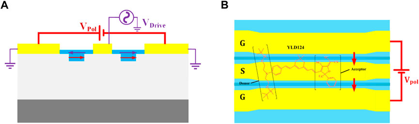
FIGURE 5. The structure diagram of phase shifter (A) the cross section of the optical waveguide (B) the top view of the modulator.
For this E-O polymer modulator, the modulation voltage can be expressed as the following equation [38],
where Vπ is the modulation voltage applied to achieve a π phase shift, L is the phase shifter length, λ is the light wavelength in vacuum, d is the gap between the signal electrode and the ground electrode, and Г represents the E-O overlapping integral factor, which can be expressed as,
where EE(x,y) and EO(x,y) represent the electric field profile induced by the applied voltage and the electric field distribution related to the optical modal profile of the polymer waveguide, A is the cross-sectional area of the polymer waveguide.
From the equation (2) and (3), it can be seen that the key to improve the modulation efficiency is to optimize the structure and relative location of the polymer waveguides and the coplanar travelling wave electrodes, when the E-O material is chosen. Normally, a better optical confinement of the polymer waveguide and a small electrode gap are beneficial to the E-O overlapping integral factor Г. However, decreasing the electrode gap will also lead to a larger overlapping between the electrode and the optical mode and thus a larger optical loss as a result. Therefore, the parameters of the phase shifter and the parameters of the electrodes can be optimized to achieve a compromise between the optical loss and the phase shift efficiency of the phase shifter. The optimization process is carried out using the Ansys Lumerical software package. Figure 6A shows the calculated modulation efficiency and optical loss of the phase shifter as a function of applied voltage and electrode spacing. As can be seen, the modulation efficiency and optical loss are all independent on the applied voltage, which is due to the linear modulation response of the Pockels effect. As a performance tradeoff, the electrode gap is designed as 4 μm, Г is 0.82, where a modulation efficiency of about 1.34 Vcm and optical loss of 9.48 dB/cm are obtained. The relative large optical loss is mainly due to the absorption of the OEO material. However, considering the polymer modulator is millimeter scale, the insertion loss is acceptable. The group refractive index of light wave is 1.81452 in optical simulation. In order to improve the bandwidth of the device, it is necessary to achieve rate matching and impedance matching. In addition, the microwave performance of the electrode is carefully analyzed and optimized for minimized microwave loss and impedance matching. After a series of calculations, all the design parameters are determined as shown in Table 3. Figure 6B shows the microwave loss and characteristic impedance of the travelling wave electrode as a function of microwave frequency. As can be seen, the microwave loss is lower than 14 dB/cm at the frequency of 100 GHz, and the characteristic impedance is around 50 Ω which shows a good impedance matching can be guaranteed. Figures 6C, D show the microwave refractive index and impedance at different signal electrode widths. With the decrease of the width of the signal electrode, the numeric matching between the group index of the microwave and the refractive index of the light wave is improved, which can achieve better rate matching. At the same time, the characteristic impedance is close to 50Ω.
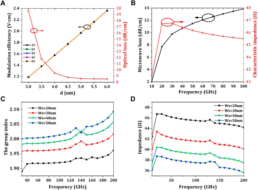
FIGURE 6. The simulation results of phase shifter (A) Modulation efficiency and optical loss as a function of voltage and electrode spacing d (B) The microwave loss and impedance as a function of frequency of the phase shifter (C) The microwave group index under different signal electrode widths as a function of frequency (D) Impedance under different signal electrode widths as a function of frequency.

TABLE 3. The specific structural parameters of the phase shifter.
The proposed silicon nitride/organic polymer hybrid modulator achieves a good balance between high modulation performance, low loss, and thermal stability. For ease of fiber packaging, silicon nitride bidirectional grating couplers are used as optical input/output interface and power splitter/combiner of the MZI modulator. Compared with silicon, silicon nitride exhibits the advantages of similar refractive index with E-O polymer [36], better thermal stability, large fabrication tolerance. To simulate the MZI modulator performance, all the optical components including the bidirectional grating couplers and the vertical mode converters are all modeled and simulated using FDTD or EME method, also S-parameter matrices are extracted for circuit-level simulation. The phase shifters are modeled and simulated with Lumerical Mode solutions and Charge, and then the optimized results and parameters are exported for circuit-level simulation.
Figure 7 shows the simulation link diagram of the modulator. The optical network analyzer (ONA) is adopted to obtain the static transmission spectra of the optical modulator, while a PRBS generator, a symbol mapper and a digital communication analyzer (DCA) are utilized for feeding PAM4 driving signals and eye diagram observation respectively. The length of modulator is chosen to be 3 mm. After setting the static bias conditions of the modulator and the wavelength of the laser, the static spectrum of the hybrid electro-optic modulator is obtained, as shown in Figure 8. Both balanced-arm MZI and unbalanced-arm MZI modulators are designed and simulated respectively, in a push-pull driving scheme. In Figure 8, it is shown that their half-wave voltages are both 2.29 V. Therefore, the modulation efficiency of the push-pull modulator is 0.67 V cm. Figure 9 shows the bandwidth of the modulator at different lengths. It can be seen the device length have a large impact on the bandwidth. In the simulation, the effect of the microwave loss, velocity matching and impedance matching of the device are all considered. Different microwave refractive index and impedance results have been obtained in Figures 6C, D, and the corresponding bandwidth is shown in Figure 9B. With a device length of 3 mm and signal electrode width of 28 μm, a bandwidth of 174 GHz can be obtained.
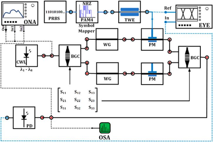
FIGURE 7. The circuit-level simulation diagram of the hybrid silicon nitride/organic polymer modulator.
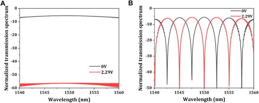
FIGURE 8. The normalized optical transmission spectrum varies with voltage of (A) MZI with balanced arms (B) MZI with unbalanced arms.
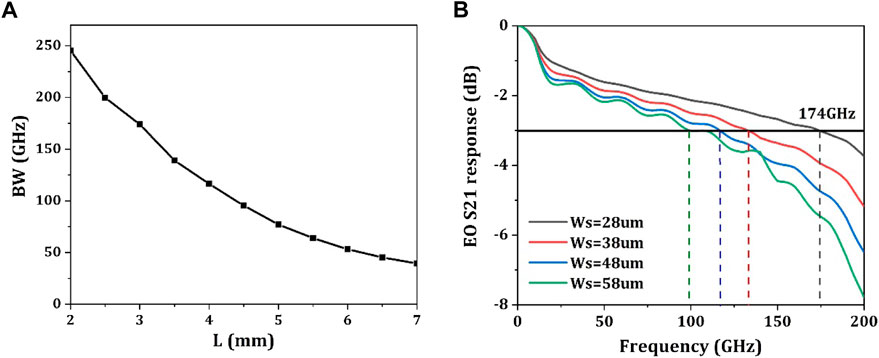
FIGURE 9. (A) Modulator bandwidth at different lengths (B) Modulator bandwidth when L = 3 mm under different signal electrode widths.
Linearity is an important metric when simulating PAM4 eye diagrams. When the linearity is poor, the three eyes of the PAM4 output eye diagram have different heights, and the bit error rate of the eye diagram determines by the smallest eye. RLM is defined in IEEE 802.3bs to evaluate the linearity of the PAM4 eye diagram. VA, VB, VC and VD respectively represent the four level values from top to bottom in PAM4 eye diagram. The calculation formula is as follows:
The FSR of the anisotropic MZI is designed to be 5 nm. At a bias voltage of 1.25 V and a driving peak-to-peak voltage of 1.5 V, the modulator has good linearity. Considering the bandwidth limitation of the measurement setup, a low-pass filter with bandwidth of 65 GHz is utilized in the simulation of eye-diagram tests. In the simulation, the detector has a responsivity is 1A/W, dark current is 0A, and thermal noise is 1e−22 A/Hz^.05. Figure 10 shows the eye diagram of the modulator transmitting a 120 Gbaud PAM4 signal at 1550 nm. When transmitting signal with a balanced-arm MZI modulator, the bit error rate of the eye diagram is 1.58 × 10⁻¹⁵, and the extinction ratio is 4.63 dB, the overall insertion loss of the modulator is 5.74 dB. When transmitting signal with an unbalanced-arm MZI modulator, the bit error rate of the eye diagram is 1.66 × 10⁻¹⁵, and the extinction ratio is 4.38 dB, the overall insertion loss of the modulator is 5.71 dB. The noise and jitter of the eye diagram in Figure 10 are very small, and the PAM4 eye diagram also has good linearity, and its RLM>0.922. In summary, circuit-level simulations show that the modulator functions well both statically and dynamically.
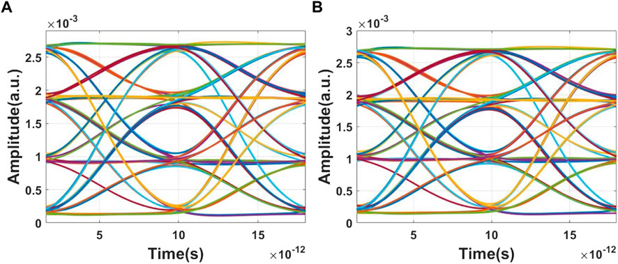
FIGURE 10. Simulated PAM4 eye diagram results. (A) 120Gbaud PAM4 signal of balanced-arm MZI modulator (B) 120Gbaud PAM4 signal of unbalanced-arm MZI modulator.
Table 4 shows the comparison between the state-of-the-art electro-optic modulators based on silicon nitride waveguide platform. As can be seen, our device exhibits the advantage of high bandwidth and low insertion loss. The simulated bandwidth is 174 GHz, which is much higher than that seen in the literature. The insertion loss of our device is 5.74 dB, which include two grating coupling loss of 3.08 dB. Compared with other polymer/silicon nitride hybrid designs [41, 28, 43], our design shows the advantages of high bandwidth, high modulation efficiency and low insertion loss. The length of the active region of the structure is only 3 mm. Although the micro-ring modulator is smaller in size, it is more sensitive to the manufacturing tolerance and temperature change. In addition to the deposition of organic polymers on silicon nitride, there are also the deposition of PZT or ZnO structures. But the annealing temperature required for PZT [25, 42] deposition is about 620°, and such a high temperature can lead to compatibility problems with the metal process. When ZnO [26] material is deposited by atomic layer technology, the electro-optical coefficient of the electro-optical material is small, and the phase shift efficiency of the device is poor. In addition, the bandwidth of the device is limited by the photon lifetime of the microring resonator and the RC time constant, and the bandwidth is very small, less than GHz. Although organic polymer-based modulators show good performance, organic polymer materials are not compatible with the current CMOS process, so the integration process of organic polymer materials with silicon nitride needs to be carefully designed and discussed.
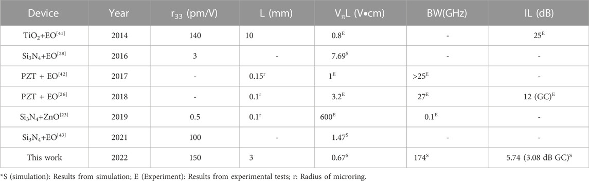
TABLE 4. The performance comparison of modulators with different structures.
The process flow of the hybrid modulator is depicted in Figure 11. The fabrication starts from a silicon nitride on insulator platform. With Deep Ultraviolet Lithography (DUV) lithography and Inductively Coupled Plasma (ICP) etching, the silicon nitride waveguides are patterned. Then silicon dioxide cladding is deposited by plasma enhanced chemical vapor deposition (PECVD). Then chemical mechanical polishing is utilized for planarization and thinning of the overlayer. Next, metal electrodes are deposited and patterned by electron beam evaporation, DUV lithography and dry etching. After patterning of the metal electrodes, silicon dioxide cladding trenches need to be formed for the polymer waveguides. The above processes are all standard semiconductor technologies and CMOS compatible. As for the last step of device fabrication, polymer waveguide integration is the key process. There are two feasible methods, namely, the traditional spin coating process and the microfluidic filling process. For spin coating process [39], the film quality is largely dependent on the solvent and rotational speed. When choosing a solvent, the solubility of the material and the evaporation rate of the solvent are the two main factors. When the evaporation rate of the solution is high, the intermediate operation steps must be fast to avoid the solution becoming viscous and unable to obtain a high-quality film, and the spin coating time is usually kept below 3 s. In addition, the agglomeration of chromophores during the spin coating process will also make the film non-uniform, resulting in increased waveguide loss, and sometimes wrinkles will appear on the surface of the polymer film, which will destroy the quality of the film waveguide. Theoretically, the film thickness is a function of viscosity, solution density, spin time and spin speed, which can be measured by an ellipsometer. This method is simple in process, but wastes materials and may affect the performance of surface devices.
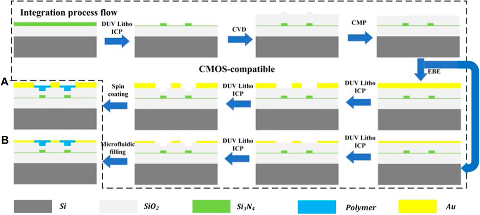
FIGURE 11. Two integrated process solutions for silicon nitride/organic polymer hybrid waveguide modulators. (A) The traditional spin coating process (B) The microfluidic filling process.
The second method is the microfluidic trench filling process [40], which is relatively new in the fabrication of polymer waveguides. Figure 12 shows the fabrication flow of polymer waveguides based on the microfluidic trench filling process. As can be seen, the process is divided into four steps. Firstly, a closed microfluidic channel can be formed by the metal electrode gap and the silicon dioxide trench. Then a microfluidic mold is produced, using glass as the substrate and spin-coating photoresist on the substrate as a sacrificial layer. After the photoresist is cured, two holes need to be etched through to form a liquid input and output. Through alignment and bonding process, the microfluidic mold and the chip surface are connected to realize a closed micro-channel cavity. Then the polymer waveguide can be formed by a microfluidic filling process. When the filling process is completed, the polymer waveguides are cured at high temperature. At the last step, the photoresist sacrificial layer is removed and the glass mold is peeled off. In this method, the polymer waveguide can be automatically formed and positioned, but it requires careful design of the metal electrode thickness, which will lead to a tradeoff of the electrode performance.
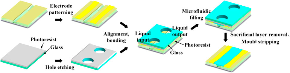
FIGURE 12. The schematic diagram of the fabrication process of organic polymer waveguides based on microfluidic injection technology.
In conclusion, we propose a hybrid silicon nitride/polymer optical modulator based on longitudinal evanescent wave coupling. Silicon nitride bidirectional grating coupler is designed to realize perfectly vertical coupling and beam splitting/combining, and Mach-Zehnder interferometer can be formed with the back-to-back configuration of this grating coupler. The simulation results show that the maximum coupling efficiency reach 70%, which is very suitable for low-loss integration. To achieve adiabatic transfer between silicon nitride waveguide and polymer waveguide, inverse taper based vertical mode converter is designed. Simulation shows a transmission of 99.2% can be obtained with a taper length of only 32 µm. By optimize the waveguide structure and electrode design, performance tradeoff between the optical loss and modulation efficiency can be achieved for the phase shifter. After simulation, the insertion loss of the modulator is 5.74 dB, including two grating coupler losses of about 3.08 dB. The eye diagram test results show that the modulator can support up to 120 Gbaud PAM4 signal transmission, the bit error rate meets the optical communication transmission standard, and the data transmission rate still has room for improvement.
The original contributions presented in the study are included in the article/Supplementary Material, further inquiries can be directed to the corresponding author.
Methodology and writing- original draft, BH; Writing and formal analysis, ZZ; Data analysis and interpretation, ML; Survey and collection of data, KZ; Review and editing, TL; Investigation, HJ; Investigation, QW; Investigation, JX.
This research was funded by the National Key R&D Program of China (Grant No. 2018 YFA0209000), the Natural Science Foundation of China (Grant Nos. 61675191, 61974099, 61634006, 61675154, 61704009), the Youth Innovation Promotion Association of Chinese Academy of Sciences under Grant No. 2018146, Tianjin Research Program of Application Foundation and Advanced Technology of China (20JCQNJC00180).
The authors would like to thank Zan Zhang from Chang’an University for fruitful discussions.
The authors declare that the research was conducted in the absence of any commercial or financial relationships that could be construed as a potential conflict of interest.
All claims expressed in this article are solely those of the authors and do not necessarily represent those of their affiliated organizations, or those of the publisher, the editors and the reviewers. Any product that may be evaluated in this article, or claim that may be made by its manufacturer, is not guaranteed or endorsed by the publisher.
The Supplementary Material for this article can be found online at: https://www.frontiersin.org/articles/10.3389/fphy.2022.1079167/full#supplementary-material
1. Liu A, Jones R, Liao L, Samara-Rubio D, Rubin D, Cohen O, et al. A high-speed silicon optical modulator based on a metal–oxide–semiconductor capacitor. Nature (2004) 427:615–8. doi:10.1038/nature02310
2. Reed G, Mashanovich G, Gardes F, Thomson D. Silicon optical modulators. Nat Photon (2010) 4:518–26. doi:10.1038/nphoton.2010.179
3. Xiao X, Xu H, Li X, Li Z, Chu T, Yu Y, et al. High-speed, low-loss silicon Mach–Zehnder modulators with doping optimization. Opt Express (2013) 21:4116–25. doi:10.1364/OE.21.004116
4. Reed G, Mashanovich G, Gardes F, Nedeljkovic M, Hu Y, Thomson D, et al. Recent breakthroughs in carrier-depletion based silicon optical modulators. Nanophotonics (2014) 3:229–45. doi:10.1515/nanoph-2013-0016
5. Li K, Liu S, Thomson D, Zhang W, Yan X, Meng F, et al. Electronic–photonic convergence for silicon photonics transmitters beyond 100 Gbps on–off keying. Optica (2020) 7:1514–6. doi:10.1364/OPTICA.411122
6. Ogawa K, Goi K, Tan Y, Liow T, Tu X, Fang Q, et al. Silicon Mach-Zehnder modulator of extinction ratio beyond 10 dB at 10.0-12.5 Gbps. Opt Express (2011) 19:B26–B31. doi:10.1364/OE.19.000B26
7. Dong P, Chen L, Chen Y. High-speed low-voltage single-drive push-pull silicon Mach-Zehnder modulators. Opt Express (2012) 20:6163–9. doi:10.1364/OE.20.006163
8. Yang Y, Fang Q, Yu M, Tu X, Rusli R, Lo G. High-efficiency Si optical modulator using Cu travelling-wave electrode. Opt Express (2014) 22:29978–85. doi:10.1364/OE.22.029978
9. Marris-Morini D, Virot L, Baudot C, Fédéli J, Rasigade G, Perez-Galacho D, et al. A 40 Gbit/s optical link on a 300-mm silicon platform. Opt Express (2014) 22:6674–9. doi:10.1364/OE.22.006674
10. Li M, Wang L, Xiang L, Xiao X, Yu S Silicon intensity Mach–Zehnder modulator for single lane 100 Gb/s applications. Photon Res (2018) 6:109–16. doi:10.1364/prj.6.000109
11. Miura H, Qiu F, Spring A, Kashino T, Kikuchi T, Ma O, et al. High thermal stability 40 GHz electro-optic polymer modulators. Opt Express (2017) 25:28643–9. doi:10.1364/OE.25.028643
12. Melikyan A, Koehnle K, Lauermann M, Palmer R, Koeber S, Muehlbrandt S, et al. Plasmonic-organic hybrid (POH) modulators for OOK and BPSK signaling at 40 Gbit/s. Opt Express (2015) 23:9938–46. doi:10.1364/OE.23.009938
13. Kieninger C, Kutuvantavida Y, Elder D, Wolf S, Zwickel H, Blaicher M, et al. Ultra-high electro-optic activity demonstrated in a silicon-organic hybrid modulator. Optica (2018) 5:739–48. doi:10.1364/OPTICA.5.000739
14. Elder D, Haffner C, Heni W, Fedoryshyn Y, Garrett K, Johnson L, et al. Effect of rigid bridge-protection units, quadrupolar interactions, and blending in organic electro-optic chromophores. Chem Mater (2017) 29:6457–71. doi:10.1021/acs.chemmater.7b02020
15. Dalton L, Sullivan P, Bale D. Electric field poled organic electro-optic materials: State of the art and future prospects. Chem Rev (2010) 110:25–55. doi:10.1021/cr9000429
16. Alloatti L, Palmer R, Diebold S, Pahl K, Chen B, Dinu R, et al. 100 GHz silicon–organic hybrid modulator. Light Sci Appl (2014) 3:173. doi:10.1038/lsa.2014.54
17. Qiu F, Spring A, Hong J, Yokoyama S. Plate-slot polymer waveguide modulator on silicon-on-insulator. Opt Express (2018) 26:11213–21. doi:10.1364/OE.26.011213
18. Burla M, Hoessbacher C, Heni W, Haffner C, Fedoryshyn Y, Werner D, et al. 500 GHz plasmonic Mach-Zehnder modulator enabling sub-THz microwave Photonics. APL Photon (2019) 4:056106. doi:10.1063/1.5086868
19. Heni W, Haffner C, Baeuerle B, Fedoryshyn Y, Josten A, Hillerkuss D, et al. 108 Gbit/s plasmonic mach–zehnder modulator with > 70-GHz electrical bandwidth. J Lightwave Technol (2016) 34:393–400. doi:10.1109/JLT.2015.2487560
20. Koch U, Uhl C, Hettrich H, Fedoryshyn Y, Hoessbacher C, Heni W, et al. A monolithic bipolar CMOS electronic–plasmonic high-speed transmitter. Nat Electron (2020) 3:338–45. doi:10.1038/s41928-020-0417-9
21. Blumenthal D, Heideman R, Geuzebroek D, Leinse A, Roeloffzen C. Silicon nitride in silicon photonics. Proc IEEE (2018) 106:2209–31. doi:10.1109/JPROC.2018.2861576
22. Wang J, Zhang X, Chen Y, Geng Y, Du Y, Li X. Design of a graphene-based silicon nitride multimode waveguide-integrated electro-optic modulator. Opt Commun (2021) 481:126531. doi:10.1016/j.optcom.2020.126531
23. Hermans A, Daele M, Dendooven J, Clemmen S, Detavernier C, Baets R. Integrated silicon nitride electro-optic modulators with atomic layer deposited overlays. Opt Lett (2019) 44:1112–5. doi:10.1364/OL.44.001112
24. Phare C, Daniel L, Cardenas Y, Lipson M. Graphene electro-optic modulator with 30 GHz bandwidth. Nat Photon (2015) 9:511–4. doi:10.1038/nphoton.2015.122
25. Alexander K, George J, Verbist J, Neyts K, Kuyken B, Thourhout D, et al. Nanophotonic Pockels modulators on a silicon nitride platform. Nat Commun (2018) 9:3444. doi:10.1038/s41467-018-05846-6
26. Hermans A, Daele M, Dendooven J, Clemmen S, Detavernier C, Baets R. Integrated silicon nitride electro-optic modulators with atomic layer deposited overlays. Opt. Lett. (2019) 44:1112–1115. doi:10.1364/OL.44.001112
27. Ahmed A, Nelan S, Shi S, Yao P, Mercante A, Prather D. Subvolt electro-optical modulator on thin-film lithium niobate and silicon nitride hybrid platform. Opt Lett (2020) 45:1112–5. doi:10.1364/OL.381892
28. Baudzus L, Krummrich P. Low loss electro-optic polymer based fast adaptive phase shifters realized in silicon nitride and oxynitride waveguide technology. Photonics (2016) 3:49. doi:10.3390/photonics3030049
29. Rutirawut T, Talataisong W, Gardes F. Designs of silicon nitride slot waveguide modulators with electro-optic polymer and the effect of induced charges in Si-substrate on their performance. IEEE Photon J (2021) 13:1–15. doi:10.1109/JPHOT.2021.3059276
30. Zan Z, Bei H, Zan Z, Chuan C, Hong C. Bidirectional grating coupler based optical modulator for low-loss Integration and low-cost fiber packaging. Opt Express (2013) 21:14202–14. doi:10.1364/OE.21.014202
31. Chmielak B, Suckow S, Parra J, Duarte V, Mengual T, Piqueras M, et al. High-efficiency grating coupler for an ultralow-loss Si3N4-based platform. Opt Lett (2022) 47:2498–501. doi:10.1364/OL.455078
32. Ghannam I, Merget F, Witzens J. Silicon nitride C-band grating couplers with reduced waveguide back-reflection. Opt Interconnects (2022) XXII:120070N. Proc. SPIE 12007. doi:10.1117/12.2607729
33. Hong J, Spring A, Qiu F, Yokoyama S. A high efficiency silicon nitride waveguide grating coupler with a multilayer bottom reflector. Sci Rep (2019) 9:12988. doi:10.1038/s41598-019-49324-5
34. Kane Y. Numerical solution of initial boundary value problems involving maxwell's equations in isotropic media. IEEE Trans Antennas Propag (1966) 14:302–7. doi:10.1109/TAP.1966.1138693
35. He M, Xu M, Ren Y, Jian J, Ruan Z, Xu Y, et al. High-performance hybrid silicon and lithium niobate Mach–Zehnder modulators for 100 Gbit s−1 and beyond. Nat Photon (2019) 13:359–64. doi:10.1038/s41566-019-0378-6
36. Elder D, Haffner C, Heni W, Fedoryshyn Y, Garrett K, Johnson L. Effect of Rigid Bridge Protection Units, Quadrupolar Interactions, and Blending in Organic Electro-Optic Chromophores. Chemistry of Materials (2017): 6457–6471. doi:10.1021/acs.chemmater.7b02020
37. Heni W, Haffner C, Elder D, Tillack A, Fedoryshyn Y, Cottier R, et al. Nonlinearities of organic electro-optic materials in nanoscale slots and implications for the optimum modulator design. Opt Express (2017) 25:2627–53. doi:10.1364/OE.25.002627
38. Kamada S, Ueda R, Yamada C, Tanaka K, Yamada T, Otomo A. Superiorly low half-wave voltage electro-optic polymer modulator for visible photonics. Opt Express (2022) 30:19771–80. doi:10.1364/OE.456271
39. Hikita M, Yoshimura R, Usui M, Tomaru S, Imamura S. Polymeric optical waveguides for optical interconnections. Thin Solid Films (1998) 331:303–8. doi:10.1016/S0040-6090(98)00935-3
40. Lien V, Berdichevsky V, Lo Y. A prealigned process of integrating optical waveguides with microfluidic devices. IEEE Photon Technol Lett (2004) 16:1525–7. doi:10.1109/LPT.2004.826774
41. Qiu F, Spring A, Maeda D, Ozawa M, Odoi K, Otomo A, et al. A hybrid electro-optic polymer and TiO2 double-slot waveguide modulator. Sci Rep (2015) 5:8561. doi:10.1038/srep08561
42. Alexander K, George JP, Kuyken B, Beeckman J, Van Thourhout D. Broadband electro-optic modulation using low-loss PZT-on-silicon nitride integrated waveguides. CLEO: Appl Tech (2017) 7:JTh5C. doi:10.1364/CLEO_AT.2017.JTh5C.7
Keywords: perfectly vertical grating coupler, vertical mode-spot converters, hybrid waveguide modulator, silicon nitride waveguide, organic polymer waveguide
Citation: Huang B, Zhang Z, Li M, Zhang K, Liu T, Jiang H, Wang Q and Xing J (2022) Simulation of hybrid silicon nitride/polymer Mach-Zehnder optical modulator beyond 170 GHz. Front. Phys. 10:1079167. doi: 10.3389/fphy.2022.1079167
Received: 25 October 2022; Accepted: 06 December 2022;
Published: 15 December 2022.
Edited by:
Lorenzo Pavesi, University of Trento, ItalyReviewed by:
Sheng Xie, Tianjin University, ChinaCopyright © 2022 Huang, Zhang, Li, Zhang, Liu, Jiang, Wang and Xing. This is an open-access article distributed under the terms of the Creative Commons Attribution License (CC BY). The use, distribution or reproduction in other forums is permitted, provided the original author(s) and the copyright owner(s) are credited and that the original publication in this journal is cited, in accordance with accepted academic practice. No use, distribution or reproduction is permitted which does not comply with these terms.
*Correspondence: Beiju Huang, YmpodWFuZ0BzZW1pLmFjLmNu
Disclaimer: All claims expressed in this article are solely those of the authors and do not necessarily represent those of their affiliated organizations, or those of the publisher, the editors and the reviewers. Any product that may be evaluated in this article or claim that may be made by its manufacturer is not guaranteed or endorsed by the publisher.
Research integrity at Frontiers
Learn more about the work of our research integrity team to safeguard the quality of each article we publish.