
94% of researchers rate our articles as excellent or good
Learn more about the work of our research integrity team to safeguard the quality of each article we publish.
Find out more
ORIGINAL RESEARCH article
Front. Phys., 24 November 2022
Sec. Optics and Photonics
Volume 10 - 2022 | https://doi.org/10.3389/fphy.2022.1069099
This article is part of the Research TopicSilicon-Based Optoelectronics and Microelectronics Integration TechnologyView all 7 articles
Inspired by the mechanism of visual attentional selection, a wireless optical communication (WOC) Integrated receiver consisting of a vertical double junction photodetector (VDJ-PD) and an attentional selection circuit (ASC) is presented. The whole receiver is fabricated in standard CMOS technology. The VDJ-PD can realize optical signal detection and wavelength identification. The attentional selection circuit activates the competition among the two PN junctions in VDJ-PD to select the signal with significant feature in real-time while discarding non-significant signals. A higher-order signal modulation scheme is applied by the proposed receiver to obtain a high transfer rate, and all data are decoded using color features. The optical testing results show that parallel and real-time communication of the red and blue light can be achieved, and the rise time is 4.47 μs. To measure the anti-interference performance of the receiver, a water tank is used to simulate a harsh communication environment. Results indicate that the real-time and reliable communication requirements in a harsh channel condition are satisfied. When the percentage ratio between the intensity of stray light relative to the light with maximum intensity is 84%, an accurate information decoding can still be achieved. Moreover, the whole processing procedure does not require the participation of ADC, CPU and memory, consequently avoiding the von Neumann bottleneck.
Wireless optical communication (WOC) is a form of optical communication in which unguided visible, infrared (IR), or ultraviolet (UV) light is used to carry signals and is considered a viable solution for achieving high-speed and large-capacity communication links [1–4]. It plays an irreplaceable role and has broad application prospects in confidentiality [5]; [6], cellular connectivity support, and underwater communication [7]; [8]; [9]. However, owing to the fact that light travels in a straight line-light path [10], the alignment and time-varying fading channels bring a considerable burden to the system. Especially, the higher-order signal modulation schemes based on amplitude modulation, such as PAM4 [11], may encounter significant challenges in the time-varying channel fading of underwater channels [12]; [13]. To separate signals of interest from the entire signals, the optical communication systems based on amplitude modulation need to perform digital signal processing, such as analog-to-digital conversion (ADC), quantization, and comparison [14]. With the increase in the communication rate and the modulation order [15], the delay of the system and the power required for data processing rise exponentially. With the boom of deep learning, data processing models based on artificial neural networks are applied to the WOC systems [16]; [17]. However, deep neural network models typically require a large amount of training data [18]; [19], and the requirement for real-time is challenging to meet simultaneously [20]. Besides, most algorithms are only valid for a certain channel environment, so it is difficult to cope with complex and variable communication environments. Therefore, it is of great significance for promoting the development of the optical communication field to design a channel-fading-resistant WOC receiver with real-time signal processing, high transfer rate, low power consumption, and high anti-interfering ability.
Color is one of the most potent and apparent elements of visual attributes of all primates, including humans [21]; [22]. The color recognition process of the brain is shown in Figure 1, the photoreceptor cells located in the retina transform visible light into nerve impulses [23]. The attention-based neural networks enhance selectivity and contrast by weakening the response of nerve impulses near significant color features to complete color recognition [24]. The fact that the brain can deal successfully and meaningfully with the information for human beings to sense changes in their surroundings owes much to the mechanism of attentional selection [25]. It allows the brain to select pertinent information relevant to the current behavior dynamically while suppressing irrelevant distractors [26]. The human visual system can enhance the selectivity and contrast of the signals through attention selection, that is, it can achieve effective feature selection through the relative strength of signals.
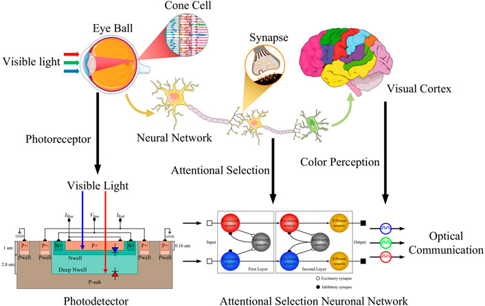
FIGURE 1. The functional diagram of the proposed receiver inspired by visual attentional selection. The optical receiver proposed in this paper can realize the synchronous reception of the red and blue light and the adaptive selection of real-time salient features, and has the autonomy and selectivity similar to that of human beings [29].
Inspired by the visual attentional selection, the proposed receiver designed in this paper explores a biologically plausible framework as shown in Figure 1. The proposed receiver can select the significant feature of the visible light under the interference of stray light, and all of the data are processed and analyzed at a low power level without the participation of ADC, CPU and memory, overcoming the von Neumann bottleneck [27]; [28]. The proposed receiver can be devided into two main functional blocks. The first block is the vertical double junction photodetector (VDJ-PD) distinguishing photons of different wavelengths and converting them into electronic signals. The second block is the feature-selective module, where the attentional selection circuit (ASC) emulates the visual attentional selection and shifts its attention to the most behaviorally-relevant information in real-time.
For semiconductors, silicon is an indirect bandgap semiconductor [30]. When the light with a certain wavelength is incident into the silicon, it absorbs energy and leads to the generation of electron–hole pairs. The number of photons generated in an illuminated semiconductor per second per unit area or photon flux φ(x, λ) by incident light of intensity I (x, λ) is given by:
where E is the photon energy, h is Planck’s constant. And the number of photons generated per second per unit volume is known as Optical Generation Rate, G (x, λ), is given by:
where α(λ) is the optical absorption coefficient, I0 is the intensity factors.
According to Lambert-Beer’s law [31], the optical absorption coefficient determines the penetration depth of light in silicon, which is strongly wavelength dependent [32]. Based on the differences in the penetration depth for various wavelengths of light, a VDJ-PD with different junction depth is designed for the WOC receiver. The VDJ-PD is implemented in the TSMC 0.18 μm standard CMOS technology, and it does not require additional wavelength-selective filters [33] allowing the proposed cell to be further miniaturized and integrated. The cross section of the proposed VDJ-PD is shown in Figure 2A. The shallow Pimp/Nwell junction and Psub/Deep Nwell junction are constituted by stacking vertically Pimp, Nwell, Deep Nwell, and Psub layers in turn. The junction depth corresponds to the silicon’s penetration depth of blue and red light [34]. The photocurrent IBlue and IRed related to the wavelength of the incident light can be obtained by collecting the photogenerated carriers at different depths with the diodes applied with a negative voltage bias. Meanwhile, a guard ring is placed around the VDJ-PD to reduce the interferences caused by the stray current of the subsequent circuits or substrate.
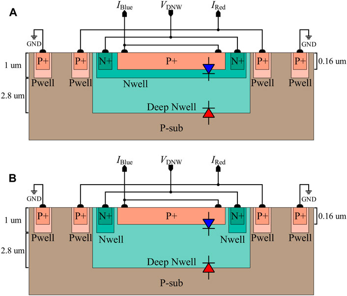
FIGURE 2. The cross section of the VDJ-PD. (A) Pimp/Nwell/Deep Nwell/Psub; (B) Pimp/Deep Nwell/Psub.
Silvaco technology computer-aided design (TCAD) simulations are used to verify the characteristics of the proposed VDJ-PD, and its quantum efficiency is shown in Figure 3. The figure shows that the PD is sensitive to red and blue light, whose center wavelengths are 650 nm and 450 nm. In addition, the transit time of carriers is accelerated with the participation of Nwell layer, so the quantum efficiency of the deep Psub/Deep Nwell junction in the proposed VDJ-PD increases by 26% compared with the Pimp/Deep Nwell/Psub VDJ-PD shown in Figure 2B.
In all primates, attention is a critical factor in the regulation of behavior and neurocognitive functioning. The attentional selection works throughout the brain and participates in almost every stage from sensory processing to decision-making and cognition. The silicon-based MOS transistors operating in the sub-threshold state have the work function to model biological processes, so they can achieve a physical process to cell membrane current regulation of biological neurons with low power consumption [35]; [36]. Based on the characteristic, a double-branch ASC for color feature selection is proposed, and its structure is shown in Figure 4. The circuit is essentially a two-layer attentional selection neural network, and it can perform data processing at the data position without the participation of other digital signal processing modules and memory, consequently avoiding the von Neumann bottleneck.
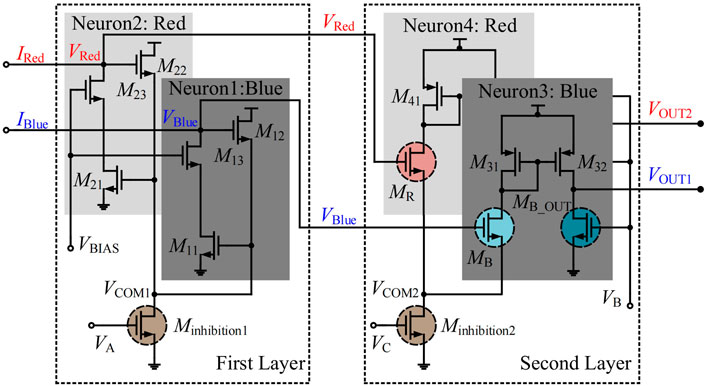
FIGURE 4. The double-branch attentional selection circuit. A higher-order signal modulation scheme can be achieved with the participation of the first layer and the second layer, and the second layer of the attentional selection network can further analysis the signals.
The current of the VDJ-PD, IBlue and IRed, serves as inputs to the first layer of the attentional selection network. In the first layer, VBlue and VRed, the evaluation node, are used as inputs to the second layer network. For different input currents, such as IRed = I and IBlue = I + ΔI, the node voltage VBlue increases, and since the Source voltage of the transistor follows the change of the Gate voltage, the common node voltage Vcom1 also increases until IBlue equals to the Drain current of the transistor M11. With the increase of Vcom1, IRed mismatches the Drain current of transistor M21, so the voltage of VRed decreases and gradually approaches 0 V to maintain the balance. Finally, only the evaluation node of the branch corresponding to the attentional focus is not 0 V. To improve the accuracy and resolution of the circuit, a cascode topology is selected for transistors M11, M13, M21, and M23 to increase the circuit’s gain, and M11 and M21 have as high as possible aspect ratio. Following the processing of the first layer network, VBlue and VRed correlate positively with the photoreceptor’s current. In the second layer of the proposed network, the input transistors MB and MR are operated in the subthreshold region. And the Drain currents increase exponentially with the increasing VGS, thus making the circuit extremely sensitive to the variation of inputs. The tail current transistor Minhibition2 mediates global inhibition through the common node Vcom2. For the assumed current input of the first layer neural network (IRed < IBlue), the voltage of the evaluation node VBlue is stronger than VRed, and the branch corresponding to the MB gets most of the current from Minhibition2, making the voltage of the common node Vcom2 increase. The Source voltage of the input transistors follows the Gate voltage change, so Vcom2 also increases. Since all input transistors share a common Source, the responses of another branch are suppressed until it is turned off. Finally, only the branch with the maximum input can remain active, and its output voltage is equal to the circuit’s supply voltage.
The DC post-simulation results of the ASC are shown in Figure 5. Where IBlue = 10μA, and IRed gradually increases from 8 μA to 12 μA. It can be seen that the output voltage variation tendency of the first layer is the same as that of the second layer. When the difference in the input currents is large, the circuit only pays attention to the branch with the maximum input. As IBlue approaches IRed, the ASC adjusts its attention according to the inputs in real-time, and its voltage output is positively correlated with current inputs. The current resolution of ASC is defined as the minimum current difference that the circuit can recognize. It can be concluded that the current resolution is about 0.14 μA from the post-simulation results. The circuit can switch from the adjustment state to the steady state with an absolute winner once the input difference is outside the resolution. Moreover, the second layer of the attentional selection network can further optimize the resolution and output waveform of the first layer network. Compared with the first layer, the resolution of the circuit is improved at least an order of magnitude. The circuit can reduce the power consumption by closing the branch of the loser, and the transient response time of the circuit to the current change is 2.13 ns, which can meet the real-time requirement of wireless optical communication. The performance comparison between the proposed ASC and other MAX selection circuits is shown in Table 1. It can be seen that the ASC designed in this paper has apparent advantages in resolution and transient response time, which makes it possible to recognize red and blue light with high efficiency, real-time and low power consumption.
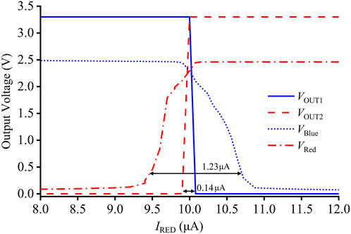
FIGURE 5. DC response of the ASC. It can be seen that ASC can achieve attentional concentration and distraction, and compared with the first layer, the resolution of the circuit is improved at least an order of magnitude. For the first layer, there can be double attentional focuses when the inputs are close.
Fabricated in the TSMC 0.18 μm standard CMOS technology, the micrograph is shown in Figure 6A. The proposed WOC receiver, including pads, occupies an area of 1500 μm × 700 μm, whereas the core area of the ASC chip is only 0.0396 mm2 (300 μm × 132 μm), and the VDJ-PD with guard ring is 600 μm in diameter. All the pads of the chip were marked in the figure, and the chip was mounted on a test Printed Circuit Board (PCB) using bonding wires, as shown in Figure 6B.
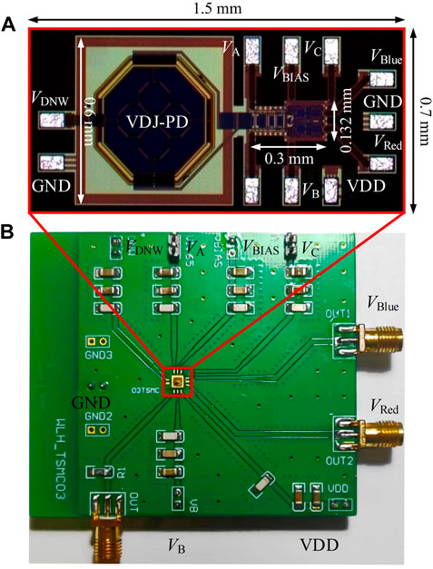
FIGURE 6. The channel-fading-resistant WOC receiver. (A) The micrograph of the receiver; (B) The test PCB of the receiver.
The schematic of the testing setup to measure the optical characteristics is illustrated in Figure 7A. The blue laser (PL, 450B) and red laser (HL, 6501 MG) are used as the experimental light source, whose central wavelengths are 450 nm and 658 nm. The experimental setup is shown in Figure 7B. To prove that the proposed WOC receiver has an excellent anti-interference capacity, a water tank is used to simulate a harsh communication channel, such as signal attenuation and interference. The stabilized voltage supply is used to provide DC voltage for the ASC. The final results are displayed on the Digital oscilloscope (DS6104, Rigol).
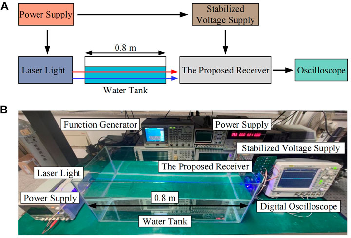
FIGURE 7. The testing setup of the proposed receiver cell. (A) The schematic of testing setup; (B) The experimental setup of the proposed cell. The underwater channel, the most challenging channels for data communications, is selected to evaluate the channel-fading-resistant ability of the optical receiver, and the water tank is used to simulate the harsh communication channel.
To confirm the characteristic of the proposed WOC receiver, steady-state optical measurements were carried out. The VDJ-PD is subjected to random light illumination (blue, red) at the test point, and the change of incident light and the corresponding output results are shown in Figure 8. The light intensity of red and blue light at the laser’s surface is about 120 mW/cm2 measured by optical power meter (PM100D, Thorlabs). Due to the optical attenuation caused by the water tank, the light intensity of blue and red light irradiated on the photoreceptor is about 80 mW/cm2 and 60 mW/cm2, respectively. Note that the cell is able to accurately recognize the blue and red light and the corresponding branch output 3.3V. Moreover, the corresponding values of the output voltage (VBlue, VRed) can be transformed into the binary format as the color labels, which can interpret and define the color of visible light received by the PD. From the experimental results, the WOC receiver can suppress the redundant signals and interference caused by stray light, thus reducing the negative impact on wireless optical communication caused by the spectral overlap of the VDJ-PD and the difficulties of subsequent signal processing.
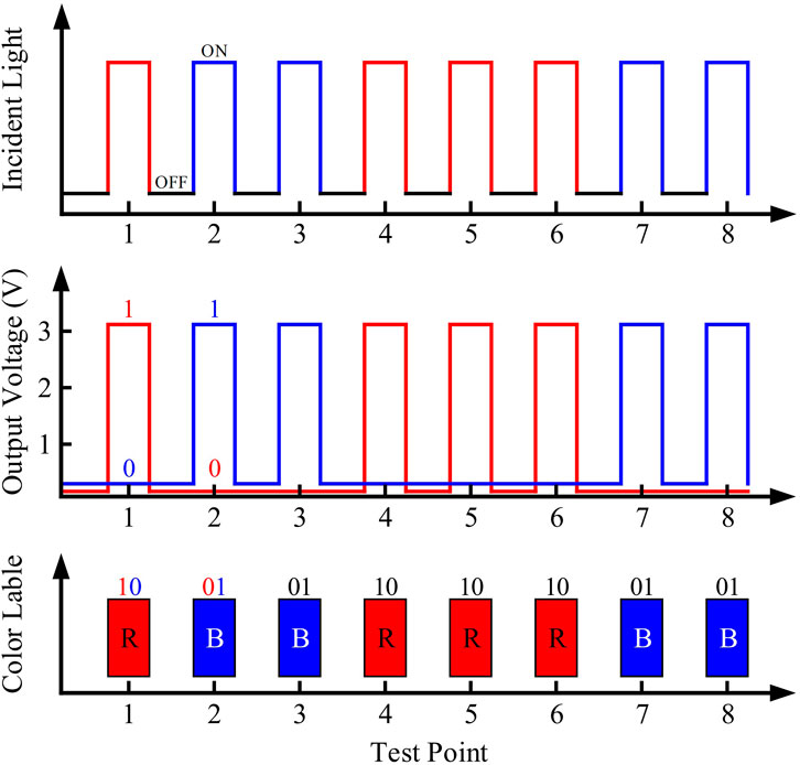
FIGURE 8. The steady-state optical measurements of the proposed receiver. The receiver is able to accurately recognize the blue and red light, and the corresponding outputs can be used as the color label of the visible light.
Dynamic recognition measurements were carried out to evaluate the WOC receiver’s dynamic optical characteristics and attentional sensitivity. During the dynamic test, a square wave signal as the driving voltage of the laser light is modulated with the digital function generator (AFG 3022, Tektronix) to obtain the periodical visible light. When the driving voltage is high, a sufficiently strong light at 70 mW/cm2 is illuminated on the surface of the VDJ-PD, while when the driving voltage is low, the VDJ-PD does not respond to the incident light. The driving voltage of the laser and the cell’s output results are shown in Figure 9A and Figure 9B. Note that the proposed WOC receiver can achieve the color feature selection and focus it’s attention on the branch with the most prominent visible light feature in real-time, completing the optical communication of visible light. The achievable rise time is 4.47 μs. However, compared with blue light at 10 kHz, there is a significant delay in the recognition results of the red light with the same frequency. This may be due to the fact that the red light is absorbed in the deep junction Deep Nwell/Psub of the VDJ-PD, which is vulnerable to bandwidth limitations by the photoresponse time of the PD, mainly determined by the slow carrier dynamics in the substrate [40]; [41]. Nevertheless, the proposed WOC receiver designed in this paper is compatible with the standard CMOS fabrication process. The monolithic integration of PD and ASC is of great importance for the WOC systems with low power consumption and complexity, real-time and miniaturization.
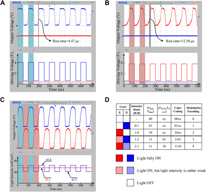
FIGURE 9. Dynamic recognition measurements of the color recognition unit. (A) Blue light: 10 kHz; (B) Red light: 10 kHz; (C) The red and blue light measurements; (D) The color coding of the cell. It can be seen that the receiver can shift its attention according to the change of green light. For further confirmation, it can recognize the on-off lights in different periods, and the results show the periodic changes of color connected with the incident light. When (VBlue, VRed)=(1,1), the optical receiver takes color as the data discrimination basis to achieve a higher-order signal modulation scheme.
To further analyze the anti-interference capacity of the WOC receiver, the red laser is driven by a DC voltage source, and the blue laser is driven by a square-wave voltage signal provided by the digital function generator. When the driving voltage is high, the intensity of blue light is much higher than that of red light. Conversely, when the driving voltage is low, the intensity of red light is much higher than that of blue light. The blue and red light alternately became the single-color light with the maximum intensity. In addition, the intensity of the red light increases gradually with increasing its driving voltage. Figure 9C illustrates the final intensity of the red and blue light and the corresponding output results. Note that the receiver can achieve accurate blue light communication with the interference of red light, and the maximum intensity ratio of the blue light to the red light is 84%. Experimental results demonstrate that the proposed receiver has a strong anti-interference ability, and the ASC can suppress the response of stray light and effectively enhance the response of signal light adaptively, thus ensuring that the proposed receiver can adapt to complex and variable channel environments.
Unlike the traditional optical communication coding mode, the optical receiver designed in this paper takes color as the data discrimination basis and uses a higher-order signal modulation scheme. Its coding mode is shown in Figure 9D. The receiver encodes the visible light information simultaneously in parallel, which can increase the information transmission ratio and further improve efficiency in the data processing. Theoretically, when blue or red light communication is performed, the value of (VBlue, VRed) is equal to (VOUT1, VOUT2). If the two values are not equal, data retransmission can be selected to ensure the accuracy of the optical receiver. To improve the optical receiver’s data transmission rate and considerable anti-interference capacity, the red and blue light synchronous communication can be chosen at (VBlue, VRed)=(1,1). The optical receiver takes the relative strength of red and blue light as the basis of date judgment, and the second layer attention selection network performs data recognition with higher resolution on the data, and more refinement can be achieved. Taking relative strength as the basis of date judgment can avoid data error codes caused by different attenuation degrees of multiple amplitude signals in the channel environment to a certain extent. Moreover, inspired by the brain’s visual parallel data processing, the receiver realizes a higher-order signal modulation scheme, which can increase the information transfer rate and improve data processing efficiency. As a unique visual feature, color has a compelling classification feature. In the future generation of wireless optical communication, color may be a more effective visual feature.
Based on the TSMC 0.18 μm standard CMOS technology, a channel-fading-resistant WOC receiver inspired by the mechanisms of visual attentional selection in the human cortex is present in the paper. The proposed receiver is a monolithic integration of the VDJ-PD and the ASC. The detection and wavelength recognition is performed with the VDJ-PD in unit pixel, which leads to a more compact and efficient implementation. The proposed optical receiver can identify the red and blue light under a bad channel environment, and the rise time is 4.47 μs. The receiver has a strong anti-interference ability by taking relative strength as the basis of date judgment, and when the stray light’s light intensity reaches 84% of the signal light, an accurate information decoding can still be achieved. When the environment changes, it can quickly adjust its attention in real-time to cope with the complex channel environment. Moreover, the proposed optical receiver escapes from the limitation that would meet within the traditional von Neumann structure and has considerable advantages of high anti-interfering ability, miniaturization, low power consumption, and real-time, which shed new light on the development of the wireless visible light communication. In the future, it may be extended to WOC systems based on multiple color features.
The original contributions presented in the study are included in the article/supplementary material, further inquiries can be directed to the corresponding authors.
All authors contributed to the article and approved the submitted version. SX initiated this research and provided the experimental device. The optoelectronic performance test of the chip and data analysis were conducted by YZ. The receiver chip design was completed by LW. JC guided the chip design and experiment. XM improved the experiment and supervised the completion of the manuscript. LW and JC are co-corresponding authors.
This work was supported in part by the National Natural Science Foundation of China under Grants 61874104 and 62204168, in part by Jiangsu Provincial Key Research and Development Program under Grant BE2021008-3.
Author YZ is employed by Jiangsu Kexu Microelectronics Co., Ltd. and Author LW is employed by OmniVision North China IC Ltd.
The remaining authors declare that the research was conducted in the absence of any commercial or financial relationships that could be construed as a potential conflict of interest.
All claims expressed in this article are solely those of the authors and do not necessarily represent those of their affiliated organizations, or those of the publisher, the editors and the reviewers. Any product that may be evaluated in this article, or claim that may be made by its manufacturer, is not guaranteed or endorsed by the publisher.
1. Chi N, Zhou Y, Wei Y, Hu F. Visible light communication in 6g: Advances, challenges, and prospects. IEEE Veh Technol Mag (2020) 15:93–102. doi:10.1109/mvt.2020.3017153
2. Chowdhury MZ, Hasan MK, Shahjalal M, Hossan MT, Jang YM. Optical wireless hybrid networks: Trends, opportunities, challenges, and research directions. IEEE Commun Surv Tutorials (2020) 22:930–66. doi:10.1109/comst.2020.2966855
3. Chen L-K, Shao Y, Di Y. Underwater and water-air optical wireless communication. J Lightwave Technol (2022) 40:1440–52. doi:10.1109/jlt.2021.3125140
4. Boulogeorgos A-AA, Trevlakis SE, Chatzidiamantis ND. Optical wireless communications for in-body and transdermal biomedical applications. IEEE Commun Mag (2021) 59:119–25. doi:10.1109/mcom.001.2000280
5. Jenila C, Jeyachitra R. Green indoor optical wireless communication systems: Pathway towards pervasive deployment. Digital Commun Networks (2021) 7:410–44. doi:10.1016/j.dcan.2020.09.004
6. Chen J, Shu T. Statistical modeling and analysis on the confidentiality of indoor vlc systems. IEEE Trans Wirel Commun (2020) 19:4744–57. doi:10.1109/twc.2020.2986964
7. Ali MF, Jayakody DNK, Chursin YA, Affes S, Dmitry S. Recent advances and future directions on underwater wireless communications. Arch Comput Methods Eng (2020) 27:1379–412. doi:10.1007/s11831-019-09354-8
8. Palitharathna KW, Suraweera HA, Godaliyadda RI, Herath VR, Ding Z. Lightwave power transfer in full-duplex noma underwater optical wireless communication systems. IEEE Commun Lett (2022) 26:622–6. doi:10.1109/lcomm.2021.3140117
9. Schirripa Spagnolo G, Cozzella L, Leccese F. Underwater optical wireless communications: Overview. Sensors (2020) 20:2261. doi:10.3390/s20082261
10. Can MG, Oner BB, Kurt H. Optical analysis of human eye using electromagnetic wave theory. J Biomed Opt (2013) 18:105006. doi:10.1117/1.jbo.18.10.105006
11. Yuan Y, Sorin WV, Huang Z, Zeng X, Liang D, Kumar A, et al. A 100 gb/s pam4 two-segment silicon microring resonator modulator using a standard foundry process. ACS Photon (2022) 9:1165–71. doi:10.1021/acsphotonics.1c01389
12. Hema R, Sudha S, Aarthi K. Performance studies of mimo based dco-ofdm in underwater wireless optical communication systems. J Mar Sci Technol (2021) 26:97–107. doi:10.1007/s00773-020-00724-7
13. Ali MF, Jayakody DNK, Li Y. Recent trends in underwater visible light communication (uvlc) systems. IEEE Access (2022) 10:22169–225. doi:10.1109/access.2022.3150093
14. Hu Q, Jin X, Liu W, Guo D, Jin M, Xu Z. Comparison of interpolation-based sampling frequency offset compensation schemes for practical ofdm-vlc systems. Opt Express (2020) 28:2337–48. doi:10.1364/oe.385483
15. Xu T, Karanov B, Shevchenko NA, Lavery D, Liga G, Killey RI, et al. Digital nonlinearity compensation in high-capacity optical communication systems considering signal spectral broadening effect. Sci Rep (2017) 7:12986–10. doi:10.1038/s41598-017-12614-x
16. Chen H, Jia J, Niu W, Zhao Y, Chi N. Hybrid frequency domain aided temporal convolutional neural network with low network complexity utilized in uvlc system. Opt Express (2021) 29:3296–308. doi:10.1364/oe.417888
17. Niu W, Chen H, Hu F, Shi J, Ha Y, Li G, et al. Neural-network-based nonlinear tomlinson-harashima precoding for bandwidth-limited underwater visible light communication. J Lightwave Technol (2022) 40:2296–306. doi:10.1109/jlt.2021.3138998
18. Knudsen EI. Neural circuits that mediate selective attention: A comparative perspective. Trends Neurosciences (2018) 41:789–805. doi:10.1016/j.tins.2018.06.006
19. Savchenko AV. Probabilistic neural network with complex exponential activation functions in image recognition. IEEE Trans Neural Netw Learn Syst (2019) 31:651–60. doi:10.1109/tnnls.2019.2908973
20. Joksas D, Freitas P, Chai Z, Ng WH, Buckwell M, Li C, et al. Committee machines—A universal method to deal with non-idealities in memristor-based neural networks. Nat Commun (2020) 11:4273–10. doi:10.1038/s41467-020-18098-0
21. Siuda-Krzywicka K, Bartolomeo P. What cognitive neurology teaches us about our experience of color. Neuroscientist (2020) 26:252–65. doi:10.1177/1073858419882621
22. Xie S, Wang L, Mao X, Cong J, Zhao Y, Chen H. Brain inspired color feature selection chip. IEEE Photon J (2022) 14:1–9. doi:10.1109/jphot.2022.3205585
23. Mehrani P, Mouraviev A, Tsotsos JK. Multiplicative modulations enhance diversity of hue-selective cells. Sci Rep (2020) 10:8491–15. doi:10.1038/s41598-020-64969-3
24. Chik D, Borisyuk R, Kazanovich Y. Selective attention model with spiking elements. Neural Networks (2009) 22:890–900. doi:10.1016/j.neunet.2009.02.002
25. Lee J, Leonard CJ, Luck SJ, Geng JJ. Dynamics of feature-based attentional selection during color–shape conjunction search. J Cogn Neurosci (2018) 30:1773–87. doi:10.1162/jocn_a_01318
26. Suzuki M, Gottlieb J. Distinct neural mechanisms of distractor suppression in the frontal and parietal lobe. Nat Neurosci (2013) 16:98–104. doi:10.1038/nn.3282
27. Li H, Gao B, Chen Z, Zhao Y, Huang P, Ye H, et al. A learnable parallel processing architecture towards unity of memory and computing. Sci Rep (2015) 5:13330–8. doi:10.1038/srep13330
28. Wang Y, Zhang Z, Xu M, Yang Y, Ma M, Li H, et al. Self-doping memristors with equivalently synaptic ion dynamics for neuromorphic computing. ACS Appl Mater Inter (2019) 11:24230–40. doi:10.1021/acsami.9b04901
29. Busse L, Roberts KC, Crist RE, Weissman DH, Woldorff MG. The spread of attention across modalities and space in a multisensory object. Proc Natl Acad Sci U S A (2005) 102:18751–6. doi:10.1073/pnas.0507704102
30. Mareev E, Pushkin A, Migal E, Lvov K, Stremoukhov S, Potemkin F. Single-shot femtosecond bulk micromachining of silicon with mid-ir tightly focused beams. Sci Rep (2022) 12:7517–2. doi:10.1038/s41598-022-11501-4
31. Popescu M, Iancu P, Pleșu V, Bîldea CS, Todasca CM. Different spectrophotometric methods for simultaneous quantification of lycopene and β-carotene from a binary mixture. LWT (2022) 160:113238. doi:10.1016/j.lwt.2022.113238
32. Messa A, Cossu G, Presi M, Schidl S, Schneider-Hornstein K, Zimmermann H, et al. Detecting wdm visible light signals by a single multi-color photodiode with mimo processing. Opt Lett (2020) 45:1160–3. doi:10.1364/ol.385641
33. Kanamori Y, Ema D, Hane K. Miniature spectroscopes with two-dimensional guided-mode resonant metal grating filters integrated on a photodiode array. Materials (2018) 11:1924. doi:10.3390/ma11101924
34. Aliparast P, Koozehkanani ZD. A current mode active pixel with high sensitivity pinned pd in standard cmos process for smart image sensors. Microelectronics J (2013) 44:1208–14. doi:10.1016/j.mejo.2013.08.005
35. John RA, Tiwari N, Yaoyi C, Ankit , Tiwari N, Kulkarni M, et al. Ultralow power dual-gated subthreshold oxide neuristors: An enabler for higher order neuronal temporal correlations. ACS nano (2018) 12:11263–73. doi:10.1021/acsnano.8b05903
36. Munguira I, Casuso I, Takahashi H, Rico F, Miyagi A, Chami M, et al. Glasslike membrane protein diffusion in a crowded membrane. ACS nano (2016) 10:2584–90. doi:10.1021/acsnano.5b07595
37. Hemati S, Banihashemi AH. A current mode maximum winner-take-all circuit with low voltage requirement for min-sum analog iterative decoders. In: Proceeding of the 10th IEEE International Conference on Electronics, Circuits and Systems; 2003 Dec 14–17; Sharjah, United Arab Emirates (2003) 1:4–7.
38. Moro-Frias D, Ventura-Arizmendi C, Sanz-Pascual M-T, de la Cruz-Blas C-A. Current-mode winner-take-all circuit with improved dynamic response. Circuits Syst Signal Process (2015) 34:625–39. doi:10.1007/s00034-014-9865-7
39. Moro-Frias D, Sanz-Pascual MT, de la Cruz Blas CA. A novel current-mode winner-take-all topology. In: Proceeding of the 2011 20th European Conference on Circuit Theory and Design (ECCTD); 2011 Aug 29–31; Sweden (2011) 134–7.
40. Stolterfoht M, Armin A, Shoaee S, Kassal I, Burn P, Meredith P. Slower carriers limit charge generation in organic semiconductor light-harvesting systems. Nat Commun (2016) 7:11944–7. doi:10.1038/ncomms11944
Keywords: attentional selection, brain inspired, wireless optical communication, channel-fading-resistant, standard CMOS technology
Citation: Xie S, Zhao Y, Wang L, Cong J and Mao X (2022) Brain inspired optoelectronic integrated receiver chip for wireless optical communication. Front. Phys. 10:1069099. doi: 10.3389/fphy.2022.1069099
Received: 13 October 2022; Accepted: 04 November 2022;
Published: 24 November 2022.
Edited by:
Chen Xu, Beijing University of Technology, ChinaCopyright © 2022 Xie, Zhao , Wang, Cong and Mao . This is an open-access article distributed under the terms of the Creative Commons Attribution License (CC BY). The use, distribution or reproduction in other forums is permitted, provided the original author(s) and the copyright owner(s) are credited and that the original publication in this journal is cited, in accordance with accepted academic practice. No use, distribution or reproduction is permitted which does not comply with these terms.
*Correspondence: Lihua Wang, d2FuZ2xodWFfMTk5NUB0anUuZWR1LmNu; Jia Cong , Y29uZ2oyMDE1QHRqdS5lZHUuY24=
Disclaimer: All claims expressed in this article are solely those of the authors and do not necessarily represent those of their affiliated organizations, or those of the publisher, the editors and the reviewers. Any product that may be evaluated in this article or claim that may be made by its manufacturer is not guaranteed or endorsed by the publisher.
Research integrity at Frontiers

Learn more about the work of our research integrity team to safeguard the quality of each article we publish.