
94% of researchers rate our articles as excellent or good
Learn more about the work of our research integrity team to safeguard the quality of each article we publish.
Find out more
MINI REVIEW article
Front. Phys., 30 November 2022
Sec. Condensed Matter Physics
Volume 10 - 2022 | https://doi.org/10.3389/fphy.2022.1064929
 Sadhak Khanna1,2,3*
In electronics, the size of transistors has been reduced to a few nanometers. Electronic devices’ accuracy and authenticity face a major problem of leakage current. To solve this tricky situation, high-κ dielectrics which have a huge band gap and permittivity are established to increase the capacitance and remove the leakage current. Three major properties are related to current flow: 1) band gap, 2) resistance, and 3) dielectric constant. High-κ or higher dielectric constant shows how much charge a material can hold. A large band gap is needed to vanquish charge injection that causes leakage current. So, these are the insulating materials that store charges when placed in between metallic plates. The dielectric thickness of high-κ can be enhanced without enhancing the capacitance, hence reducing the leakage current. These materials need to be functionalized. Materials with low physical and chemical barriers need to be functionalized with them. The best material to be integrated with these high-κ dielectrics is graphene, as the goal of large area uniformity of electrical properties is achievable with this and easily separable graphene is also available. Here, we will scrutinize the current advancement in graphene electronics-based research on high-κ dielectrics such as Al₂O₃ (used as obstructing oxide in charge trap flash memory) with graphene. This article reviews the amalgamation of oxides such as high-κ dielectrics with graphene, which are necessary for the understanding of top-gated electronic devices made by graphene which includes field-effect transistors and other electronic devices.
The peeling or flaking (called exfoliation) of 2D [1] material known as graphene [3] from graphite has generated universal research interest in atomically fine materials over the last decade. Graphene is the first 2D material to be perceived; numerous materials existed in sheeted form with inter-sheet interactions controlled by Van der Waals (VdW) forces [4]. Flexible electronic applications of high-𝜅 dielectric insulators include touch panel displays, flexible OLED lighting, flexible photovoltaics, flexible transistors, flexible batteries, and supercapacitors [2], and all are the essential components in microchip technology. These applications require the consolidation of graphene into heterostructures containing very thin dielectric layers as tunnel barriers or gate dielectrics. So, it is vital to amalgamate graphene with oxides to recognize the vast spectrum of its electronic applications. Now, the challenge that comes into play is that receptive chemisorption sites on the perfect graphene surface are negligible [5]. Here, the role of Van der Waals (VdW) epitaxy becomes important. Easy transfer and cleavage of VdW epitaxy-grown oxides on graphene is an added advantage. So, grown oxides with redesigned properties can be transferred to other insulating substrates if needed. For electronic components, high-κ dielectric material permits very high doping in graphene [6] and enhances the production of graphene field-effect transistors. Because of the caloric discrepancy between oxides and Si, only the polycrystalline or amorphous phase of STO is grown on Si. That means most of the oxides are not compatible with Si-based technology. This problem could be superscribed by growing oxides on graphene. For many electronic devices, we need high-quality oxide thin films on the surface of graphene. For example, Ga₂O₃ grown on EG can be used for fabricating flexible, vertical solar-blind photodetectors [7].
The question might arise as to why this material was unknown until the 21st century. This is because nature rigorously prohibits the development of low-dimensional crystals [3]. Graphene research has increased greatly in the field of electronics because of its theoretically divine restrictions on properties: electron mobility concerning room temperature is predicted to be ∼2 × 10⁵ cm2V‾1s‾1 [8], it shows an inherent strength of 130 GPa [9] and Young’s modulus of 1TPa, it is capable of carrying exceptionally high electric current densities which is 10⁵ times more than that of copper, it shows an unreasonably elevated thermal conductivity (exceeding 3,000 W mK‾1), gases cannot penetrate it, and it can also be synthetically functionalized. Graphene becomes more interesting for researchers in industrial applications when the reduplication of graphene gives the same superlative execution as the finest sample obtained in the research laboratory. Graphene can be synthesized by using three methods: micromechanical exfoliation [10], chemical vapor deposition (CVD) mostly carried out using a copper foil [11], and sublimation of SiC [12, 13]. With a zero-band gap special electronic structure [14], graphene will improbably build into highly geared integrated logic circuits for a channel material. Both exfoliated and CVD graphene need to be transferred onto an insulating substrate, for example, SiO₂/Si, for significant electrical characterization and device fabrication. Transferred graphene generates an extra step and may also lead to some structural defects and contamination. An ideal template for oxides might be graphene as it is single crystalline, homogeneously thick over a large area, and does not need to be transferred. A list of dielectric constants for some high-κ dielectric oxides used in DRAM and CPU is given below as follow [2] (in Table 1).
The electronic transfer of nanostructures is robustly controlled by the interface quality and lattice orientation [16]. In between the layers, epitaxy is required to manufacture highly accomplished and high-performance graphene-based nanomaterial. If the layered structures are not properly manufactured, then symmetry breaking occurs and dependency on in-plane charge transport increases [17]. Now, the stacking of 3D and 2D materials is because of the out-of-plane uniformity of the 3D network. 2D materials have weak interlayer interactions, so the manufacturing of 2D materials such as conductors, semiconductors, and insulators is done in a manner that enables the stacking and reduces the unsolicited impression on charge transfer due to weak Van der Waals interaction. A crucial criterion between the layers is epitaxy, if highly geared graphene-established nanoelectronics is to be manufactured [18]. More details about the high-κ dielectric (such as its basics and some challenges) and a comprehensive discussion on the interpretation of some important high-κ dielectrics (such as Al₂O₃, HfO₂, and ZrO₂) grown on graphene is presented in the following sections.
High-κ dielectric is a material with a high dielectric constant dissimilar to SiO₂ (as shown in Table 1). These materials are used in the semiconductor industry to manufacture semiconducting devices where they replace the dielectric layer of a device. We know that the scale integration of transistors in electronics has reduced to lower than a few nanometers because of which leakage current has become a problem for device dependability. To control this issue, materials that show huge permittivity and large band gaps are classified as gate dielectrics for increasing the capacitance and blocking this leakage current. A dielectric material is used to increase the electrostatic or AC coupling between adjoining metals and semiconductors. A dielectric insulator is a primary element in nanoelectronic devices such as dynamic random-access memory (DRAM), central processing unit (CPU), and flash memory. It is also used to vanquish the leakage current between electrodes which affects the energy utilization and authenticity of the devices [2]. Again, a question might arise in the context of why SiO₂ has been used for decades. That is because of its defect-free thin-film growth or because of its high-quality growth. The main issue with SiO₂ is that if its layers become very thin, then the quantum tunneling effect occurs and leakage current becomes a problem. High-κ dielectric materials replace SiO₂ as they possess a high dielectric constant [19]. By using a high-κ dielectric, the dielectric thickness can be enhanced at the same capacitance by suppressing the leakage current [20]. A perfect high-κ dielectric should have a high dielectric constant and a high electronic band gap (Eg) to vanquish the charge injection from electrodes in the dielectric.
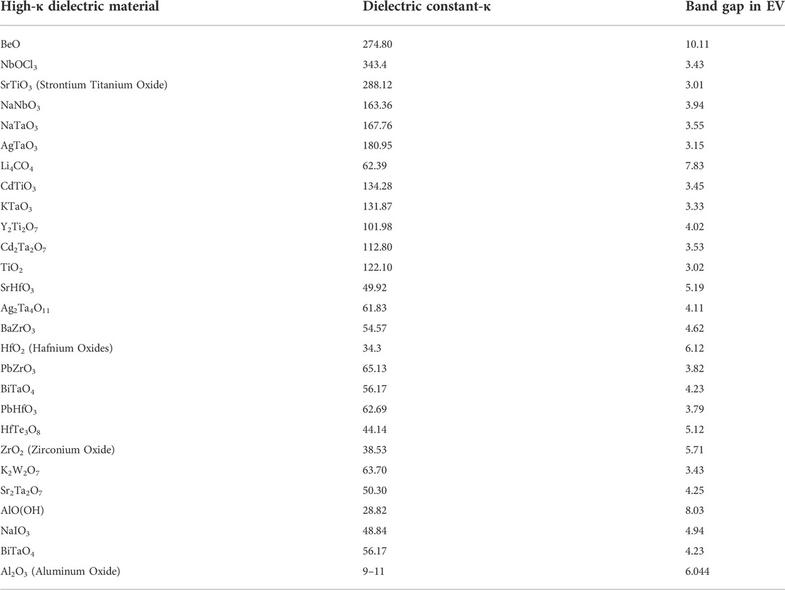
TABLE 1. List of High-κ dielectrics with their dielectric constants and band gap [2].
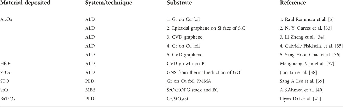
TABLE 2. High-κ dielectric on graphene.
An absolute high-κ dielectric should have both a high dielectric constant and a high band gap.
So, why do we need to amalgamate these materials with graphene? There is a restriction in normal complementary metal oxide semiconductor (CMOS) scaling mechanics. Enhancement of the performance of field-effect transistors is required. For that reason, restructuring and recasting the structure of the transistors are maintained by amalgamating novel dielectric insulators with epitaxial graphene. Scaling of Si transistors forms high leakage currents in the SiO₂ gate oxides. So, dielectric materials of high permittivity are needed [21]. That is why high-κ dielectrics such as hafnium oxide (k = 34), aluminum oxide, (k = 9), and ZrO₂ (k = 38) are explored [22]. High-κ dielectrics are used in graphene-based electronics due to lower Coulombic scattering of charge carriers and increased carrier mobility [23]. Challenges that are caused by integration with Si-based technology are mentioned [24]:
1. Appropriate band gap and permittivity with band arrangement for high-κ dielectrics on Si.
2. Interfacial stability at high-κ/Si
3. Gate source voltage instability causing low performance of devices.
4. Dielectric breakdown is a global issue in which dielectric material no longer has its insulating properties when receiving a high electric field for a long time.
The best-known example of dielectric breakdown is the electrical storm in which lighting is produced. Here, clouds/atm. air/earth forms an electrode/insulator/electrode system; in this system, when the potential difference between an electrically charged cloud and the earth reaches its limit, a sudden electrostatic discharge toward earth takes place. This is because the dielectric breakdown phenomena occurred naturally. When this electrical discharge vanishes, the insulating properties of air are reinstalled as shown in Figure 1H.
The mobility of graphene can be enhanced by up to 22% by providing an appropriate layer of nucleation by atomic layer deposition (ALD) [22]. If graphene is covered by multilayers of high-κ dielectric then a small degradation of graphene’s electronic and structural properties occurs. High-quality films are grown by ALD. These films are grown for gate dielectrics, and these are grown at a temperature below 300°C [26]. ALD is a water-based technique which means graphene must permit surface preparation processes that will permit the depositing of the uniform dielectric film. The ALD technique is highly reproducible (see Figures 1A–F).
Many other synthesis techniques such as molecular beam epitaxy and pulsed laser deposition technique are used for the oxide growth on any type of graphene. MBE technique is discussed later.
The purpose was to grow SrTiO3 on a graphene substrate using the molecular beam epitaxy technique. The sample was prepared before loading into the MBE chamber. Substrates of highly oriented pyrolytic graphite were prepared first by mechanical cleavage to expose a clean surface before loading in the MBE chamber. A base pressure of 6 *10−10 Torr was created in the chamber. The next step was to remove the surface adsorbates. To attain that, the sample needed to be annealed at 600°C for 30 min. Sr was evaporated using the growth rate from 2 to 100 Å/min. Ti was deposited from an electron-beam evaporator with a growth rate of approximately 1 Å/min. SrO was deposited to grow to a thickness of up to 3 nm. It was grown by evaporation and co-deposition of Sr and Ti in the presence of molecular oxygen SrO. The morphology of the surface obtained and thickness of the grown film were characterized using atomic force microscopy (AFM). Crystal structure and orientation was determined using two important techniques, RHEED and XRD [40].
From the previous sections of this review article, we got to know the exceptional physical properties of graphene, the basics of high-κ dielectric materials, and the challenges that arise with their integration with Si-based technology. Production of graphene in a large area is needed for the realization of graphene-based devices and the capability to amalgamate graphene with highly insulating thin films that act as gate dielectrics in field-effect transistors [22]. An attractive application of graphene is the field-effect transistor devices. These applications need the amalgamation of graphene into a composition that contains very thin dielectric layers. So, it is essential to amalgamate graphene with oxides to perceive the wide spectrum of its electronics applications as mentioned in the previous sections of this article. The properties of graphene can be regulated by overlayered oxides. For electronic devices, high-κ dielectric allows the ultra-high doping in graphene to enhance the performance of field-effect transistors which are based on graphene [22, 27, 28]. However, thermal fluctuation is another challenge of dielectric films on top of graphene, rendering manufacturing continuous dielectric/graphene interfaces tough [29]. The mobility of graphene integrated with high-κ may be restricted due to phonon scattering [30], but still, graphene-based FETs amalgamated with high-κ dielectrics perform very well [31]. This article is about fabricating layers of high-κ dielectrics on the Si face of epitaxial graphene. These materials can be used to overcome some limitations noticed in Si-based nanoelectronic devices. Saturation current and switching speed are some parameters that can be improved [32]. Very few high-κ dielectric materials have been grown on graphene until now, as shown in Table 2.
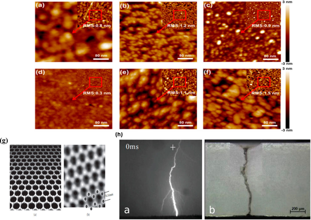
FIGURE 1. AFM images of Al₂O₃/Gr after ALD cycles, each cycle with pre-H₂O treatment at 100 °C is shown. (A) One, (B) two, (C) three, (D) four, (E) five, (F) six cycles [34], (G) structure of graphene and the high-resolution transmission electron microscopic (HRTEM) picture is shown [15], and (H) a cloud-to-earth electrical discharge through the air is shown and an Al2O3 film subjected to high electric field stress is also shown [25].
Raul Rammula et al. showed that 0.2–0.4 nm thickness of Al₂O₃ seed layers were grown using the ALD technique at 200°C. As compared to the precursor, the TMA-H₂O method of ALD did not show much uniform growth. TMA-ozone was much better as it resulted in a growth of dielectrics which was more uniform. However, it also caused some oxidation in graphene. The advantage of this ALD method was that it allowed the deposition of dielectrics on graphene in a single process [5]. Mengmeng Xiao et al. grew a very thin high-κ dielectric on graphene using the ALD process. High-quality CVD-based graphene was grown on Pt. An amorphous layer of carbon was formed on graphene because of electron-beam scanning in the chamber of a scanning electron microscope. A uniform layer of dielectric was formed as a gate dielectric for top gate graphene FETs. The gate capacitance of up to 2.63 μF per sq. cm was recorded. FET was fabricated with static carrier mobility of 2,500 sq. cm per volt per sec and negligible leakage current. The research was good for ultra-low power applications [37]. Jian Liu et al. developed nanocomposites of ZrO₂ and formed the nanosheets of graphene by an atomic layer deposition (ALD) technique. Deposition temperatures were in the range of 150–250°C. By reducing the temperature, the crystallinity was also reduced. This was a gradual decrease. The phase of the deposited sample was crystalline and amorphous at different temperatures. Both crystalline and amorphous phases were found in the ZrO₂-GNS composite at 200°C [38]. Sang A Lee et al. used CVD graphene on Cu foil for such growth using pulsed laser deposition (PLD) at 700°C. A KrF laser of 248 nm was used for plume formation at a laser density of 2 J/sq. cm, and a repetition rate of 3 Hz was used. The atomic structure was characterized by HRXRD, and thickness, by XRR. Resistive measurements, Raman spectroscopy, and TEM were also applied. Graphene induced lower resistance on STO films, establishing a crystal structure and electric conduction [39]. A. S. Ahmed et al. grew the buffer layer for oxide amalgamation. A total of 25 nm SrO/HOPG was used, resulting in SrTiO₃ film having 001 orientation. Oxygen vacancies on SrO caused charge impurity scattering, resulting in Dirac point shifting and reducing the mobility [40]. Liyan Dai et al. used the PLD technique, and highly oriented BTO films were grown. Growth was achieved on graphene, which was covered with SiO₂/Si substrates. These easily exfoliated films showed ferroelectric properties. Films followed Volmer–Weber mode. Wrinkles were obtained in graphene that showed nucleation sites at the initial stage of growth. BTO films were exfoliated using a metal Cr stressor [41].
Three steps were involved in manufacturing a graphene-based field-effect transistor, abbreviated as GFET:
There are different approaches for obtaining monolayer and few-layer graphene sheets: 1) mechanical exfoliation, 2) epitaxial growth on SiC substrate, and 3) chemical vapor deposition (CVD). The best technique is to grow monolayer/bilayer graphene on the SiC substrate epitaxially. The SiC substrate is heated up to a specific temperature to attain the desorption of Si atoms in ultra-high vacuum. The first layer of carbon is not supposed to be graphene because of the strong bonding, and no Dirac spectrum is present in it [41].
Since, now, the template is ready, the next step is to make the metal contacts and top gate. A minor value of gate capacitance is needed for some applications such as RF and digital applications. To achieve all this, one must use low leakage, thin, and uniform high-κ dielectrics for the top gate. Dielectrics for gates are synthesized preferably using the ALD technique, but deposition could also be done by thermal deposition. Now comes the challenging part as the ALD technique is water-based: The graphene plane of the base is hydrophobic, so it is difficult to deposit oxides such as high-κ dielectrics mentioned in the previous sections. Also, graphene’s surface is chemically inert, so it is more difficult to grow oxides on pristine defect-free graphene. The solution is to functionalize the sample of graphene to make it more reactive, for example, using NO2 or O3 [41].
This section discusses the third step that has not yet been discussed in this article; it is the most important one. A simple method to make contact with graphene involves patterning which includes masking to transfer the pattern. This is achieved by a method called electron-beam lithography. Ti/Au, Cr/Au, Cr/Pt, Ni, and Co are normal metals used for making contact with graphene [42].
SrO layers were fabricated on a graphene template by different deposition techniques as discussed previously. Now, to understand the effect of these layers on the electrical performance of graphene, some exfoliated SLG devices were fabricated on the SiO2(300 nm)/Si substrate. Before performing in situ electrical measurements, carrier density tuning was required. That was done using electron-beam lithography. Using the EBL technique, gold (Au) electrodes were patterned and a doped Si substrate was used as a back gate for tuning carrier density. Devices were then placed inside the UHV chamber for annealing at 100°C for 1 h. SrTiO3 was deposited on graphene at room temperature. The growth rate used was 3 Å/min. Initially, the Dirac point (i.e., resistance maximum) was observed at the gate voltage of −5 V obtained through the four-probe resistance vs. the gate voltage curve. The slope of conductivity vs. gate voltage (VG) curve shows the field-effect mobility, which was 3,050 cm2/Vs. The Dirac point shifted to a value more negative than −90 V after deposition of 2 ML of SrO (3 Å/min). SrO has oxygen vacancies, and these vacancies were like charged impurities. If we assume that each oxygen vacancy donates two electrons and carrier density varies, each volt shift of the Dirac point corresponds to one vacancy per 42,000 oxygen atoms in 2 ML SrO. Future studies should focus on increasing mobility by increasing the SrO film quality through the reduction of oxygen vacancies and structural defects [40].
Now we know about graphene and its electronic band structure. Because of its gapless electronic bands, the gate control is more challenging in comparison to its high off-state leakage currents for the fabrication of graphene-based transistors [42]. In the semiconductor industry, challenges for the size of MOSFETs are enhancing the importance of upcoming materials and devices which might improve the performance of MOSFET. This purpose requires material such as graphene with such electronic properties as discussed previously in this article. In this review article, we explored the challenges of high-κ dielectric materials on graphene [42]. Here, in this review article, it is mentioned that the structural and electronic properties of graphene change based on the choice of dielectric material growth on graphene and deposition conditions for film growth. ALD depositions of Al₂O₃, HfO₂, ZrO₂, and PLD depositions of STO, BTO, and MBE growth of SrO were shown. The work in this article provides the building block for dielectric gate and/or tunnel barrier engineering that might help in the fabrication of graphene-based transistors in the future. However, most of the graphene used until now is CVD-based graphene. More well-defined growth could be maintained by using epitaxial graphene as a future template. A huge amount of regular work in the direction of the growth of diverse oxides has already been done. However, the growth of high-quality oxide layers on graphene is proving to be a serious issue. CVD-grown graphene is a very cost-effective and popular method. Most of the work is done on traditional CVD-grown graphene, which is polycrystalline, and exfoliated graphene which has limited-size flakes. As we previously discussed, both types of graphene need to be transferred onto some insulating substrate such as Si/SiO₂. Also, this transferring process results in further defects/wrinkling in graphene. In such cases, the template does not act as an ideal substrate for the epitaxial growth of oxides due to inherent defects and multiple domains oriented in random directions and of limited size. This reduces the performance of the device due to haphazard oriented domains of graphene and adulteration at the interface. Ideally, if we want graphene as a growth template for epitaxial growth of oxides, then it should be single crystalline, should have homogeneous thickness over a large area (mm scale), and should not need to be transferred. Si sublimation from SiC and subsequent recombination of carbon atoms leading to epitaxial graphene has emerged as one of the best methods to achieve large-area single crystalline graphene with controlled layered thickness.
The quality of manufactured high-κ dielectric films on graphene is analogous to the best quality of high-κ films on Si, and it has great prospects for future graphene application in electronics. Here, in this review article, it was noted that the structural and electronic properties of epitaxial graphene change based on the choice of dielectric material growth on graphene and deposition conditions for film growth. There is only minimal degradation in the structural properties of epitaxial graphene. The work shown in this article is the building block for dielectric gate and/or tunnel barrier engineering that might provide help in the fabrication of graphene-based transistors in the future.
Author made a substantial, direct, and intellectual contribution to the work and approved it for publication.
I thank the Academy of Scientific and Innovative Research (AcSIR), India, and CSIR-NPL, India. I am also thankful for the financial support of the CSIR fellowship (no. 31/001(0633)/2020-EMR-I).
The author declares that the research was conducted in the absence of any commercial or financial relationships that could be construed as a potential conflict of interest.
All claims expressed in this article are solely those of the authors and do not necessarily represent those of their affiliated organizations, or those of the publisher, the editors, and the reviewers. Any product that may be evaluated in this article, or claim that may be made by its manufacturer, is not guaranteed or endorsed by the publisher.
1. Park J, Lee J, Choi JH, Hwang DK, Song YW. Growth, quantitative growth analysis, and applications of graphene on γ-Al2O3 catalysts. Sci Rep (2015) 5:11839–12. doi:10.1038/srep11839
2. Yim K, Yong Y, Lee J, Lee K, Nahm HH, Yoo J, et al. Novel high- κ dielectrics for next-generation electronic devices screened by automated ab initio calculations. NPG Asia Mater (2015) 7:e190–6. doi:10.1038/am.2015.57
3. Ak G. Graphene: Status and prospects. Science (2009) 324(5934):1530–4. doi:10.1126/science.1158877
4. Lin Z, McCreary A, Briggs N, Subramanian S, Zhang K, Sun Y, et al. 2D materials advances: From large scale synthesis and controlled heterostructures to improved characterization techniques, defects and applications. 2d Mater (2016) 3(4):042001. doi:10.1088/2053-1583/3/4/042001
5. Rammula R, Aarik L, Kasikov A, Kozlova J, Kahro T, Matisen L, et al. Atomic layer deposition of aluminum oxide films on graphene. IOP Conf Ser : Mater Sci Eng (2013) 49(1):012014. doi:10.1088/1757-899X/49/1/012014
6. Vaziri S, Chen V, Cai L, Jiang Y, Chen ME, Grady RW, et al. Ultrahigh doping of graphene using flame-deposited moo3. IEEE Electron Device Lett (2020) 41(10):1592–5. doi:10.1109/LED.2020.3018485
7. Min JH, Li KH, Kim YH, Kang CH, Kim KH, Lee K., et al. Toward large-scale Ga2O3Membranes via quasi-van der Waals epitaxy on epitaxial graphene layers. ACS Appl Mater Inter (2021) 13(11):13410–8. doi:10.1021/acsami.1c01042
8. Mayorov AS, Gorbachev RV, Morozov SV, Britnell L, Jalil R, Ponomarenko LA, et al. Micrometer-scale ballistic transport in encapsulated graphene at room temperature. Nano Lett (2011) 11(6):2396–9. doi:10.1021/nl200758b
9. Lee C, Wei X, Kysar JW, Hone J. Measurement of the elastic properties and intrinsic strength of monolayer graphene. Science (2008) 321(5887):385–8. doi:10.1126/science.1157996
10. Sinclair RC, Suter JL, Coveney PV. Micromechanical exfoliation of graphene on the atomistic scale. Phys Chem Chem Phys (2019) 21(10):5716–22. doi:10.1039/c8cp07796g
11. Wang X, You H, Liu F, Li M, Wan L, Li S, et al. Large-scale synthesis of few-layered graphene using CVD. Chem Vap Deposition (2009) 15(1–3):53–6. doi:10.1002/cvde.200806737
12. De Heer WA, Berger C, Wu X, First PN, Conrad EH, Li X, et al. Epitaxial graphene. Solid State Commun (2007) 143(1–2):92–100. doi:10.1016/j.ssc.2007.04.023
13. De Heer WA, Berger C, Ruan M, Sprinkle M, Li X, Hu Y, et al. Large area and structured epitaxial graphene produced by confinement controlled sublimation of silicon carbide. Proc Natl Acad Sci U S A (2011) 108(41):16900–5. doi:10.1073/pnas.1105113108
15. Sur UK. Graphene: A rising star on the horizon of materials science. Int J Electrochem (2012) 2012:1–12. doi:10.1155/2012/237689
16. Wang D, Chen G, Li C, Cheng M, Yang W, Wu S, et al. Thermally induced graphene rotation on hexagonal boron nitride. Phys Rev Lett (2016) 116(12):126101–6. doi:10.1103/PhysRevLett.116.126101
17. Ge S, Habib KMM, De A, Barlas Y, Wickramaratne D, Neupane MR, et al. Interlayer transport through a graphene/rotated boron nitride/graphene heterostructure. Phys Rev B (2017) 95(4):045303–9. doi:10.1103/PhysRevB.95.045303
18. Gigliotti J “Integrated dielectrics for protection and gating of epitaxial graphene devices”, (2017).
19. Kingon AI, Maria J-P, Streiffer SK. Alternative dielectrics to silicon dioxide for memory and logic devices. Nature (2000) 406:1032–8. doi:10.1038/35023243
20. Lee CH, Hur SH, Shin YC, Choi JH, Park DG, Kim K. Charge-trapping device structure of Si O2 SiNhigh-k dielectric Al2 O3 for high-density flash memory. Appl Phys Lett (2005) 86(15):152908–3. doi:10.1063/1.1897431
21. Wilk GD, Wallace RM, Anthony JM. High-κ gate dielectrics: Current status and materials properties considerations. J Appl Phys (2001) 89(10):5243–75. doi:10.1063/1.1361065
22. Robinson JA, LaBella M, Trumbull KA, Weng X, Cavelero R, Daniels T, et al. Epitaxial graphene materials integration: Effects of dielectric overlayers on structural and electronic properties. ACS Nano (2010) 4(5):2667–72. doi:10.1021/nn1003138
23. Chen F, Xia J, Tao N. Ionic screening of charged-impurity scattering in graphene. Nano Lett (2009) 9(4):1621–5. doi:10.1021/nl803922m
24. He G, Zhu L, Sun Z, Wan Q, Zhang L. Integrations and challenges of novel high-k gate stacks in advanced CMOS technology. Prog Mater Sci (2011) 56(5):475–572. doi:10.1016/j.pmatsci.2011.01.012
25. Palumbo F, Wen C, Lombardo S, Pazos S, Aguirre F, Eizenberg M, et al. A review on dielectric breakdown in thin dielectrics: Silicon dioxide, high-k, and layered dielectrics. Adv Funct Mater (2020) 30(18):1900657–26. doi:10.1002/adfm.201900657
26. Kim J, Park SY, Kim HC, Cho K, Vogel EM, Kim MJ, et al. Conformal Al2O3 dielectric layer deposited by atomic layer deposition for graphene-based nanoelectronics. Appl Phys Lett (2008) 92(20):203102–4. doi:10.1063/1.2928228
27. Addou R, Dahal A, Batzill M. Growth of a two-dimensional dielectric monolayer on quasi-freestanding graphene. Nat Nanotechnol (2013) 8(1):41–5. doi:10.1038/nnano.2012.217
28. Farmer DB, Chiu HY, Lin YM, Jenkins KA, Xia F, Avouris P. Utilization of a buffered dielectric to achieve high field-effect carrier mobility in graphene transistors. Nano Lett (2009) 9(12):4474–8. doi:10.1021/nl902788u
29. Fallahazad B, Lee K, Lian G, Kim S, Corbet CM, Ferrer DA, et al. Scaling of Al 2O 3 dielectric for graphene field-effect transistors. Appl Phys Lett (2012) 100(9):093112–4. doi:10.1063/1.3689785
30. Konar A, Fang T, Jena D, “Effect of high-K dielectrics on charge transport in graphene,” (2009), doi:10.1103/PhysRevB.82.115452
31. Lemme MC, Echtermeyer TJ, Baus M, Kurz H. A graphene field-effect device. IEEE Electron Device Lett (2007) 28(4):282–4. doi:10.1109/LED.2007.891668
32. Franklin AD. Nanomaterials in transistors: From high-performance to thin-film applications. Science (2015) 349:aab2750–6249. doi:10.1126/science.aab2750
33. Garces NY, Wheeler VD, Hite JK, Jernigan GG, Tedesco JL, Nepal N, et al. Epitaxial graphene surface preparation for atomic layer deposition of Al2O3. J Appl Phys (2011) 109(12):124304–6. doi:10.1063/1.3596761
34. Zheng L, Cheng X, Cao D, Wang G, Wang Z, Xu D, et al. Improvement of Al2O3 films on graphene grown by atomic layer deposition with Pre-H2O treatment. ACS Appl Mater Inter (2014) 6(10):7014–9. doi:10.1021/am501690g
35. Fisichella G, Schiliro E, Di Franco S, Fiorenza P, Lo Nigro R, Roccaforte F, et al. Interface electrical properties of Al2O3 thin films on graphene obtained by atomic layer deposition with an in situ seedlike layer. ACS Appl Mater Inter (2017) 9(8):7761–71. doi:10.1021/acsami.6b15190
36. Chae SH, Yu WJ, Bae JJ, Duong DL, Perello D, Jeong HY, et al. Transferred wrinkled Al2O3 for highly stretchable and transparent graphene-carbon nanotube transistors. Nat Mater (2013) 12(5):403–9. doi:10.1038/nmat3572
37. Xiao M, Qiu C, Zhang Z, Peng L. Atomic-layer-deposition growth of an ultrathin HfO 2 film on graphene. ACS Appl Mater Inter (2017) 9(39):34050–6. doi:10.1021/acsami.7b09408
38. Liu J, Meng X, Hu Y, Geng D, Norouzi M, Cai M, et al. Controlled synthesis of Zirconium Oxide on graphene nanosheets by atomic layer deposition and its growth mechanism. Carbon N Y (2012) 52:74–82. doi:10.1016/j.carbon.2012.09.007
39. Lee SA, Hwang JY, Km ES, Kim SW, Choi WS. Highly oriented SrTiO3 thin film on graphene substrate. ACS Appl Mater Inter (2017) 9(4):3246–50. doi:10.1021/acsami.6b12258
40. Ahmed AS, Wen H, Ohta T, Pinchuk IV, Zhu T, Beechem T, et al. Molecular beam epitaxy growth of SrO buffer layers on graphite and graphene for the integration of complex oxides. J Cryst Growth (2016) 447:5–12. doi:10.1016/j.jcrysgro.2016.04.057
41. Dai L, Niu G, Zhao J, Zhao H, Liu Y, Wang Y, et al. Toward van der Waals epitaxy of transferable ferroelectric barium titanate films: Via a graphene monolayer. J Mater Chem C Mater (2020) 8(10):3445–51. doi:10.1039/c9tc06454k
Keywords: graphene, van der Waals epitaxy (VDWE), heterostructures, high-κ dielectrics, Al2O3
Citation: Khanna S (2022) Amalgamation of high-κ dielectrics with graphene: A catalyst in the orbit of nanoelectronics and material sciences. Front. Phys. 10:1064929. doi: 10.3389/fphy.2022.1064929
Received: 08 October 2022; Accepted: 10 November 2022;
Published: 30 November 2022.
Edited by:
Zeinab Ramezani, University of Miami, United StatesReviewed by:
Husien Salama, University of Connecticut, United StatesCopyright © 2022 Khanna. This is an open-access article distributed under the terms of the Creative Commons Attribution License (CC BY). The use, distribution or reproduction in other forums is permitted, provided the original author(s) and the copyright owner(s) are credited and that the original publication in this journal is cited, in accordance with accepted academic practice. No use, distribution or reproduction is permitted which does not comply with these terms.
*Correspondence: Sadhak Khanna, c2FkaGFrLm5wbDIwakBhY3Npci5yZXMuaW4=
Disclaimer: All claims expressed in this article are solely those of the authors and do not necessarily represent those of their affiliated organizations, or those of the publisher, the editors and the reviewers. Any product that may be evaluated in this article or claim that may be made by its manufacturer is not guaranteed or endorsed by the publisher.
Research integrity at Frontiers
Learn more about the work of our research integrity team to safeguard the quality of each article we publish.