 M. Amir Bazrafshan
 Farhad Khoeini
- Department of Physics, University of Zanjan, Zanjan, Iran
The Seebeck coefficient is an important quantity in determining the thermoelectric efficiency of a material. Phosphorene is a two-dimensional material with a puckered structure, which makes its properties anisotropic. In this work, a phosphorene nanodisk (PDisk) with a radius of 3.1 nm connected to two zigzag phosphorene nanoribbons is studied, numerically, by the tight-binding and non-equilibrium Green’s function (NEGF) methods in the presence of transverse and perpendicular electric fields. Our results show that the change in structure from a zigzag ribbon to a disk form creates an energy gap in the structure, such that for a typical nanodisk with a radius of 3.1 nm, the size of the energy gap is 3.88 eV. Besides, with this change, the maximum Seebeck coefficient increases from 1.54 to 2.03 mV/K. Furthermore, we can control the electron transmission and Seebeck coefficients with the help of the electric fields. The numerical results show that with the increase of the electric field, the transmission coefficient decreases and the Seebeck coefficient changes. The effect of a perpendicular electric field on the Seebeck coefficient is weaker than a transverse electric field. For an applied transverse electric field of 0.3 V/nm, the maximum Seebeck coefficient enhances to 2.09 mV/K.
Introduction
Thermoelectrics is an active field in nanotechnology for converting thermal energy into electricity. Researchers are trying to enhance the thermoelectric efficiency of various materials. In recent decades, owing to high-precision tools, engineering the shape of materials at nanoscales where quantum mechanical effects play a major role in determining the physical properties [1] is not just a dream.
After realizing graphene in 2004 [2], the world of two-dimensional (2D) materials attracted the attention of researchers, since they possess extraordinary properties.
Phosphorene, the two-dimensional form of black phosphorus [3, 4], is one of the materials that is of interest in the scientific community. Owing to its specific geometry, the physical properties of the phosphorene monolayer are not isotropic and are depend on the direction [3–8]. Phosphorene is proposed for a variety of applications such as transistors, batteries, water splitting, sensors, and optoelectronic applications [9–12].
The chemical stability of black phosphorus is better than that of red and white ones [1]. Phosphorene is a direct bandgap semiconductor (>1.5 eV) with high carrier mobility [8, 13–16]. The lattice thermal conductivity for phosphorene in the zigzag direction is higher than it is in the armchair direction [15, 17]. Although, phosphorene is unstable when exposed to air, to overcome this challenge, it is usually sandwiched between other materials [16]. Tailoring nanostructures can change their physical properties, and for phosphorene, despite it being an intrinsic semiconductor, its zigzag nanoribbon has a metallic behavior [18].
Quantum confinement effects become important at the nanoscale level and can hence help control the physical properties of a material, such as the Seebeck coefficient, which is essential for thermoelectric performance [19–21]. In this study, we investigate the electronic transport properties of a phosphorene nanodisk with a radius of R = 3.1 nm connected to two zigzag phosphorene nanoribbons (ZPNRs) with 12 atoms widthwise (12-ZPNR), as shown in Figure 1. We use the tight-binding and the nonequilibrium Green’s function methods for this goal. As reported in [22, 23], the five-hopping TB model is accurately reconstructed near the Fermi bands for the phosphorene monolayer. We also applied two electric fields perpendicular to the transport direction of up to 0.3
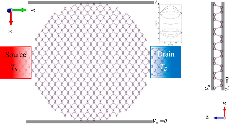
FIGURE 1. A phosphorene nanodisk with a radius of 3.1 nm connected to the two 12 ZPNR leads. The transport direction is along the y-axis. The source and drain leads act as the hot bath and cold bath, respectively. The TB electronic band structure of the 12-ZPNR is also shown on top of the drain lead. Transverse (
This article is arranged as follows: in the next section, we describe the model and method with a brief introduction to the TB and NEGF methods. In the section after that, the results and discussion are presented. In the last section, we conclude our study.
Model and method
The system consists of a phosphorene disk connected to two metallic leads, as shown in Figure 1. Two zigzag phosphorene ribbon leads are labeled as the source and drain. Besides, the central region between the two leads is a nanodisk device which contains 798 atoms.
The width of the ZPNR leads includes 12 atoms. Phosphorene is a semiconductor, but cutting it into a zigzag nanoribbon turns it into a metal as mentioned in [18, 25, 26] and can be seen from the TB electronic band structure shown in Figure 1.
The electronic and transport behaviors of the system are described by the TB Hamiltonian:
where
Moreover, the electric fields are only applied to the nanodisk, i.e., the device section. Therefore, the electrodes do not feel any electric field. The calculation method is available in [29]. To study the transport properties, the TB Hamiltonians are implemented in the NEGF formalism. The retarded Green’s function can be evaluated as follows [30]:
where
The spectral density operator is given by
The transmission probability for the electron can be obtained as follows:
Besides, the local density of state (LDOS) for a given atom (indicated by index i) can be derived by evaluating
Now, one can evaluate the electronic conductance, g; the Seebeck coefficient, S; and the electronic thermal conductance,
The elementary charge is indicated by
with
Results and discussion
The electronic transport properties and the Seebeck coefficient are studied in a phosphorene nanodisk with a radius of R = 3.1 nm with the help of the TB method and NEGF formalism. As mentioned earlier, phosphorene is not an isotropic structure.
The electronic conductance in the zigzag direction is about an order of magnitude lower than the armchair direction, as reported in [6]. In contrast to electronic conductance, the phononic conductance in the zigzag direction is about 40% higher than that in the armchair direction. As one can see in Eqs. 6, 7, the Seebeck coefficient is calculated based on the transmission coefficient. Hence, to have a larger S, a zero transmission coefficient with respect to the Fermi energy is of high importance (the wider energy gap, the higher S) or a transmission coefficient with sharp peaks followed by low values. Therefore, we first investigate the transmission coefficient. In the absence of any electric field, the ZPNR is a metal, as evidenced by its electronic band structure (Figure 1) and the transmission spectrum (thick red line in the panels of Figure 2). In the case of the nanodisk, the structure has an energy gap of 3.88 eV, as shown in Figure 2A (magenta line). With the increase of the transverse electric field strength (blue line for
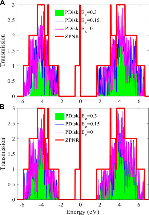
FIGURE 2. Transmission spectra of the phosphorene nanodisk: (A) in the presence of various
We note that colors are preserved in all figures respect to the structures and studied electric fields. The behavior of the transmission coefficient is important in determining the Seebeck coefficient. On the other hand, based on the formalism used in this work, at a fixed temperature, the overall transport coefficient is important in determining the Seebeck coefficient, as the integral in Eq. 7 says.
It is important to know what states are present in the device, so that the energy levels are plotted against the state index by solving the eigenvalue problem for each state in the device [34], as shown in Figure 3A. The bulk energy gap in the device, based on these energy levels, is ∼1.66 eV, close to the phosphorene bandgap, indicating that from the electronic energy gap point of view, the behavior of this nanodisk is almost close to that of a single-layer phosphorene.
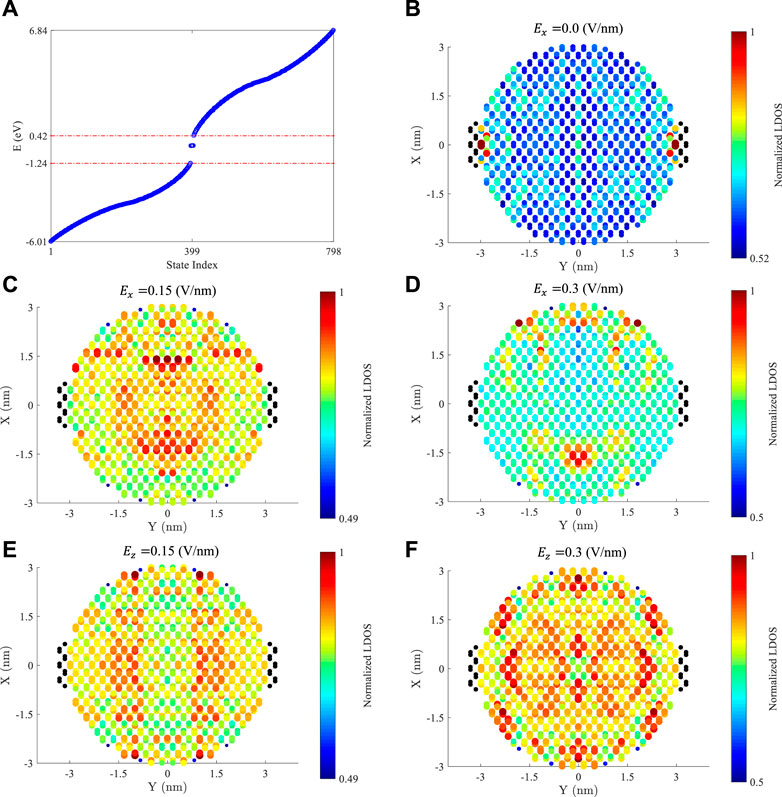
FIGURE 3. (A) Energy levels vs. state index for the PDisk. (B) Normalized LDOS for the PDisk in the absence of an electric field, (C)
In the next step, we take a look into the local DOS. The normalized LDOS is obtained respect to the highest LDOS in the particular system. Figure 3B presents the normalized LDOS of the PDisk with no bias. The LDOS shows that atoms in the upper and lower layers of the puckered structure of phosphorene have different local electron densities, and according to the central point of the device, there is a mirror symmetric behavior from the LDOS point of view in all directions. Here, we arrange the structure according to the origin of the coordination system (0, 0, 0). The high LDOS states are located where the electrodes are connected to the device. In the disk region, the LDOS distribution is not too different, a clue of lower localization and thus of better conductivity. Higher localized states can enhance the Seebeck coefficient by reducing the contribution of electrons in conductivity. In this case, the high LDOS states in the path of entry and exit of the electrons in the system suppresses the participation of electrons in their related properties. Figure 3C shows the effect of an electric field of
The path for moving an electron between the two leads is not straight, since high LDOS atoms are surrounded by relatively low LDOS ones, making it an uneven path. It should be noted that atoms at the lowest x-coordination do not experience electric potential, but the ones at the highest x-coordination experience the highest electric potential, so the atoms between these hypothetical lines feel a relative electric potential with respect to their position.
For
The LDOS in the presence of perpendicular electric fields of 0.15 and 0.3 V/nm are presented, respectively, in the panels of Figure 3E, F. For the electric fields, the LDOS distribution is mirror symmetric with respect to the center, similar to the system without applying an electric field.
The Seebeck coefficient is plotted in Figure 4 for the leads and the transport system and in the presence of the different applied electric fields. As we mentioned earlier, more suppression of the overall transmission coefficient, especially close to the Fermi level of the system can lead to a higher Seebeck coefficient.
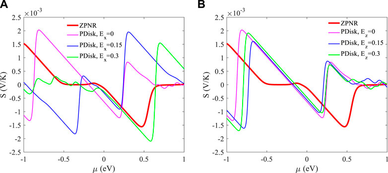
FIGURE 4. Seebeck coefficient behavior vs. chemical potential for the 12-ZPNR and various electric field strengths applied along the (A) x-axis and (B) z-axis of the PDisk. Coordinate axes are shown in Figure 1. The temperature is 300 K. The unit for the electric fields is V/nm.
The Seebeck coefficient of the leads is small, which is a consequence of metallicity (thick red line in both and panels in Figures 4A, B). For an applied transverse electric field (blue line in Figure 4A), one can see that a moderate electric field,
This behavior is also evident in the case of a perpendicular electric field (Figure 4B), although the Seebeck coefficient does not reach to the case in the absence of an electric field. The sign change of the Seebeck coefficient is attributed to the change of the carrier type, meaning that the high S for
From a thermoelectric point of view, the square of the Seebeck coefficient is important when calculating the thermoelectric efficiency [35]. The maximum absolute value of S in the absence of an electric field is ∼2.03 mV/K at a chemical potential
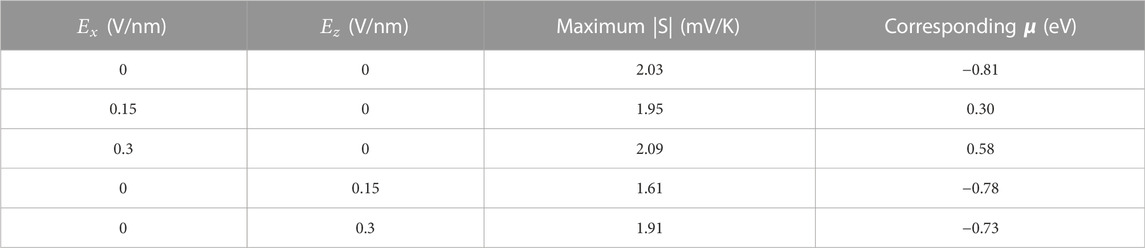
TABLE 1. Seebeck coefficient and corresponding chemical potential in the presence of different electric fields.
Conclusion
In this work, we have studied the transmission coefficient and the Seebeck coefficient of a phosphorene nanodisk with a radius of 3.1 nm within the framework of the five-hopping TB model and with the help of NEGF formalism. According to our numerical results, engineering phosphorene to a nanodisk at the nanoscale increases the Seebeck coefficient to 2.03 mV/K and induces an energy gap of 3.88 eV. Our numerical results have shown that with an increase of the magnitude of electric field, the transmission coefficient decreases and the Seebeck coefficient changes. Moreover, an electric field perpendicular to the disk surface has a smaller impact on the Seebeck coefficient than a transverse electric field. A transverse electric field with the strength of 0.3 V/nm enhances the Seebeck coefficient to 2.09 mV/K. These results can help in the design of phosphorene-based materials in thermoelectrics.
Data availability statement
The original contributions presented in the study are included in the article/supplementary material; further inquiries can be directed to the corresponding author.
Author contributions
M-AB carried out the simulations. M-AB and FK analyzed the data and prepared the manuscript. FK supervised the project and revised the final manuscript. All authors read and approved the final manuscript.
Conflict of interest
The authors declare that the research was conducted in the absence of any commercial or financial relationships that could be construed as a potential conflict of interest.
Publisher’s note
All claims expressed in this article are solely those of the authors and do not necessarily represent those of their affiliated organizations, or those of the publisher, editors, and reviewers. Any product that may be evaluated in this article, or claim that may be made by its manufacturer, is not guaranteed or endorsed by the publisher.
References
1. Majumdar A. Thermoelectricity in semiconductor nanostructures. Science (2004) 303:777–8. doi:10.1126/science.1093164
2. Novoselov KS, Geim AK, Morozov SV, Jiang D, Zhang Y, Dubonos SV, et al. Electric field effect in atomically thin carbon films. Science (2004) 306:666–9. doi:10.1126/science.1102896
3. Qin G, Hu M. Thermal transport in phosphorene. Small (2018) 14:1702465. doi:10.1002/smll.201702465
4. Jing Y, Zhang X, Zhou Z. Phosphorene: What can we know from computations? Wiley Interdiscip Rev Comput Mol Sci (2016) 6:5–19. doi:10.1002/wcms.1234
5. Boutahir O, Lakhlifi S, Abdelkader SAA, Boutahir M, Rahmani A, Chadli H, et al. Force-constant model for the vibrational modes in black-phosphorene and phosphorene nanoribbons (PNRs). Phys E Low-dimensional Syst Nanostructures (2021) 132:114757. doi:10.1016/j.physe.2021.114757
6. Fei R, Faghaninia A, Soklaski R, Yan J-A, Lo C, Yang L. Enhanced thermoelectric efficiency via orthogonal electrical and thermal conductances in phosphorene. Nano Lett (2014) 14:6393–9. doi:10.1021/nl502865s
7. Hong Y, Zhang J, Cheng Zeng X. Thermal transport in phosphorene and phosphorene-based materials: A review on numerical studies. Chin Phys. B (2018) 27:036501. doi:10.1088/1674-1056/27/3/036501
8. Zhang Y-Y, Pei Q-X, Jiang J-W, Wei N, Zhang Y-W. Thermal conductivities of single- and multi-layer phosphorene: A molecular dynamics study. Nanoscale (2016) 8:483–91. doi:10.1039/c5nr05451f
9. Batmunkh M, Bat-Erdene M, Shapter JG. Phosphorene and phosphorene-based materials – prospects for future applications. Adv Mater (2016) 28:8586–617. doi:10.1002/adma.201602254
10. Carvalho A, Wang M, Zhu X, Rodin AS, Su H, Castro Neto AH. Phosphorene: From theory to applications. Nat Rev Mater (2016) 1:16061. doi:10.1038/natrevmats.2016.61
11. Watts MC, Picco L, Russell-Pavier FS, Cullen PL, Miller TS, Bartuś SP, et al. Production of phosphorene nanoribbons. Nature (2019) 568:216–20. doi:10.1038/s41586-019-1074-x
12. Kou L, Chen C, Smith SC. Phosphorene: Fabrication, properties, and applications. J Phys Chem Lett (2015) 6:2794–805. doi:10.1021/acs.jpclett.5b01094
13. Zhou H, Cai Y, Zhang G, Zhang YW. Thermoelectric properties of phosphorene at the nanoscale. J Mater Res (2016) 31:3179–86. doi:10.1557/jmr.2016.333
14. Zhang J, Hong Y, Liu M, Yue Y, Xiong Q, Lorenzini G. Molecular dynamics simulation of the interfacial thermal resistance between phosphorene and silicon substrate. Int J Heat Mass Transf (2017) 104:871–7. doi:10.1016/j.ijheatmasstransfer.2016.08.021
15. Hong Y, Zhang J, Huang X, Zeng XC. Thermal conductivity of a two-dimensional phosphorene sheet: A comparative study with graphene. Nanoscale (2015) 7:18716–24. doi:10.1039/c5nr03577e
16. Mahdavifar M, Shekarforoush S, Khoeini F. Tunable electronic properties and electric-field-induced phase transition in phosphorene/graphene heterostructures. J Phys D Appl Phys (2021) 54:095108. doi:10.1088/1361-6463/abcbbe
17. Ong Z-Y, Cai Y, Zhang G, Zhang Y-W. Strong thermal transport anisotropy and strain modulation in single-layer phosphorene. J Phys Chem C (2014) 118:25272–7. doi:10.1021/jp5079357
18. Wu Q, Shen L, Yang M, Cai Y, Huang Z, Feng YP. Electronic and transport properties of phosphorene nanoribbons. Phys Rev B - Condens Matter Mater Phys (2015) 92:035436. doi:10.1103/physrevb.92.035436
19. Tan X, Liu H, Wen Y, Lv H, Pan L, Shi J, et al. Optimizing the thermoelectric performance of zigzag and chiral carbon nanotubes. Nanoscale Res Lett (2012) 7:116. doi:10.1186/1556-276x-7-116
20. Zebarjadi M, Esfarjani K, Dresselhaus MS, Ren ZF, Chen G. Perspectives on thermoelectrics: From fundamentals to device applications. Energy Environ. Sci. (2012) 5:5147–62. doi:10.1039/c1ee02497c
21. Chakraborty S, Maiti SK. Controlled thermoelectric performance in a nanojunction: A theoretical approach. J Appl Phys (2020) 127:024302. doi:10.1063/1.5109854
22. Rudenko AN, Katsnelson MI. Quasiparticle band structure and tight-binding model for single- and bilayer black phosphorus. Phys Rev B (2014) 89:201408. doi:10.1103/physrevb.89.201408
23. Ezawa M. Topological origin of quasi-flat edge band in phosphorene. New J Phys (2014) 16:115004. doi:10.1088/1367-2630/16/11/115004
24. Ma R, Geng H, Deng WY, Chen MN, Sheng L, Xing DY. Effect of the edge states on the conductance and thermopower in zigzag phosphorene nanoribbons. Phys Rev B (2016) 94:125410. doi:10.1103/physrevb.94.125410
25. Yan JY, Li J, Lei LM, Wang JH. The influence of strain on the energy band structures of phosphorene nanoribbons. Phys Lett Sect A Gen Solid State Phys (2017) 381:2827–31. doi:10.1016/j.physleta.2017.06.044
26. Carvalho A, Rodin AS, Castro Neto AH. Phosphorene nanoribbons. Phosphorene Nanoribbons, Epl (2014) 108:47005. doi:10.1209/0295-5075/108/47005
27. Thakur T, Szafran B. Aharonov-bohm oscillations in phosphorene quantum rings: Mass anisotropy compensation by confinement potential. Phys Rev B (2022) 105:165309. doi:10.1103/physrevb.105.165309
28. Abdi M, Astinchap B, Khoeini F. Electronic and Thermodynamic Properties of Zigzag MoS2/MoSe2 and MoS2/WSe2 Hybrid Nanoribbons: Impacts of Electric and Exchange Fields. Results Phys (2022) 34:105253. doi:10.1016/j.rinp.2022.105253
29. Mahdavifar M, Khoeini F. Highly tunable charge and spin transport in silicene junctions: Phase transitions and half-metallic states. Nanotechnology (2018) 29:325203. doi:10.1088/1361-6528/aac66f
30. Wu Y, Childs PA. Conductance of graphene nanoribbon junctions and the tight binding model. Nanoscale Res Lett (2011) 6:62. doi:10.1007/s11671-010-9791-y
31. Sancho MPL, Sancho JML, Rubio J. Quick iterative scheme for the calculation of transfer matrices: Application to Mo (100). J Phys F Met Phys (1984) 14:1205–15. doi:10.1088/0305-4608/14/5/016
32. Gholami Z, Khoeini F. Vacancy tuned thermoelectric properties and high spin filtering performance in graphene/silicene heterostructures. Sci Rep (2021) 11:15320. doi:10.1038/s41598-021-94842-w
33. Sivan U, Imry Y. Multichannel landauer formula for thermoelectric transport with application to thermopower near the mobility edge. Phys Rev B (1986) 33:551–8. doi:10.1103/physrevb.33.551
34. Li LL, Moldovan D, Xu W, Peeters FM. Electric- and magnetic-field dependence of the electronic and optical properties of phosphorene quantum dots. Nanotechnology (2017) 28:085702. doi:10.1088/1361-6528/aa55e8
Keywords: Green’s function, tight-binding, electron transmission, phosphorene, nanodisk
Citation: Bazrafshan MA and Khoeini F (2023) Electronic transport and thermoelectric properties of phosphorene nanodisk under an electric field. Front. Phys. 10:1063339. doi: 10.3389/fphy.2022.1063339
Received: 07 October 2022; Accepted: 12 December 2022;
Published: 04 January 2023.
Edited by:
Santanu K. Maiti, Indian Statistical Institute, IndiaCopyright © 2023 Bazrafshan and Khoeini. This is an open-access article distributed under the terms of the Creative Commons Attribution License (CC BY). The use, distribution or reproduction in other forums is permitted, provided the original author(s) and the copyright owner(s) are credited and that the original publication in this journal is cited, in accordance with accepted academic practice. No use, distribution or reproduction is permitted which does not comply with these terms.
*Correspondence: Farhad Khoeini, a2hvZWluaUB6bnUuYWMuaXI=