 Tu-Lu Liang
 Xi Cheng
 Mei Yu1,2
95% of researchers rate our articles as excellent or good
Learn more about the work of our research integrity team to safeguard the quality of each article we publish.
Find out more
ORIGINAL RESEARCH article
Front. Phys. , 19 December 2022
Sec. Optics and Photonics
Volume 10 - 2022 | https://doi.org/10.3389/fphy.2022.1029359
This article is part of the Research Topic Recent Developments in Si-based Materials and Devices View all 8 articles
In this paper, an adiabatic operation slope-loss algorithm (AO-SLA) is developed for designing efficient adiabatic waveguide tapers. The algorithm can compute the efficient adiabatic guided-wave shape of the waveguide taper. A well-studied case of an adiabatic waveguide taper is used to show how it can readily generate a guided-wave shape that gives the same mode-connection power transfer with a much shorter length compared with the linear shape. In the waveguide taper design, it is shown that the device efficiency designed with AO-SLA is better than that based on the parabolic case and the SLA case, and the adiabatic taper designed can give a broad operating bandwidth. Moreover, the adiabatic condition α for AO-SLA can be very large.
Silicon waveguides based on the silicon-on insulator (SOI) structure have attracted a large amount of attention due to their fabrication compatibility with CMOS processes, their good mode confinement, and enhanced nonlinearity. The waveguides with different cross-sections are designed to achieve different functions. Adiabatic waveguide tapers are of great importance in integrated optics applications that require broad operating bandwidth and high tolerance to fabrication variations.
The adiabatic waveguide taper is used to change the size and shape of the optical beam mode to achieve a high mode-connection power transfer efficiency (MCTE) [1] between two different waveguides. Thus, the adiabatic taper involves transferring a particular eigenmode by varying the waveguide structures from the input to output. The adiabatic condition can be achieved in the adiabatic taper design via increasing/decreasing the cross-section size of the taper slowly. The mode evolution can be regarded as lossless when the variation is slow enough. Thus, the adiabatic operation (AO) of the device can be obtained by a sufficiently long transfer structure.
A very simple way of designing the adiabatic taper is using a linear shape to join the input to the output. However, it requires a very long length of the taper and it will cause propagation losses if the device is too long. This problem will become more serious when the cross-sections of two waveguides connected by the linear taper are very different. Many other designs for the adiabatic tapers have been proposed, including exponential [2], parabolic [3], and Gaussian [4] expansion types, of which the parabolic shape is considered to be quite effective. There are also many effective designs for tapered waveguides [5–9]. For example, the tapers without mode-power loss were achieved by requiring the refractive index of the waveguide to vary in space [5–8]. Although the design is more effective in theory, this kind of tapers that varying with the refractive index are difficult to fabricate. Generally speaking, there are few cases of this kind of specially optimized design which is often very complicated and sometimes impractical. In 2014, an efficient adiabatic taper with a length of 120 μm was proposed to connect a 12 μm-wide grating coupler and a 0.5 μm-wide silicon waveguide [9]. However, they rarely introduced the details of the design and used the parabolic tapers in their later published paper [10].
In this paper, an efficient adiabatic operation slope-loss algorithm (AO-SLA) is presented for the design of adiabatic waveguide tapers. A waveguide taper was first designed by SLA [1] to obtain a better design effect and the proposed AO-SLA can use the same divisions of SLA. The design rule of each section to ensure adiabatic operation in the adiabatic waveguide taper was based on the equation proposed by Milton and Burns in 1977 [11, 12]. With AO-SLA, the details of the method, the device efficiency and the operating wavelength bandwidth of the adiabatic taper are investigated. Besides, the performance degradations due to the increase of adiabatic condition α are also analyzed, showing the robustness of AO-SLA.
Same as [1], the power transfer efficiency is referred to as “mode-connection power transfer efficiency” (MCTE), the percentage of power loss is referred to as “mode-connection power loss fraction” (MCLF), and the maximum value is referred to as “maximum mode-connection power loss fraction” (MMCLF) [1].
In the adiabatic waveguide taper, a design rule to ensure adiabatic operation was proposed by Milton and Burns [11, 12]. It is shown that the lowest-order optical mode is confined by the sidewall, and θ is given by the following analytical expression:
where θ is the local half angle of the waveguide taper corresponding to the position of x0 marked in Figure 1, W is the width of the taper at x0, λ0 is the center wavelength in the vacuum, neff is the effective index of the cross section at x0, and α is a constant.
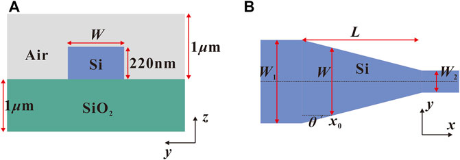
FIGURE 1. Linear waveguide taper: (A) vertical cross section; (B) top view of the linear taper.
Below, we design an adiabatic waveguide taper by the slope-loss algorithm (SLA) first. The proposed AO-SLA uses the above rules to determine the section length of each section. The specific steps are in Section 3.2.
To describe AO-SLA, a well-studied case of an adiabatic taper is used to show in Figure 2, with W1 = 2 µm and W2 = 0.5 µm. A 220 nm-thick silicon planar waveguide (nSi = 3.455) is assumed to be surrounded by silicon dioxide (nSiO2 = 1.445). The wavelength λ0 of light is 1.55 μm. The TE0 mode is chosen for the calculations in this work. The oxide and air thicknesses need to be chosen as a suitable value that can cover the TE0 mode and does not require too much computational time and memory requirements. Under comprehensive consideration, we take the thickness of the air and oxide to be 1 µm. We use the Lumerical Eigenmode Expansion (EME) solver [13] to carry out AO-SLA and SLA.
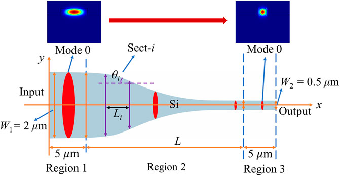
FIGURE 2. Schematics showing the top view of the adiabatic waveguide taper, where the insets show the different fundamental mode shapes at the input and output.
Divide the adiabatic taper into N = 6 sections: (a) Sect-1: W1 = 2 µm to W2 = 1.75 µm, (b) Sect-2: W1 = 1.75 µm to W2 = 1.5 µm, (c) Sect-3: W1 = 1.5 µm to W2 = 1.25 µm, (d) Sect-4: W1 = 1.25 µm to W2 = 1.05 µm, (e) Sect-5: W1 = 1.05 µm to W2 = 0.9 µm, (f) Sect-6: W1 = 0.9 µm to W2 = 0.5 µm. The taper division scheme (such as the numbers of sections and the width variation for each section) were discussed in detail in our previous study [1]. Briefly, the higher the division number NDIV of the SLA/AO-SLA taper, the better the curve of the final structure used for the design, and also the better the results given by the obtained MCTE curve. Nevertheless, the larger the NDIV, the longer the computational time needed. When NDIV is larger than a certain value, the returns to improvement will diminish. In general, NDIV around 10 is enough, and NDIV ∼ 20–30 is perfect, and the obtained MCTE curve will be close to a limiting curve.
Using the SLA, the section length for each section and the final MCTE curve can be obtained, as shown in Table 1; Figure 3, respectively.
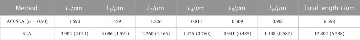
TABLE 1. Comparison of the two algorithms.
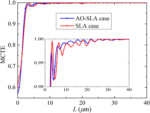
FIGURE 3. MCTE curves for the final adiabatic taper structure designed by using AO-SLA and SLA.
The process for AO-SLA is as follows:
1) Same as that for the SLA case. Other divisions can also be used. For better comparison, the same divisions are used here.
2) Use Eq. 1 to design the adiabatic taper based on the divisions of SLA.
For each section, a linear taper is used to join the input to the output. Taking Sect-i as an example, the initial waveguide width of W1 is joined to the final waveguide width of W2 with a linear taper of length Li, as shown in Figure 4.
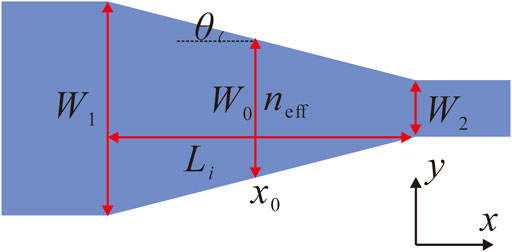
FIGURE 4. Schematics showing the Sect-i of the adiabatic waveguide taper.
According to Figure 4, we can obtain
Substituting Eq. 1 into Eq. 2, we get the following equation:
where W0 = (W1+W2)/2 is the width of the center of the waveguide taper, and neff is the effective index of the cross section at the center of the taper.
[12]claims that α is a constant less than unity, so here we take α = 0.5 first. For α = 0.5, the length of each section obtained is shown in Table 1.
3) Use the length of each section to form the entire adiabatic waveguide taper.
4) Scan the length of the whole adiabatic waveguide taper to get the MCTE curve, as shown in Figure 3.
5) The MCTE curve in step 4 is then applied to obtain the desired length for the adiabatic taper.
As shown in Figure 3, the MCTE curve based on the AO-SLA case has smaller oscillating amplitudes at the top than the SLA case. Hence, the performance of the AO-SLA case is better than the SLA case. They are also compared in Table 1. In Figure 5A, the shapes are shown for the AO-SLA case and the SLA case. Therefore, the difference between AO-SLA and SLA is that for AO-SLA, we use (3) to decide the length of each section for the given MCLF.

FIGURE 5. Comparison of the waveguide shapes for the three cases: (A) the AO-SLA case (green) and the SLA case (blue); (B) the AO-SLA case (green) and parabolic case (red).
The shapes for the parabolic case and the AO-SLA case are also shown in Figure 5B. The MCTE curve obtained for the parabolic case is also plotted in Figure 6. The curve based on the AO-SLA case has smaller oscillating amplitudes at the top than the parabolic curve. Hence, the performance of AO-SLA is better than the parabolic case.
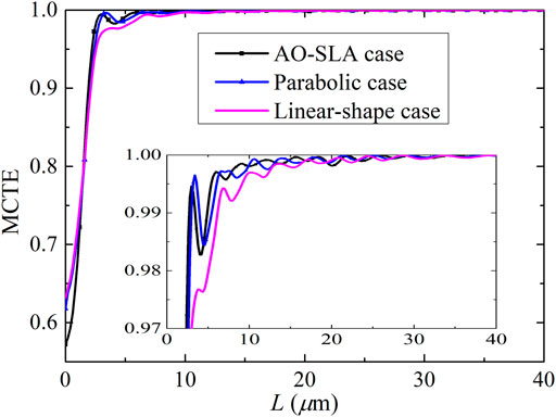
FIGURE 6. MCTE curve for the final adiabatic waveguide taper designed by AO-SLA, where the MCTE curves for the parabolic case and linear-shape case are also shown for comparison.
The MCTE curve obtained for the linear-shape taper is also plotted in Figure 6. The AO-SLA case can give the same power transfer with a much shorter length compared with the linear-shape case. For example, at 98% power transfer, the required lengths are 2.498 μm for the AO-SLA case, 2.782 μm for the SLA case, 2.765 μm for the parabolic case, and 5.048 μm for the linear-shape case. Thus, at 98% power transfer, the required length for the linear-shape case is over 2.02 times longer than the AO-SLA case. Therefore, we have successfully shortened the adiabatic waveguide taper by AO-SLA. This again shows that the design based on AO-SLA is better than those based on the SLA case and parabolic case. Hence, the AO-SLA given is efficient. All calculations in this paper are performed on an Intel(R) Core (TM) i9-10900 2.80 GHz computer with 32 GB RAM.
For the proposed method, it takes approximately 60 s to obtain the length of each section using Eq. 3, plus 300 s to obtain the MCTE curve of the overall structure, which is only about 360 s in total. However, for the SLA algorithm, each section length takes 300 s to obtain. Dividing into six segments took 1800 s, and adding 300 s to obtain the final MCTE curve took a total of 2,100 s using the same computer. Thus, the computational time of the proposed method can be considerably less than that of the SLA method. However, the proposed method can achieve a shorter device length than the SLA method. This is an estimate to give some idea of the design time difference. Therefore, the AO-SLA method is extremely suitable and quite computationally efficient for the design of adiabatic waveguide tapers.
In the design of the adiabatic taper using the AO-SLA, we can choose the constant α according to the application requirements. Table 2 shows the taper length L obtained by AO-SLA with different α for each section.
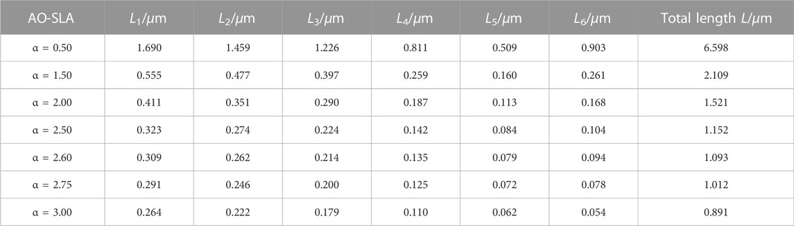
TABLE 2. Comparison of AO-SLA with Different α.
The calculated MCTE curves dependence on the constant α of the adiabatic waveguide taper are shown in Figure 7. From the designed results, we can see AO-SLA with α < 2.5 can achieve better performance. Typically, when α > 2.5, the larger the α is, the larger the oscillating amplitudes are at the top, leading to the worse result. The results here do not agree with the rules derived by [9, 11], and [12]. [11, 12] claimed that α is a constant less than unity [9]. claimed that the adiabatic condition for a taper can be expanded to α ≤ 1.4. However, we believe that the adiabatic condition for the waveguide taper can be expanded to α ≤ 2.5. This is because the proposed AO-SLA is fully numerical, so α can be greater than 1.4. Thus, the proposed AO-SLA is robust and stable (insensitive to change in the adiabatic condition α).
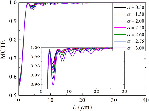
FIGURE 7. MCTE vs L curves for the final adiabatic taper structure designed by AO-SLA with different α.
To show the broad bandwidth of the adiabatic waveguide taper designed by AO-SLA, the output as a function of wavelength is plotted in Figure 8 for the taper designed by AO-SLA (α = 0.5) for the case where the total device length is 12 μm. As shown in Figure 8, the operating bandwidth is defined by no more than 5% loss spans in wavelength from 1,060 nm–2,100 nm, which is an ultra-broad operating bandwidth.
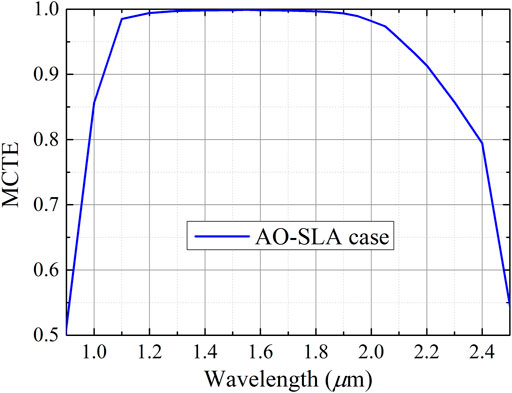
FIGURE 8. Operation bandwidth of the adiabatic waveguide taper for our AO-SLA case with a total structural length of 12 μm.
This work presents a numerical method called AO-SLA for designing compact adiabatic waveguide tapers that are widely applicable to different complex geometries. A waveguide taper is used to introduce the algorithm. We find that the algorithm generates the guided-wave shape that is better than the parabolic taper case and the SLA case. We also show that the adiabatic taper designed by AO-SLA can give a broad operating wavelength bandwidth. Besides, the adiabatic condition α for the adiabatic taper designed by AO-SLA can be extended from α ≤ 1.4 to α ≤ 2.5. Thus, the proposed AO-SLA is efficient, robust, and stable.
The raw data supporting the conclusion of this article will be made available by the authors, without undue reservation.
Conceptualization, T-LL; formal analysis, T-LL and MY; investigation, T-LL and JS; methodology, T-LL and LZ; project administration, XC; writing—original draft, T-LL and XC; writing—review and editing, T-LL and WS. All authors have read and agreed to the published version of the manuscript.
This work was partially supported by the National Natural Science Foundation of China (62161048, 62104117, and 52101017), partially supported by the Natural Science Research Project of Jiangsu Higher Education Institutions (21KJD430001), and partially supported by Nantong Science and Technology Plan Project (JC2020138).
The authors declare that the research was conducted in the absence of any commercial or financial relationships that could be construed as a potential conflict of interest.
All claims expressed in this article are solely those of the authors and do not necessarily represent those of their affiliated organizations, or those of the publisher, the editors and the reviewers. Any product that may be evaluated in this article, or claim that may be made by its manufacturer, is not guaranteed or endorsed by the publisher.
1. Liang TL, Tu Y, Chen X, Huang Y, Bai Q, Zhao Y, et al. A fully numerical method for designing efficient adiabatic mode evolution structures (adiabatic taper, coupler, splitter, mode converter) applicable to complex geometries. J Lightw Technol (2021) 39(17):5531–47. doi:10.1109/jlt.2021.3085306
2. Wu JJ, Shi BR, Kong M. Exponentially tapered multimode interference couplers. Chin Opt Lett (2006) 4(3):167–9.
3. Bogaerts W, Dumon P, Thourhout DV, Baets R. Low-loss, low-cross-talk crossings for silicon-on-insulator nanophotonic waveguides. Opt Lett (28032007) 32(19):2801. doi:10.1364/ol.32.002801
4. Chen CH, Chiu CH. Taper-integrated multimode-interference based waveguide crossing design. IEEE J Quan Electron. (16612010) 46(11):1656–61. doi:10.1109/jqe.2010.2057410
5. Marcatili E. Dielectric tapers with curved axes and no loss. IEEE J Quan Electron. (1985) 21(4):307–14. doi:10.1109/jqe.1985.1072663
6. Weder R. Dielectric three-dimensional electromagnetic tapers with no loss. IEEE J Quan Electron. (1988) 24(5):775775–9. doi:10.1109/3.193
7. Sakai J, Marcatili EAJ. Lossless dielectric tapers with three-dimensional geometry. J Lightwave Technol (1991) 9(3):386–93. doi:10.1109/50.70017
8. Lee CT, Wu ML, Sheu LG, Fan PL, Hsu JM. Design and analysis of completely adiabatic tapered waveguides by conformal mapping. J Lightwave Technol (1997) 15(2):403–10. doi:10.1109/50.554395
9. Fu Y, Ye T, Tang W, Chu T. Efficient adiabatic silicon-on-insulator waveguide taper. Photon Res (2014) 2(3):A41–A44. doi:10.1364/prj.2.000a41
10. Ye T, Fu Y, Qiao T, Chu T. Low-crosstalk Si arrayed waveguide grating with parabolic tapers. Opt Exp (2014) 22(26):31899–906. doi:10.1364/oe.22.031899
11. Burns WK, Milton AF, Lee AB. Optical waveguide parabolic coupling horns. Appl Phys Lett (1977) 30(1):28–30. doi:10.1063/1.89199
12. Milton AF, Burns WK. Mode coupling in optical waveguide horns. IEEE J Quan Electron. (1977) 13(10):828–35. doi:10.1109/jqe.1977.1069240
13.Lumerical Solutions. Mode solutions. Vancouver, Canada: Lumerical Solutions (2018). Available at: https://www.lumerical.com.
Keywords: adiabatic condition, adiabatic taper, integrated optics, optical waveguide design, slope-loss algorithm (SLA)
Citation: Liang T-L, Cheng X, Yu M, Zhang L, Shi J and Shao W (2022) Adiabatic operation slope-loss algorithm for ultrashort and broadband waveguide taper. Front. Phys. 10:1029359. doi: 10.3389/fphy.2022.1029359
Received: 27 August 2022; Accepted: 09 December 2022;
Published: 19 December 2022.
Edited by:
Chuanbo Li, Minzu University of China, ChinaReviewed by:
Ningfeng Bai, Southeast University, ChinaCopyright © 2022 Liang, Cheng, Yu, Zhang, Shi and Shao. This is an open-access article distributed under the terms of the Creative Commons Attribution License (CC BY). The use, distribution or reproduction in other forums is permitted, provided the original author(s) and the copyright owner(s) are credited and that the original publication in this journal is cited, in accordance with accepted academic practice. No use, distribution or reproduction is permitted which does not comply with these terms.
*Correspondence: Tu-Lu Liang, bGlhbmd0dWx1QG50dS5lZHUuY24=; Xi Cheng, Y2hlbmd4aUB4amF1LmVkdS5jbg==
Disclaimer: All claims expressed in this article are solely those of the authors and do not necessarily represent those of their affiliated organizations, or those of the publisher, the editors and the reviewers. Any product that may be evaluated in this article or claim that may be made by its manufacturer is not guaranteed or endorsed by the publisher.
Research integrity at Frontiers
Learn more about the work of our research integrity team to safeguard the quality of each article we publish.