 S. M. Rafi-Ul-Islam
 Zhuo Bin Siu
 Haydar Sahin1,2*
 Mansoor B. A. Jalil
- 1Department of Electrical and Computer Engineering, National University of Singapore, Singapore, Singapore
- 2Institute of High Performance Computing, A*STAR, Singapore, Singapore
We study the quantum valley and Hall conductances in silicene coupled to a ferroelectric (FE) layer. The spin orbit interaction in silicene couples the valley, pseudospin, and real spin degrees of freedom resulting in a topological Berry curvature in the system. The finite Berry curvature in turn induces a transverse Hall conductance. In particular, if the Fermi level Ef is within the bulk energy gap, the Hall conductance is quantized to integer multiples of π. We study the quantum spin and valley Hall conductivities (QSH and QVH) as functions of the applied out-of-plane electric field for different values of Ef and temperature. Both conductivities vary linearly as 1/|Ef| when Ef is within the conduction or valence bands but reach a quantized plateau value when Ef is within the bulk gap. Further, by coupling silicene to a FE layer, the QSH and QVH signals can be modulated by means of the coupling strength. This can potentially provide a robust topological memory read-out with distinct binary outputs over a wide temperature range.
1 Introduction
Silicene is the silicon counterpart of graphene [1–3]. It consists of a monolayer of silicon atoms arranged in a honeycomb lattice with a low-buckled structure that can be described by the Dirac Hamiltonian in pseudospin space [4–6]. Because of its novel electronic properties such as a Dirac cone structure in its low-energy spectrum and the quantum spin and valley Hall effects [7–11], silicene has recently attracted much attention in condensed matter physics, not only for its fundamental scientific significance but also because of its potential applications in semiconductor spintronics [12–17] and valleytronics [18–22].
Compared to graphene, silicene has a much larger spin-orbit coupling strength and a buckled structure. These induce significant coupling between three spin-like degrees of freedom comprising the real, pseudo, and valley spins [11, 23, 24], the interplay of which leads to a rich transport behaviour [25–27]. The strong intrinsic spin-orbit coupling (SOC) in silicene can open a considerable bulk band gap at the Dirac points. Silicene is therefore a good candidate material for investigating the quantum spin Hall state [24, 28]. The coupling of the spin degrees with momentum (k) leads to a finite topological Berry curvature or Chern number [9, 29–31] and therefore, a finite Hall conductivity. This results in a robust topological transport that has been observed in, for example, topological insulators [32–34], skyrmions [35–39], and Weyl/Dirac semimetals [40–45]. In particular, because spin and valley Hall currents can coexist and flow without dissipation in silicene [46–48], it is possible to design devices with low power consumption.
In this work, we show how the quantum valley and spin Hall effects can be obtained and modulated in silicene by exploiting the interplay between the Rashba SOC and coupling to a ferroelectric layer (see Figure 1). We study how the Hall conductivities vary with the out-of-plane electric field, temperature, and Fermi energy. We show that a large band gap opening can be induced in the silicene system by varying the out-of-field electric field Ez to modulate the spin/valley Hall conductivities. Moreover, a sharp step-like change occurs in the valley (spin) Hall conductivities when the magnitude of the out-of-plane electric field exceeds (falls below) the Rashba SOC strength. The QSH, QVH, and quantum phase transitions are manifested by the relative strength of the applied electric field with respect to the SOC strength. This may potentially be utilized in a topological memory device to provide a robust read-out with distinct binary outputs that are insensitive to variations in the temperature and FE texture and other imperfections.
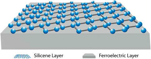
FIGURE 1. Schematic of the system consisting of a silicene layer coupled to a ferroelectric underlayer.
2 Silicene-ferroelectric system
The low-energy Hamiltonian [9, 24] for silicene coupled to a ferroelectric (FE) layer is given by
where the σis refer to pseudospin, and η = ±1 and sz = ±1 are the valley and spin z indices, respectively. Δ is the k-independent effective SOC strength, and lEZ the energy difference between the A and B sublattice sites under substrate effects or an applied out-of-plane electric field Ez [49] caused by the lattice buckling. The Hamiltonian can be written an effective field in pseudospin space as H = σ ⋅b (η, sz) where the effective field is b (η, sz) = (ℏvfkx, − ηyℏvfky, − ηszΔ + lEz). The energy eigenvalues are then given by
where
where
Because η and sz in Eq. 1 can independently take the values of ± 1 and Eq. 1 is a two-by-two matrix, we introduce the collective index n = (λ, η, sz) for convenience to label the eight bands of the system where λ = ±1 denotes whether the band is a valence (λ = 1 with eigenenergy E+) or conduction (λ = −1 with eigenergy E−) band. There are therefore four bands at each of the two valleys.
Here, we treat Δ as a fixed material parameter with the value of 3.9 meV [50] and assume that lEz is a freely adjustable parameter, which can be varied in an experiment by varying the substrate material or applying a gate voltage [49]. It is instructive to examine how the energy distributions of the four bands change with the variation of lEz. As we shall show later, the sign of the Hall conductivity of a completely filled valence band is opposite that of the σz expectation of the states in the band. Eq. 1 therefore implies that the sign of the Hall conductivity of the completely filled valence band is given by that of η(lEz − ηszΔ). Depending on the relative magnitudes of lEz and Δ, the sign of (lEz − ηszΔ) follows that of lEz for the two valence bands corresponding to the two values of ± 1 for sz in each of the two valleys if |lEz| > |Δ|, and has opposite signs in the two valleys for the same value of sz if |lEz| < |Δ|. The change in the relative signs of (lEz − ηszΔ) between the two spin polarizations in a given valley at the critical value of lEz = ±Δ changes whether the Hall conductivities of the four valence bands in the two valleys add up constructively or cancel out in the calculation of the Hall and valley conductivities. Moreover, Eq. 2 implies that the band gap between the conduction and valence bands is 2‖lEz| − |Δ‖, and that the size of the band gap can be changed by modulating the value of Ez. The critical value of lEz = ±Δ at which the band gap vanishes corresponds to a topological phase transition.
The energy dispersion relation is plotted as a function of ℏvfkx in Figure 2. The eigenenergies of the bands in one valley with a given value of sz = ±1 have the same values as those of the corresponding bands in the other valley with the opposite value of sz. As mentioned earlier, when |lEz| < |Δ| (Figure 2A), the two valence band states within the same valley have opposite signs of ⟨σz⟩ (Figure 2A) and when |lEz| > |Δ|, the band gap reopens, but the two valence states in each valley would now have the same sign of ⟨σz⟩ (Figure 2B). The system becomes an insulator if the Fermi energy is located within the gap [8].
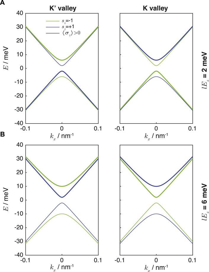
FIGURE 2. K and K′ valley dispersion relations of silicene coupled with a ferroelectric layer with ℏvf = 300 meVnm−1, Δ = 3.9 meV, and (A) lEz = 2 meV, and (B) lEz = 6 meV. The thicker lines indicate the bands with positive values of ⟨σz⟩.
3 Berry curvature and quantum Hall conductivity
The coupling of the silicene monolayer to the FE layer breaks the time-reversal symmetry of the system (as evident from the lEzσz term in Eq. 1, which flips sign under time reversal), and results in a finite Berry curvature Ωn(k), which is defined as
For a two-by-two Hamiltonian with the form of H = b ⋅σ, Ωn can be calculated using
and is explicitly given by
which, as mentioned earlier, is proportional to λ⟨k; λ, η, sz|σz|k; λ, η, sz⟩. Sundaram et al. [51] showed that when an electric field is applied in the x direction, the Berry curvature gives rise to an anomalous velocity in the y direction perpendicular to the applied electric field
where f(E) is the Fermi-Dirac distribution f(E) = 1/(1 + exp ((E − Ef)/kBT)), and
We then define the spin and valley Hall conductivities
For convenience, we define
We first consider the scenario where Ef = 0, i.e., the Fermi level lies within the bulk band gap. In this case,
We have
Here, we note from Eq. 1 that sgn (lEz − szΔη) = − sgn ⟨σz⟩ for a valence band, as mentioned earlier.
We thus obtain
One consequence of Eq. 16 is that when |Δ| > |lEz| in the quantum spin Hall effect (QSHE) regime, the Berry curvatures for the spin up states (sz = 1) in the two valleys have the same sign, and this is opposite to that of their respective spin down (sz = −1) states. This results in the spin up and spin down states being driven along opposite directions perpendicular to the applied electric field by their anomalous velocity [52], giving rise to a spin Hall current (Eq. 17). In contrast, when |Δ| < |Ez| in the quantum valley Hall effect (QVHE) regime, the states in the two spin polarizations in each of the two valleys are driven along the same direction opposite that of the other valley, giving rise to a valley Hall current (Eq. 18). Experimentally, the spin and valley Hall currents may be detectable using electrical means with Hall bar geometries, which has been achieved for superlattices of the related two-dimensional material graphene [53, 54]. Special precautions may need to be taken to protect the silicene sample from exposure to air in the experiment [55]. The results of Eqs. 17, 18 at Ef = 0 meV are summarized in the lEz − Δ phase diagram in Figure 3.
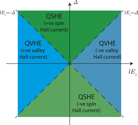
FIGURE 3. lEz − Δ phase diagram at Ef = 0.
We next consider a finite value of the Fermi energy. In an experiment, the Fermi energy can be set through applying gate voltages [55, 56] or by doping [57, 58]. Owing to the anti-symmetries of the Berry curvature about E = 0 as a result of the factor of λ in Eq. 7 and the relation f (E − Ef) = 1 − f (Ef − E) obeyed by the Fermi-Dirac distribution (Figure 4), the Hall conductivities at E = ±Ef are equal to each other. Using this equality and evaluating Eq. 8 for a finite EF at zero temperature, we have
regardless of whether Ef is positive or negative. Note that this expression is consistent with Eq. 16 because |Ef| = |lEz − szΔη| at the minimum of the (λ = +1, η, sz) band and the maximum of the (λ = −1, η, sz) band. The corresponding spin and valley conductivities when Ef is positive and lies above the minima of all the λ = +1 bands, or when Ef is negative and lies below the band maxima of all the λ = −1 bands, is then given by
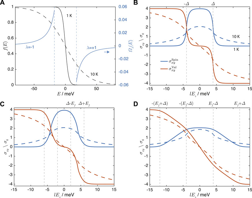
FIGURE 4. (A) The Fermi-Dirac distribution f(E) at Ef = 0 meV and T = 1 K (solid line) and T = 10 K (dotted line), and a representative Berry curvature profile. (B,C). The spin and valley Hall conductivities at T = 1 K (solid lines) and T = 10 K (dotted lines) at (B). Ef = 0 meV, (C). Ef = 2 meV, and (D). Ef = 8 meV. The values of lEz at which qualitative changes occur in the Hall conductivities as discussed in the text are marked out.
Notice that because |Ef| assumes its minimum value at the band minima or maxima, the spin and valley Hall conductivities assume their largest values when Ef is located within the band gap. This is because when Ef lies within the band gap, the valence band will be completely filled and thus all the valence band states will contribute. Because all of these contributions have the same sign, they sum up cumulatively. However, when Ef increases above the band minima of the conduction bands, there will be contributions from some of the conduction band states, which lie below Ef. These contributions have opposite signs from those of the valence bands and thus cancel the contributions from those valence band states, resulting in a lowering of the spin and valley condutivities.
We now investigate the effects of a finite temperature. Figures 4B,C show the spin and valley Hall conductivities at 1 K and 10 K at Ef = 0 meV and Ef = 8 meV, respectively. At the lower temperature of 1 K, the Fermi-Dirac distribution does not deviate very much from the step function profile at 0 K. The step-like switchover between the quantum valley Hall and qunatum spin Hall regimes at lEz = ±Δ with the variation of lEz at Ef = 0 meV implied by Eqs. 17, 18, and Figure 3 is evident in the 1 K curves in Figure 4B. The changes in the Hall conductivities are slightly rounded at lEz = ±Δ because of the finite slope of the Fermi-Dirac distribution with respect to Ef at a finite temperature. In comparison, the variation of the Hall conductivities with lEz are smoother at 10 K because of the larger thermal broadening. In addition, the magnitudes of the peak Hall conductivities tends to be smaller because some of the valence band states near the band maxima are unoccupied and do not contribute, while some of the conduction band states near the band minima are occupied, and contribute with an opposite sign.
We next consider the case where Ef has a finite positive value of 2 meV (Figure 4C), which is smaller than Δ. In contrast to the Ef = 0 meV scenario considered above where the Fermi energy is always within the bulk gap between the conduction and valence bands except at lEz = ±Δ, the location of Ef relative to the band minima and maxima of the conduction and valence bands now varies with lEz because the band gap is dependent on lEz. When Ef has a finite positive value that is smaller than |Δ|, Ef lies in between the band minima of the two conduction bands in each valley when ‖Δ| − |Ef‖ < lEz < ‖Δ| + |Ef‖, and within the bulk band otherwise. When Ef lies between the band minima of the two conduction bands, the spin and valley Hall conductivities both show a linear variation with lEz as shown in the lEz values between Δ ± Ef in Figure 4C. This is because from Eq. 13 with k = kF for the occupied bands and k = 0 for the unoccupied ones, the net spin and valley Hall conductivities is a sum of terms that are linear in both Δ and lEz. The size of this linear region increases with |Ef|. When |lEz| falls outside this range of values, the Fermi energy is located within the bulk band gap, and the qualitative behavior of the spin and valley currents are similar to those of the Ef = 0 case considered in Figure 4B where the system is in the quantum spin Hall regime for |lEz| < |Δ − |Ef‖ and the quantum valley Hall regime for |lEz| > |Δ + |Ef‖. Similarly, at a higher temperature, there is a smoother variation of the Hall conductivities with lEz.
Finally, we consider the case where Ef has a finite positive value of 8 meV (Figure 4D), which is larger than the positive value of Δ considered here. Unlike the |Ef| < |Δ| case considered in the previous paragraph in which Ef is always below the band minima of at least one of the conduction bands, Ef can now lie above the band minima of both conduction bands when |lEz| < Ef − Δ. The independence of the spin Hall conductivity with respect to lEz in Eq. 20 and the linear variation of the valley Hall conductivity with respect to lEz in Eq. 21 in this range of lEz are evident from the 1 K curves. (Note the noticeably smaller magnitude of the spin Hall conductivity and more obvious slope of the valley Hall conductivity in Figure 4D compared to those in Figure 4C in the small |lEz| region. The small slope of the valley Hall conductivity in Figure 4C in the small |lEz| region is due to thermal broadening.) When Ef − Δ < |lEz| < Ef + Δ, the Fermi energy lies between the band minimum of the two bands and both the spin and valley Hall conductivities show a linear variation with lEz. When |lEz| > Ef + Δ, the Fermi energy lies below the minima of both conduction bands in both valleys, i.e., within the band gap. In this case, because |lEz| is also larger than Δ, the system is in the quantum valley Hall regime in which the valley Hall conductivity approaches the constant value of ± 4σ0 and the spin Hall conductivity approaches the constant value of 0. Similar to the Ef = 0 case considered just now, a higher temperature results in a smoother variation of the Hall conductivities with lEz and smaller peak values of the Hall conductivities.
4 Conclusion
In this work, we study the quantum spin Hall (QSH) and quantum valley Hall (QVH) conductivities in a silicene-ferroelectric coupled system, and analyzed the effects of the ferroelectric coupling strength (which in turn affects the energy band gap), temperature, and Fermi energy on these conductivities. Our results show that the QSH and QVH conductivities in the silicene-ferroelectric system can be readily controlled by tuning the electric field arising from the ferroelectric coupling. The coupling could be utilized to ensure a large gap opening (which is proportional to 2‖Δ| − |lEz‖), which would make it easier in practice to align the Fermi energy within the band gap. When this alignment is achieved, the quantum Hall conductivities would attain their maximum quantized values. Additionally, the ferroelectric coupling can be modulated to make the electric field strength equal to the SOC coupling Δ, at which point the QSH and QVH conductivity values exhibit sharp step-like jumps. These sharp transitions between quantized plateau values would be useful for memory applications where either Hall conductivity can serve as a read-out for the binary states of the stored data [59, 60]. Lastly, the QSH and QVH outputs are linked to a topological invariant, i.e., the Berry phase of the system, which confers protection against imperfections and perturbations and robustness against thermal broadening. Hence, utilizing the QSH and QVH effects in the silicene-ferroelectric coupled system as memory outputs would open a new avenue for topological spintronic and valleytronic devices that can be modulated by electrical means.
Data availability statement
The original contributions presented in the study are included in the article/Supplementary Material; further inquiries can be directed to the corresponding authors.
Author contributions
SR-U-I, ZBS, HS, and MJ initiated the primary idea. SR-U-I, ZBS, and HS contributed to formulate the analytical model, to develop codes, to analyze the data and to writing the manuscript under the kind supervision of MJ.
Funding
This work is supported by the Ministry of Education (MOE) Tier-II grant MOE-T2EP50121-0014 (NUS Grant Nos. A-8000086-01-00), and MOE Tier-I FRC grant (NUS Grant No. A-8000195-01-00).
Conflict of interest
The authors declare that the research was conducted in the absence of any commercial or financial relationships that could be construed as a potential conflict of interest.
Publisher’s note
All claims expressed in this article are solely those of the authors and do not necessarily represent those of their affiliated organizations, or those of the publisher, the editors and the reviewers. Any product that may be evaluated in this article, or claim that may be made by its manufacturer, is not guaranteed or endorsed by the publisher.
References
2. Rao C, Biswas K, Subrahmanyam K, Govindaraj A. Graphene, the new nanocarbon. J Mater Chem (2009) 19:2457. doi:10.1039/b815239j
3. Grigorenko AN, Polini M, Novoselov K. Graphene plasmonics. Nat Photon (2012) 6:749–58. doi:10.1038/nphoton.2012.262
4. Brey L, Fertig H. Edge states and the quantized Hall effect in graphene. Phys Rev B (2006) 73:195408. doi:10.1103/physrevb.73.195408
5. Ziegler K. Robust transport properties in graphene. Phys Rev Lett (2006) 97:266802. doi:10.1103/physrevlett.97.266802
6. Rafi-Ul-Islam SM, Siu ZB, Sun C, Jalil MBA. Strain-controlled current switching in weyl semimetals, Phys Rev Appl (2020) 14 (3), 034007. doi:10.1103/PhysRevApplied.14.034007
7. Tabert CJ, Nicol EJ. Optical conductivity of twisted bilayer graphene. Phys Rev B (2013) 87:121402. doi:10.1103/physrevb.87.121402
8. Tahir M, Manchon A, Sabeeh K, Schwingenschlögl U. Quantum spin/valley Hall effect and topological insulator phase transitions in silicene. Appl Phys Lett (2013) 102:162412. doi:10.1063/1.4803084
9. Pan H, Li Z, Liu C-C, Zhu G, Qiao Z, Yao Y. Valley-Polarized quantum anomalous Hall effect in silicene. Phys Rev Lett (2014) 112:106802. doi:10.1103/physrevlett.112.106802
10. Kim Y, Choi K, Ihm J, Jin H. Topological domain walls and quantum valley Hall effects in silicene. Phys Rev B (2014) 89:085429. doi:10.1103/physrevb.89.085429
11. Ezawa M. Valley-Polarized metals and quantum anomalous Hall effect in silicene. Phys Rev Lett (2012) 109:055502. doi:10.1103/physrevlett.109.055502
12. Žutić I, Fabian J, Sarma SD. Spintronics: Fundamentals and applications. Rev Mod Phys (2004) 76:323–410. doi:10.1103/revmodphys.76.323
13. Sun C, Deng J, Rafi-Ul-Islam S, Liang G, Yang H, Jalil MBA. Field-free switching of perpendicular magnetization through spin hall and anomalous hall effects in ferromagnet-heavy-metal-ferromagnet structures Phys Rev Appl (2019) 12 (3), 034022. doi:10.1103/PhysRevApplied.12.034022
14. Tan SG, Jalil MB. Introduction to the physics of nanoelectronics. Amsterdam, Netherlands: Elsevier (2012).
15. Bader S, Parkin S. Spintronics. Annu Rev Condens Matter Phys (2010) 1:71–88. doi:10.1146/annurev-conmatphys-070909-104123
16. Sun C, Rafi-Ul-Islam S, Yang H, Jalil MB. Spin Nernst and anomalous Nernst effects and their signature outputs in ferromagnet/nonmagnet heterostructures. Phys Rev B (2020) 102:214419. doi:10.1103/physrevb.102.214419
17. Fabian J, Matos-Abiague A, Ertler C, Stano P, Zutic I. (2007). Semiconductor spintronics, ArXiv preprint ArXiv:0711.1461. doi:10.48550/arXiv.0711.1461
18. Schaibley JR, Yu H, Clark G, Rivera P, Ross JS, Seyler KL, et al. Valleytronics in 2D materials. Nat Rev Mater (2016) 1:16055. doi:10.1038/natrevmats.2016.55
19. Siu ZB, Jalil M. Effective Hamiltonian for silicene under arbitrary strain from multi-orbital basis. Sci Rep (2021) 11:7575. doi:10.1038/s41598-021-86947-z
20. Zhong D, Seyler KL, Linpeng X, Cheng R, Sivadas N, Huang B, et al. Van der Waals engineering of ferromagnetic semiconductor heterostructures for spin and valleytronics. Sci Adv (2017) 3:e1603113. doi:10.1126/sciadv.1603113
21. Li Y, Zhu H, Wang G, Peng Y, Xu J, Qian Z, et al. Strain-controlled valley and spin separation in silicene heterojunctions. Phys Rev B (2018) 97:085427. doi:10.1103/physrevb.97.085427
22. Vitale SA, Nezich D, Varghese JO, Kim P, Gedik N, Jarillo-Herrero P, et al. Valleytronics: Opportunities, challenges, and paths forward. Small (2018) 14:1801483. doi:10.1002/smll.201801483
23. Tahir M, Schwingenschlögl U. Valley polarized quantum Hall effect and topological insulator phase transitions in silicene. Sci Rep (2013) 3:1075. doi:10.1038/srep01075
24. Ezawa M. Quantum Hall effects in silicene. J Phys Soc Jpn (2012) 81:064705. doi:10.1143/jpsj.81.064705
25. Niu ZP, Zhang YM, Dong S. Enhanced valley-resolved thermoelectric transport in a magnetic silicene superlattice. New J Phys (2015) 17:073026. doi:10.1088/1367-2630/17/7/073026
26. Molle A, Grazianetti C, Tao L, Taneja D, Alam MH, Akinwande D. Silicene, silicene derivatives, and their device applications. Chem Soc Rev (2018) 47:6370–87. doi:10.1039/c8cs00338f
27. Vargiamidis V, Vasilopoulos P. Polarized spin and valley transport across ferromagnetic silicene junctions. J Appl Phys (2015) 117:094305. doi:10.1063/1.4913934
28. Do T-N, Gumbs G, Shih P-H, Huang D, Lin M-F. Valley- and spin-dependent quantum Hall states in bilayer silicene. Phys Rev B (2019) 100:155403. doi:10.1103/physrevb.100.155403
29. Fujita T, Jalil M, Tan S, Murakami S. Gauge fields in spintronics. J Appl Phys (2011) 110:121301. doi:10.1063/1.3665219
30. Ezawa M. Symmetry protected topological charge in symmetry broken phase: Spin-Chern, spin-valley-Chern and mirror-Chern numbers. Phys Lett A (2014) 378:1180–4. doi:10.1016/j.physleta.2014.02.014
31. Tan SG, Chen S-H, Ho CS, Huang C-C, Jalil MB, Chang CR, et al. Yang–Mills physics in spintronics. Phys Rep (2020) 882:1–36. doi:10.1016/j.physrep.2020.08.002
32. Culcer D, Hwang E, Stanescu TD, Sarma SD. Two-dimensional surface charge transport in topological insulators. Phys Rev B (2010) 82:155457. doi:10.1103/physrevb.82.155457
33. Culcer D. Transport in three-dimensional topological insulators: Theory and experiment. Physica E: Low-dimensional Syst Nanostructures (2012) 44:860–84. doi:10.1016/j.physe.2011.11.003
34. Sun H-P, Lu H-Z. Quantum transport in topological semimetals under magnetic fields (II). Front Phys (Beijing) (2019) 14:33405. doi:10.1007/s11467-019-0890-7
35. Zhang X-X, Mishchenko AS, De Filippis G, Nagaosa N. Electric transport in three-dimensional skyrmion/monopole crystal. Phys Rev B (2016) 94:174428. doi:10.1103/physrevb.94.174428
36. Jalil M, Tan SG. Robustness of topological Hall effect of nontrivial spin textures. Sci Rep (2014) 4:5123. doi:10.1038/srep05123
37. Kim BS. Skyrmions and Hall transport. J Phys : Condens Matter (2019) 31:383001. doi:10.1088/1361-648x/ab273f
38. Jalil M, Tan S, Siu Z, Gan W, Purnama I, Lew W. Stability of topological charge of magnetic skyrmion configurations. J Magn Magn Mater (2016) 399:155–8. doi:10.1016/j.jmmm.2015.09.064
39. Fook HT, Gan WL, Lew WS. Gateable skyrmion transport via field-induced potential barrier modulation. Sci Rep (2016) 6:21099. doi:10.1038/srep21099
40. Landsteiner K. Anomalous transport of Weyl fermions in Weyl semimetals. Phys Rev B (2014) 89:075124. doi:10.1103/physrevb.89.075124
41. Rafi-Ul-Islam S, Siu ZB, Sun C, Jalil MB. Realization of Weyl semimetal phases in topoelectrical circuits. New J Phys (2020) 22:023025. doi:10.1088/1367-2630/ab6eaf
42. Hosur P, Parameswaran S, Vishwanath A. Erratum: Charge transport in Weyl semimetals [phys. Rev. Lett. 108, 046602 (2012)]. Phys Rev Lett (2012) 108:079901. doi:10.1103/physrevlett.123.079901
43. Yesilyurt C, Tan SG, Liang G, Jalil M. Klein tunneling in Weyl semimetals under the influence of magnetic field. Sci Rep (2016) 6:38862. doi:10.1038/srep38862
44. Rafi-Ul-Islam S, Bin Siu Z, Jalil M. Topoelectrical circuit realization of a Weyl semimetal heterojunction. Commun Phys (2020) 3:72. doi:10.1038/s42005-020-0336-0
45. Rafi-Ul-Islam S, Siu ZB, Jalil MB. Anti-Klein tunneling in topoelectrical Weyl semimetal circuits. Appl Phys Lett (2020) 116:111904. doi:10.1063/1.5140516
46. Zhang H, Wang H, Xiong S, Han H, Volz S, Ni Y. Multiscale modeling of heat dissipation in 2D transistors based on phosphorene and silicene. J Phys Chem C (2018) 122:2641–7. doi:10.1021/acs.jpcc.7b12333
47. Liu B, Baimova JA, Reddy CD, Dmitriev SV, Law WK, Feng XQ, et al. Interface thermal conductance and rectification in hybrid graphene/silicene monolayer. Carbon (2014) 79:236–44. doi:10.1016/j.carbon.2014.07.064
48. Zhai X, Gao W, Cai X, Fan D, Yang Z, Meng L. Spin-valley caloritronics in silicene near room temperature. Phys Rev B (2016) 94:245405. doi:10.1103/physrevb.94.245405
49. Tsai W-F, Huang C-Y, Chang T-R, Lin H, Jeng H-T, Bansil A. Gated silicene as a tunable source of nearly 100% spin-polarized electrons. Nat Commun (2013) 4:1500. doi:10.1038/ncomms2525
50. Liu C-C, Jiang H, Yao Y. Low-energy effective Hamiltonian involving spin-orbit coupling in silicene and two-dimensional germanium and tin. Phys Rev B (2011) 84:195430. doi:10.1103/physrevb.84.195430
51. Sundaram G, Niu Q. Wave-packet dynamics in slowly perturbed crystals: Gradient corrections and Berry-phase effects. Phys Rev B (1999) 59:14915–25. doi:10.1103/physrevb.59.14915
52. Karplus R, Luttinger J. Hall effect in ferromagnetics. Phys Rev (1954) 95:1154–60. doi:10.1103/physrev.95.1154
53. Komatsu K, Morita Y, Watanabe E, Tsuya D, Watanabe K, Taniguchi T, et al. Observation of the quantum valley Hall state in ballistic graphene superlattices. Sci Adv (2018) 4:eaaq0194. doi:10.1126/sciadv.aaq0194
54. Endo K, Komatsu K, Iwasaki T, Watanabe E, Tsuya D, Watanabe K, et al. Topological valley currents in bilayer graphene/hexagonal boron nitride superlattices. Appl Phys Lett (2019) 114:243105. doi:10.1063/1.5094456
55. Tao L, Cinquanta E, Chiappe D, Grazianetti C, Fanciulli M, Dubey M, et al. Silicene field-effect transistors operating at room temperature. Nat Nanotechnol (2015) 10:227–31. doi:10.1038/nnano.2014.325
56. Drummond ND, Zólyomi V, Fal’ko VI. Electrically tunable band gap in silicene. Phys Rev B (2012) 85:075423. doi:10.1103/physrevb.85.075423
57. Cheng YC, Zhu ZY, Schwingenschlögl U. Doped silicene: Evidence of a wide stability range. Europhys Lett (2011) 95:17005. doi:10.1209/0295-5075/95/17005
58. Sadeghi H, Sangtarash S, Lambert CJ. Enhanced thermoelectric efficiency of porous silicene nanoribbons. Sci Rep (2015) 5:9514. doi:10.1038/srep09514
59. Fujita T, Jalil MBA, Tan SG. Topological insulator cell for memory and magnetic sensor applications. Appl Phys Express (2011) 4:094201. doi:10.1143/apex.4.094201
Keywords: Hall conductance, spin Hall effect (SHE), valley Hall effect, topological insulator (TI), spintronics memories and circuits, silicene
Citation: Rafi-Ul-Islam SM, Siu ZB, Sahin H and Jalil MBA (2022) Valley and spin quantum Hall conductance of silicene coupled to a ferroelectric layer. Front. Phys. 10:1021192. doi: 10.3389/fphy.2022.1021192
Received: 17 August 2022; Accepted: 08 November 2022;
Published: 25 November 2022.
Edited by:
Atsufumi Hirohata, University of York, United KingdomReviewed by:
Farhad Sattari, University of Mohaghegh Ardabili, IranYun-Lei Sun, Zhejiang University City College, China
Copyright © 2022 Rafi-Ul-Islam, Siu, Sahin and Jalil. This is an open-access article distributed under the terms of the Creative Commons Attribution License (CC BY). The use, distribution or reproduction in other forums is permitted, provided the original author(s) and the copyright owner(s) are credited and that the original publication in this journal is cited, in accordance with accepted academic practice. No use, distribution or reproduction is permitted which does not comply with these terms.
*Correspondence: S. M. Rafi-Ul-Islam, ZTAwMjE1OTVAdS5udXMuZWR1; Zhuo Bin Siu, ZWxlc2l1ekBudXMuZWR1LnNn; Haydar Sahin, c2FoaW5oYXlkYXJAdS5udXMuZWR1; Mansoor B. A. Jalil, ZWxlbWJhakBudXMuZWR1LnNn