 Heming Hu1,2†
 Qing Fang
95% of researchers rate our articles as excellent or good
Learn more about the work of our research integrity team to safeguard the quality of each article we publish.
Find out more
ORIGINAL RESEARCH article
Front. Phys. , 21 October 2022
Sec. Optics and Photonics
Volume 10 - 2022 | https://doi.org/10.3389/fphy.2022.1017794
This article is part of the Research Topic Recent Developments in Si-based Materials and Devices View all 8 articles
In this paper, we propose a large wavelength bandwidth Mach-Zehnder modulator based on light intensity equalization structure. The modulator is designed into a symmetric structure to increase the optical operating bandwidth. Besides, two auxiliary MZIs are connected to the respective phase shifters of the main modulator to balance the optical intensity in them. Compared with a conventional Mach-Zehnder modulator, this design has a larger optical operating bandwidth over 56.1 nm. Besides, the maximum extinction ratio of this modulator is 26.2dB, which is 12 dB higher than that of a conventional one. The dynamic extinction ratios at speed of 40Gbps are 4.10 dB in the wavelength of 1530nm and 4.02 dB in the wavelength of 1560 nm respectively. The 3 dB electro-optical bandwidth of this modulator under different voltages are almost consistent with the performance of the conventional one. All of these prove that this structural design can effectively increases the performance of Mach-Zehnder modulators.
Silicon based photonics is a rapidly emerging means in the field of high-speed optical communication [1–5]. As the electrical interconnect has the bottleneck for improving the performance of power consumption, working bandwidth and signal latency, optical interconnect based on silicon photonics is taken as a promising solution to this problem [6, 7]. A key component in the silicon photonics is the optical modulator [8, 9]. The silicon-based optical modulator modulates the light field through the free carrier dispersion effect. The change in the real and imaginary parts of the refractive index has been evaluated qualitatively at telecommunication wavelength of 1.55 μm [10]. For silicon optical modulators, they can be divided into Mach-Zehnder modulators (MZM) [11] and micro-ring modulators (MRM) [12] from the optical structure, and divided into carrier injection [13], accumulation [14] and depletion [15] from the doping structure. Among them, Depletion-based MZM has been widely studied due to its fast modulation rates, high process tolerances, and large modulation bandwidths. However, due to the optical absorption effect by carriers, the optical intensity varies with the carrier concentration during high-speed modulation. This will lead to the deviation of the optical intensity in the two arms of MZM, resulting in a high insertion loss and a low extinction radio after these two lights interfere [16]. To overcome this issue, most of the research in the past are mainly on the asymmetric MZM to improve the device’s extinction ratio performance at specific wavelengths. However, this approach greatly reduces the operating wavelength bandwidth of the device, especially when wavelength division multiplexing technology is adopted.
In order to effectively solve this problem, a symmetrical MZM based on light intensity equalization structure is proposed in this paper. The modulator consists of three symmetrical Mach-Zehnder interferometers (MZI). Two auxiliary MZIs are connected to the respective phase shifters of the main modulator to balance the optical intensity in them. Through this method, the extinction ratio can be greatly improved. Simultaneously, the modulator is furtherly designed into a symmetric structure to increase the optical operating bandwidth. Compared with the conventional MZM, this modulator can obtain a wide optical-operating bandwidth. Besides, the maximum extinction ratio of this modulator is 26.2dB, which is 12 dB higher than that of a conventional one. The dynamic extinction ratios at speed of 40Gbps are 4.10dB and 4.02 dB in the wavelength of 1530nm and 1560 nm respectively. The 3 dB electro-optical bandwidth of this modulator under different voltages is almost consistent with the performance of the conventional one. All of these prove that this design can effectively increases the performance of extinction ratio and wavelength bandwidth in a Mach-Zehnder modulator.
Since carrier dispersion and carrier absorption exist at the same time when the phase shifter is under phase modulation, changes in intensity are inevitable for silicon-based MZI devices based on the plasma dispersion effect [17]. This accompanying intensity change will produce different light field attenuation between the two arms, result in a lower extinction ratio at the output of the interferometer when they combine, the extinction ratio is the ratio between the maximum value and the minimum value of the transmittance in the modulator under external signal modulation, which can be described as ER = 10log (Pout/Pin). At the same time, carrier absorption will cause additional absorption loss when the device working. To solve this problem, most MZMs are designed as asymmetric structures to obtain additional intrinsic phase difference [18]. Even though this method can effectively solve the problem of device extinction ratio, this design will seriously reduce the optical operating bandwidth of the device, which affects the actual optical communication needs of the device.
In order to overcome the above two difficulties, we design a large wavelength bandwidth MZM with optical intensity equalization structure. Figure 1A shows the schematic structure of the designed MZM. The structure can be divided into two parts, each part is designed as a symmetric MZI structure for larger optical operating bandwidth. 1st-1 and 1st-2 are connected with these two phase shifters of 2nd to dynamically balance the optical loss in the two phase shifters during modulation, In the above, 1st-1 represents the auxiliary MZI connected to the 2nd up phase shifter, 1st-2 represents the auxiliary MZI connected to the 2nd down phase shifter, and 2nd represents the MZI structure that implements the modulation function.
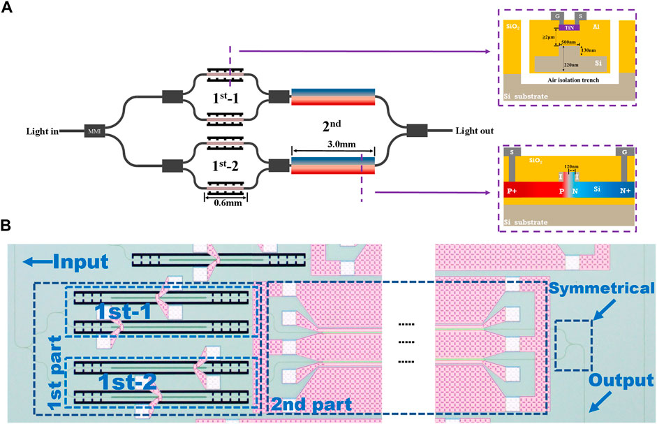
FIGURE 1. (A) The cross section of the light-intensity-balanced MZM. (B) The optical microscope image of the device.
The designed device is fabricated by Singapore AMF. The optical microscope image of the fabricated device is shown in Figure 1B. The device is fabricated on a standard silicon-on-insulator (SOI) wafer mass-produced by Soitec (France), with a top silicon layer thickness of 220 nm and a buried-oxide layer thickness of 2 μm using CMOS compatible processes. The SOI waveguide has a height of 220 nm and a width of 500 nm to meet the single-mode condition of optical signals. To obtain lower device loss, 1st-1 and 1st-2 use the thermo-optic (TO) effect to control the light intensity, while 2nd forms phase shifts through embedded PN junction. For the 1st-1 and 1st-2, due to the significant TO effect in silicon material, the length of 0.6 mm can meet the requirement of optical control. To reduce light absorption loss by the TiN material, we simulated and optimized the distance between the top of the waveguide and the bottom of the TiN heater. As shown in Figure 2, the simulated distance increases gradually, the absorption loss drops sharply. When the distance increases to 1.2 μm, the loss becomes relatively low. Considering the influence of excessively thick oxide layer on the thermal tuning efficiency, the distance between the heater and the top of the waveguide is taken as 1.5 μm. At the same time, in order to reduce the thermal crosstalk while increase the thermal phase shifting efficiency during modulation, deep trench is formed on both sides of the waveguide through deep etching process. For the 2nd, the length of the phase shifter is set as 3 mm to obtain better modulation performance. The N, P doping concentrations for the core of the waveguide are 5e17 cm−3. The heavily N+, P+ doping concentrations are 1e20 cm−3 to ensure the ohmic contact with the metal electrode. Based on previous studies [19], doping compensation method is used in the phase shifter to form intrinsic regions on I region. Through this method, the insertion loss of the device can be greatly reduced while the modulation efficiency can be still maintained at a high level. In this design, the distance between the center of the waveguide and the edge of the two intrinsic regions is 120 nm. The electrical signal is uploaded to the modulator through the traveling wave electrode design.
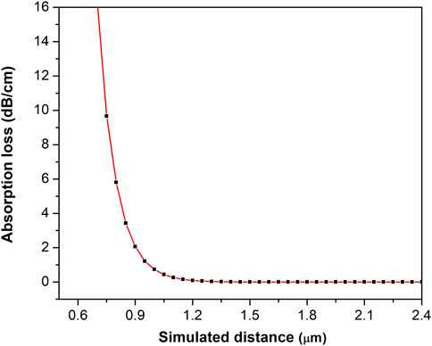
FIGURE 2. Simulated waveguide loss with varying silica thickness.
Before we apply 1st-1 and 1st-2 in the modulator, we first measure the performance of phase shifters in 2nd. The tested phase shift efficiency, transmission loss and VπL of a 3 mm phase shifter is shown in Figures 3A,B. Figure 3A shows the phase shift of the doping compensated waveguide at different voltage. It shows that the optical phase is increased by the effect of the reversed voltage. Particularly, when the applied voltage reaches -8V, the optical signal has the π phase change. Figure 3B shows the measured transmission loss and the VπL of this modulator. Based on this design, the phase shifter has a transmission loss of 3.53 dB at 0 V. As the reverse voltage increases, the width of the depletion layer increases, which leads to a decrease in the transmission loss of the phase shifter. Based on this phenomenon, it can found that when a voltage is applied to one of the 2nd arms, there is a loss difference between them, which leads to a decrease in the extinction ratio performance of the device. Besides, according to the expression
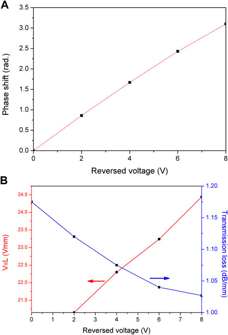
FIGURE 3. (A) The extracted phase shift as a function of the reversed voltage. (B) The transmission loss and VπL as functions of reversed voltage.
After we get the actual performance of the phase shifter in 2nd, we need furtherly characterize the performance of 1st-1 or 1st-2 furtherly. Figure 4 shows the measured transmission spectra of 1st-1. The figure shows the overall transmission of the device from 1520nm to 1620 nm. Since both 1st parts are designed as symmetrical MZI structure, there is only 0.8 dB non-uniform under certain voltage. At the same time, it can be seen from the inset figure that as the applied voltage continues to increase, the transmission loss of the 1st-1 or 2 continues to rise. Compared with the transmission loss at 0V, the transmission loss of the 1st-1 and 1st-2 increases by 1.2 dB at −7 V. Therefore, when the 2nd is under modulation work, a certain loss is applied to the phase shifter through 1st-1 or 2 to ensure that the loss of the two arms is at the same level, result in a high extinction ratio performance of the device.
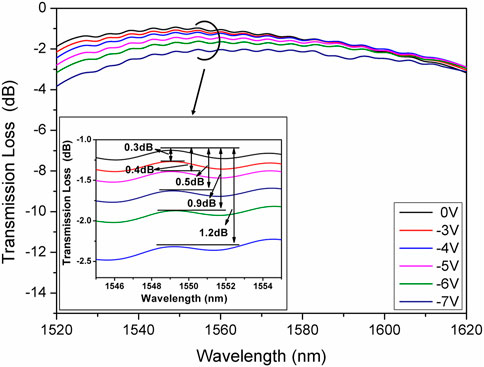
FIGURE 4. Normalized transmission spectra of 1st-1 under various reversed voltages. The inset figure shows the increasing loss at various reversed voltages.
The 1st part should match the dynamic loss of the 2nd during modulation, so we analyze the relationship between the loss difference of the two arms under different modulation voltages in 2nd and the loss that needs to be provided by the 1st part. Figure 5 shows the loss difference between two arms under different voltage. As the applied voltage increases, the loss difference between two arms increases significantly, which will severely reduce the ER of the device. Both arms of the 2nd part are cascaded with a symmetrical MZI structure (1st-1 and 1st-2), 1st-1 and 2 will not affect loss difference of the 2nd part at 0 V. Therefore, only if the voltage is applied to the 1st-1 or 2, it will balance the loss difference of the 2nd part. The loss that 1st part can compensate under different Vbias is also given in Figure 5. When 2nd works under a specific modulation voltage, the voltage required to be applied by the 1st-1 or 2 can be known from this figure.
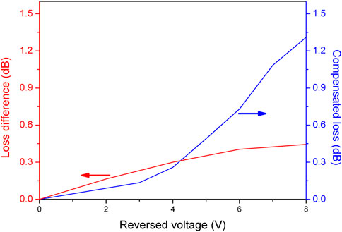
FIGURE 5. The loss difference by two arms of 2nd and the compensated loss offered by 1st-1 and 2 as functions of the reversed voltage.
To prove the performance of this structure improving significantly compared to the conventional asymmetric MZM and symmetric MZM. In this part, a properties performance for both conventional MZI modulators and light-intensity-balanced MZM will be given. The experimental setup is described in much greater detail in Ref. [20]. We tested the spectral transmission of conventional asymmetric MZM, symmetric MZM, and light-intensity-balanced MZM under DC conditions, respectively. The modulation voltage of each MZM is from 0 V to −8 V. In particular, for the MZM with light intensity balanced structure, we achieve the balanced light intensity by applying corresponding voltages to 1st-1 and 2. The specific voltage application conditions are shown in Table 1.
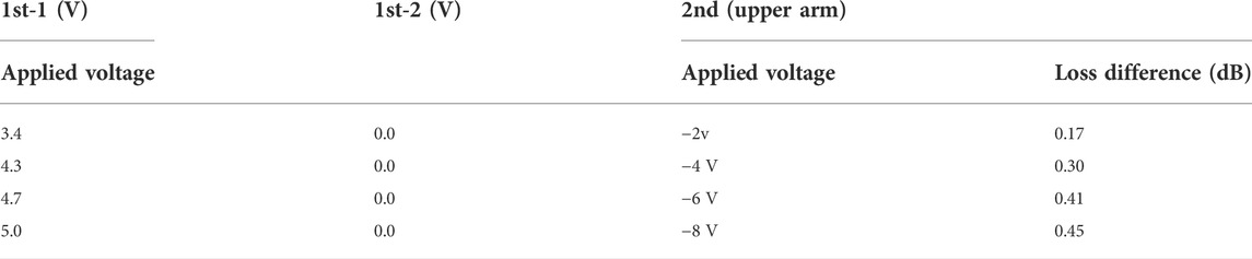
TABLE 1. Applied voltage for 2nd and the required voltages for 1st.
Figures 6A–C shows the measured transmission spectra for asymmetric MZM, symmetric MZM and light-intensity-balanced MZM. For both conventional asymmetric MZM and symmetric MZM, the insertion loss is about 4.9dB, which is mainly caused by the coupling of input and output, the transmission loss of MMI and waveguide. Meanwhile, for the MZM with light intensity balanced structure, the transmission loss of the device is increased by 0.8dB, which comes from the cascade of 1st-1 and 2. However, thermo-optical modulation and short waveguide length are used in 1st-1 and 2, the increase in loss is not obvious. Figure 6A is a transmission spectrum of conventional asymmetric MZM. There is a 1000 μm arm length difference between the upper and lower arms. We can find that the conventional asymmetric modulator can obtain higher extinction ratio at a specific wavelength, but its optical working bandwidth is small. As shown in the inset figure, the optical operating bandwidth of the device is only 0.6 nm under the condition that the extinction ratio beyond 15 dB. For this device, to obtain the extinction ratio performance at a required wavelength, the arm length difference of the device needs to be designed precisely. Figure 6B shows the optical transmission spectrum of a conventional symmetric MZM. Compared with Figure 6A, the device has a great improvement in the optical operating bandwidth due to its symmetric structure. However, for this device, the light intensity imbalance in the two arms caused by the absorption effect of carriers leads to a decrease in the extinction ratio of the device. It can be seen that the maximum static extinction ratio of this device is only 15 dB. Finally, in order to improve the optical operating bandwidth while ensuring the extinction ratio the MZM, we tested the light-intensity-balanced MZM structure. It can be seen from the figure that the structure well solves the problems of conventional asymmetric MZM and symmetric MZM. By matching the voltages in 1st-1 and 2, the device has an extinction ratio beyond 15 dB in the optical operating range of 56.1 nm. The performance comparison of the three structures is shown in Table 2.
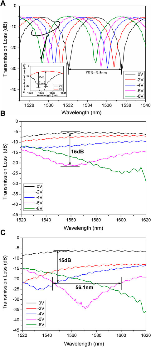
FIGURE 6. The transmission spectrum of (A) conventional asymmetric MZM, (B) conventional symmetric MZM and (C) light-intensity-balanced MZM.
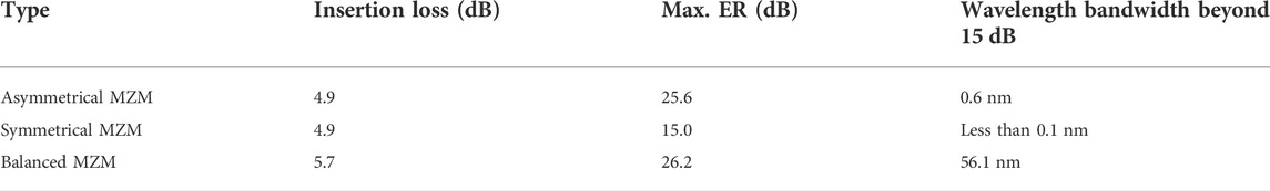
TABLE 2. The performance of the three structures under DC conditions.
Furtherly, the 10Gbps, 20Gbps, 30Gbps and 40Gbps eye diagrams of both symmetric MZM and light-intensity-balanced MZM measured at 1530nm and 1560 nm are shown in Figure 7. As the largest driving voltage swing of 3 V and the standard non-return-to-zero (NRZ) signals in a pseudo-random bit sequence (PRBS) of 232-1 is applied, the eye-diagram extinction ratio of symmetric MZM at different rates is smaller than that of the light-intensity-balanced MZM. Besides, it can be seen from the figure that the extinction ratio of the modulator at 1530nm and 1560 nm has good uniformity. At the modulation rate of 40Gbps, the extinction ratio of the light intensity balanced MZM at the two wavelengths is only 0.08 dB different.
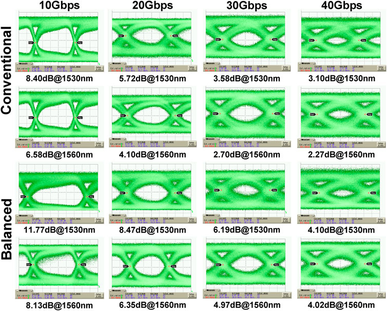
FIGURE 7. The eye diagram for both conventional symmetric MZM and light-intensity-balanced MZM under the speed of 10Gbps, 20Gbps, 30Gbps and 40Gbps for both 1530nm and 1560 nm.
Finally, we tested the S21 parameters of conventional symmetric MZM and light-intensity-balanced MZM. As shown in Figures 8A,B, (A) is the electro-optical bandwidth of the conventional MZM, (B) is the electro-optical bandwidth of the light-intensity-balanced MZM. It can be seen from the figure that the 3 dB bandwidth of the conventional MZM under the bias voltage of 0V, −1V, −2V, −3 V and −4 V is 10.6GHz, 13.7GHz, 14.8GHz, 16.9 GHz and 22.2GHz, while the 3 dB bandwidth of the light-intensity-balanced MZM is 6.6GHz, 12.6GHz, 14.3GHz, 19.1GHz and 20.8Ghz. Compared with the conventional symmetric MZM, the length of the light-intensity-balanced MZM is longer, which leads to a decrease in the device bandwidth to a certain extent. However, since the 1st part does not participate in direct modulation, which makes the bandwidth of the device decreases insignificantly. The light-intensity-balanced MZM can be kept almost at a comparable level with conventional modulators.
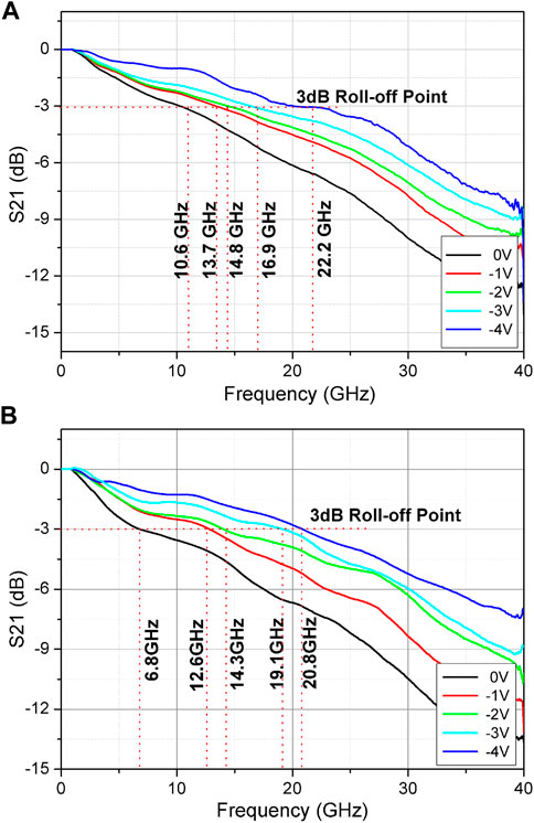
FIGURE 8. (A) The 3 dB bandwidth of conventional symmetric MZM. (B) The 3 dB bandwidth of light-intensity-balanced MZM.
In this paper, we demonstrate a large wavelength bandwidth Mach-Zehnder modulator based on optical intensity equalization structure. With the method of cascaded compensation, the maximum extinction ratio of this modulator is 12 dB higher than that of a conventional one. Compared with the conventional MZI structure, the dynamic extinction ratios at speed of 40Gbps are 4.10 dB in the wavelength of 1530nm and 4.02 dB in the wavelength of 1560nm, respectively, this design has higher modulation performance. At the same time, this structure has little impact on the bandwidth. This modulator provides a solution for future optical communications.
The raw data supporting the conclusions of this article will be made available by the authors, without undue reservation.
All authors listed have made a substantial, direct, and intellectual contribution to the work and approved it for publication.
This work is supported by the National Key Research and Development Program of China (Grant No. 2018YFB2200500), National Natural Science Foundation of China (No. 61764008), Shanghai Municipal Science and Technology Major Project (Grant No. 2017SHZDZX03).
The authors declare that the research was conducted in the absence of any commercial or financial relationships that could be construed as a potential conflict of interest.
All claims expressed in this article are solely those of the authors and do not necessarily represent those of their affiliated organizations, or those of the publisher, the editors and the reviewers. Any product that may be evaluated in this article, or claim that may be made by its manufacturer, is not guaranteed or endorsed by the publisher.
1. Tanaka T, Nishihara M, Takahara T, Yan W, Li L, Tao Z, et al. Experimental demonstration of 448-gbps+ dmt transmission over 30-km smf. In: Proceedings of the 2014 Optical Fiber CommunicationsConference and Exhibition, OFC 2014; March 2014; San Francisco, CA, United states (2014).
2. Wong H, Filip V, Wong CK, Chung PS. Silicon integrated photonics begins to revolutionize. Microelectronics Reliability (2007) 47(1):1–10. doi:10.1016/j.microrel.2006.01.002
3. Jia L, Li C, Liow T-Y, Lo G-Q. Efficient suspended coupler with loss less than -1.4 Db between Si-photonic waveguide and cleaved single mode fiber. J Lightwave Technol (2018) 36(2):239–44. doi:10.1109/JLT.2017.2779863
4. Jia L, Liow TY, Luo X, Tu X, Li C, Yu M, et al. Coherent receiver for dp-qpsk on the soi platform. In: Proceedings of the 21st International Conference on Optical MEMS and Nanophotonics, OMN 2016; July 2016; Singapore, Singapore (2016).
5. Bi X, Li J, Gu Z, Tang B, Sheng C, Yang Y, et al. High sensitivity and dynamic-range 25 gbaud silicon receiver chipset with current-controlled dc adjustment path and cube-shape Ge-on-Si Pd. IEEE Trans Circuits Syst (2020) 67(11):3991–4001. doi:10.1109/TCSI.2020.3011292
6. Siew SY, Li B, Gao F, Zheng HY, Zhang W, Guo P, et al. Review of silicon photonics technology and platform development. J Lightwave Technol (2021) 39(13):4374–89. doi:10.1109/JLT.2021.3066203
7. Sun C, Du L, Zhao J. A brief review of design and simulation methodology in silicon photonics. Tsinghua Sci Technol (2022) 27(3):526–33. doi:10.26599/TST.2021.9010038
8. Liao L, Liu A, Basak J, Nguyen H, Izhaky NJEL, et al. 40 Gbit/S silicon optical modulator for highspeed applications. Electron Lett (2007) 43(22):1196–2. doi:10.1049/el:20072253
9. Feng S, Xue B, Li L, Song L, Zhai X, Zhu C. Waving pin electro-optic modulation structure. Acta Opt (2016) 36(10):1023002. doi:10.3788/AOS201636.1023002
10. Soref RA, Bennett B. Electrooptical effects in silicon. IEEE J Quan Electron (1987) 23(1):123–9. doi:10.1109/jqe.1987.1073206
11. Green WMJ, Rooks MJ, Sekaric L, Vlasov YA. Ultra-compact, low Rf power, 10 Gb/S silicon mach-zehnder modulator. Opt Express (2007) 15(25):17106–13. doi:10.1364/OE.15.017106
12. Dong P, Shafiiha R, Liao S, Liang H, Feng N-N, Feng D, et al. Wavelength-tunable silicon microring modulator. Opt Express (2010) 18(11):10941–6. doi:10.1364/OE.18.010941
13. Tanaka S, Sobu Y. High-speed silicon photonic modulator based on forward-biased pin diodes and passive equalizers. In: Proceedings of the 46th European Conference on Optical Communications, ECOC 2020; December 2020; Brussels, Belgium (2020).
14. Liu A, Jones R, Liao L, Samara-Rubio D, Rubin D, Cohen O, et al. A high-speed silicon optical modulator based on a metal-oxide-semiconductor capacitor. Nature (2004) 427(6975):615–8. doi:10.1038/nature02310
15. Xu H, Li X, Xiao X, Li Z, Yu Y, Yu J. Demonstration and characterization of high-speed silicon depletion-mode mach-zehnder modulators. IEEE J Select Top Quan Electron (2014) 20(4):23–32. doi:10.1109/JSTQE.2013.2293763
16. Hu H, Wang S, Liu Y, Zhang X, Fang QJOC, Gu M, et al. Design of a high extinction ratio silicon optical modulator at 2 µm using the cascaded compensation method. OSA Continuum (2021) 4:1933. doi:10.1364/OSAC.426592
17. Chen X, Wang Z, Chang Y-S, Xu J, Feng J, Yang P, et al. Modeling and analysis of optical modulators based on free-carrier plasma dispersion effect. IEEE Trans Comput -Aided Des Integr Circuits Syst (2020) 39(5):977–90. doi:10.1109/TCAD.2019.2907907
18. Tran TA, Van Yem V, Hantran D, Truong C D. Two mode division (De)Multiplexer based on an mzi asymmetric silicon waveguide. In: Proceedings of the 9th International Conference on Advanced Technologies for Communications, ATC 2016; October 2016; Hanoi, Viet nam (2016).
19. Tu X, Liow T Y, Song J, Luo X, Fang Q, Yu M, et al. 50-Gb/S silicon optical modulator with traveling-wave electrodes. Opt Express (2013) 21(10):12776–82. doi:10.1364/oe.21.012776
Keywords: Mach-Zehnder modulator, SOI platform, large wavelength bandwidth, electro-optical modulator, silicon photonics
Citation: Hu H, Liu S, Ma X, Dong R, Chen H and Fang Q (2022) Large wavelength bandwidth Mach-Zehnder modulator based on optical intensity equalization structure. Front. Phys. 10:1017794. doi: 10.3389/fphy.2022.1017794
Received: 12 August 2022; Accepted: 11 October 2022;
Published: 21 October 2022.
Edited by:
Imran Avci, VU Amsterdam, NetherlandsReviewed by:
Nitesh Mudgal, Poornima College of Engineering, IndiaCopyright © 2022 Hu, Liu, Ma, Dong, Chen and Fang. This is an open-access article distributed under the terms of the Creative Commons Attribution License (CC BY). The use, distribution or reproduction in other forums is permitted, provided the original author(s) and the copyright owner(s) are credited and that the original publication in this journal is cited, in accordance with accepted academic practice. No use, distribution or reproduction is permitted which does not comply with these terms.
*Correspondence: Qing Fang, c2VtaW9lbGFiQGttdXN0LmVkdS5jbg==; Hua Chen, Y2hlcnJ5Y2hlbjQwNjAwQDE2My5jb20=
†These authors have contributed equally to this work and share first authorship
Disclaimer: All claims expressed in this article are solely those of the authors and do not necessarily represent those of their affiliated organizations, or those of the publisher, the editors and the reviewers. Any product that may be evaluated in this article or claim that may be made by its manufacturer is not guaranteed or endorsed by the publisher.
Research integrity at Frontiers
Learn more about the work of our research integrity team to safeguard the quality of each article we publish.