 Yunfeng Hu
 Yangbing Xu
 Jinming Liu2
94% of researchers rate our articles as excellent or good
Learn more about the work of our research integrity team to safeguard the quality of each article we publish.
Find out more
ORIGINAL RESEARCH article
Front. Phys. , 09 September 2022
Sec. Optics and Photonics
Volume 10 - 2022 | https://doi.org/10.3389/fphy.2022.1000909
This article is part of the Research Topic Physical Model and Applications of High-Efficiency Electro-Optical Conversion Devices, volume II View all 11 articles
In large-area dynamic imaging, an active pixel sensor (APS) is proposed. However, there is a trade-off between signal-to-noise ratio (SNR) and spatial resolution. To resolve this, a 256 × 256 active pixel image sensor array based on a 3-D dual-gate photosensitive thin-film transistor (TFT) is presented in this work, with a pixel pitch of 50 μm, pixel fill factor of 63%, photoconductive gain of 102–104 and spatial resolution of 505 ppi. An electronic global shutter is enabled by dual-gate biasing without additional a shutter TFT. Such an array is capable of dynamic imaging at a frame rate of 34 Hz.
Large-area optical image sensor manufactured by thin-film technologies can be found in numerous applications such as flat-panel X-ray detector and optical fingerprint scanning [1–11]. High sensitivity, high spatial resolution, and high speed of response are desirable particularly for dynamic imaging. Conventionally, a pixel consists of a photodetector (PD) and a thin-film transistor (TFT) switch in a passive pixel sensor (PPS) architecture. However, PPS is slow, suffers from low signal to noise ratio (SNR) and is incapable of supporting correlated double sampling (CDS) to remove the noise. To improve the SNR and enable the CDS, an active pixel sensor (APS) with an in-pixel amplifier is designed. APS integrates a PD with multiple TFTs into one pixel. Consequently, it trades high SNR off against high spatial resolution and high fill factor [12–14]. The previous work reported one TFT APS aiming for high SNR, short sampling time, and high fill factor [15]. Even though it results in a decent increase in fill factor as opposed to the 3-TFT APSs, an integration capacitor is still needed to replace a reset TFT [15]. To take an image of a fast-moving object, a CMOS image sensor implements electronic global shutter. As for large-area dynamic imaging, a 4-TFT APS including one additional shutter TFT was proposed in the previous work [16]. However, it inevitably increases the pixel size and reduces the resolution. Despite all aforementioned efforts, the trade-off between SNR, fill factor, and spatial resolution still remains. To resolve the trade-off between SNR and resolution, we have proposed one-TFT APS concept for large area imaging applications [17–20]. This work presents an electronic global-shutter one-Thin-Film-Transistor active pixel sensor array with a pixel pitch of 50 μm and photoconductive gain greater than 100 for large-area dynamic imaging.
The design of the proposed sensor array is depicted in Section 2. The measured results and the performance summary are discussed in Section 3, and finally, we conclude this work in Section 4.
In this work, we report an amorphous silicon (a-Si:H) TFT-based 256 × 256 image sensor array based on electronic-global-shutter one-TFT APS for high-resolution, high-sensitivity, and large-area dynamic imaging applications. Different from improving the spatial resolution by shrinking the TFT size in exchange for a smaller pixel, high resolution in this work is rather achieved by vertically embedding a PD and a switch to form a dual-gate photosensitive TFT.
The schematic pixel structure can be found in Figure 1A. In order to make the TFT photosensitive, a-Si:H channel layer is built in a three-dimensional (3-D) π-shape. Through externally biasing both gates, an internal electric field is created and accordingly separates photo-generated electron-hole pairs and makes the 3-D π-shape channel region become a “virtual” PIN-like PD as seen in the schematic band diagram in Figure 1B. The bottom-gate TFT is therefore PD-gated and its threshold voltage will be light-dependent due to quasi-Fermi level shift upon light exposure as shown in Figure 1B. Figure 1C is the equivalent circuit of the pixel. Such a 3-D dual-gate photosensitive TFT combines a PD, a storage capacitor, and a switch, making pixel fill factor of 63%. High spatial resolution can be attained easily with only one TFT in the pixel. In this work, the image sensor array with 45 μm × 55 μm pixel size and 505 ppi resolution was successfully fabricated in an industrial G2.5 TFT-LCD mass production line.

FIGURE 1. Diagram of pixel. (A) Pixel structure; (B) band diagram; (C) Equivalent circuit.
Figure 2 plots the circuitry diagrams and timing schemes of the proposed one-TFT APS along with the other APS circuits. Similarly, the one-TFT APS presented in this work allows a three-phase pixel operation of reset, integration and readout and the CDS can be enabled by simply applying a reset pulse to the top gate for pixel resetting. The sampling time of the pixel is mainly governed by the resetting operation. Compared with the previous APSs, the proposed one-TFT APS removes the external reset TFT and the external PD as well, thus a reduced pixel sampling time is expected. With a small RC constant, the resetting in this pixel circuit can be done quickly, making it capable of very fast dynamic scanning.
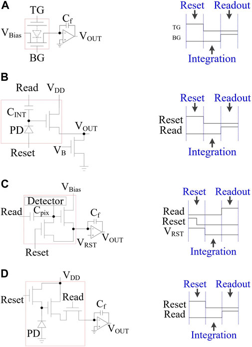
FIGURE 2. Architectures and timing of APS. (A) Proposed 1T APS. (B) 1T1C APS [15]. (C) 2T1C APS [13]. (D) 3T APS [14].
The response speed of dynamic imaging is also dependent on electronic shutter technique. The previous APSs mentioned in Figure 2 use electronic roller shutter to acquire images. In some cases of shooting a fast-moving object, the images would be distorted and/or a ghost image would be presented if the frame rate and/or the sensor were slow.
Figure 3 shows the diagram of sensor array. The array has 256 rows and 256 columns. The top gate lines of the pixels in each column are connected and routed from the top direction, the 256-column top-gated interconnects are named from TG1 to TG256. Similar to the top gate lines, the bottom gate lines of each column are named from BG1 to BG256. The drains of the pixels in each row are connected and routed from the right direction, which are named from VOUT1 to VOUT256. The sources of all pixels are connected to VBias and routed from the left direction. BG1 to BG256 and TG1 to TG256 are used for timing control, VOUT1 to VOUT256 are used for signal output, and VBias is used for voltage bias.
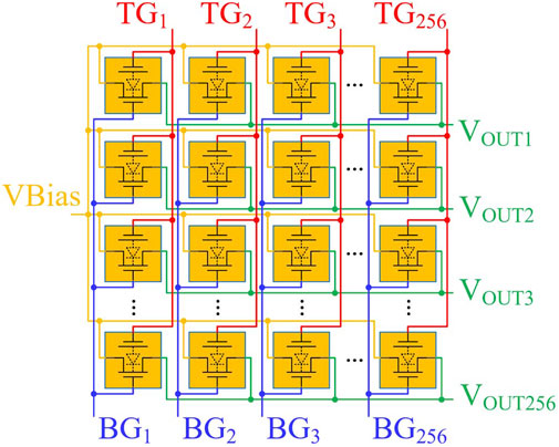
FIGURE 3. Diagram of sensor array.
Figure 4 shows the timing scheme of electronic global shutter in the proposed one-TFT APS. Since the photo-generated charges can be temporarily stored inside the pixel in the integration period through the dual-gate biasing, it is possible to realize electronic global shutter by simply implementing the designed timing scheme in Figure 3 even without a physical shutter TFT. After resetting the whole array, electronic global shutter is initiated by a pulse of light and followed by scanning and reading the array in a sequence.
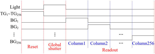
FIGURE 4. Timing diagram of electronic global shutter.
Figure 5 shows the block diagram of image acquisition system where the sensor array is connected by a top-gated driver IC, a bottom-gated driver IC and a 256-channel readout IC (ROIC). The driver ICs are controlled by the FPGA to provide the driving timing, and the ROIC is controlled by the FPGA to collect analog signals and digitize the signals. The FPGA is used to synchronize the timing clocks and assure that the external ICs and the image sensor array work together well during the dynamic image acquisition.
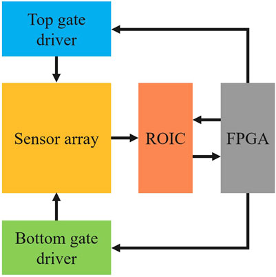
FIGURE 5. Block diagram of image acquisition system.
Figure 6 illustrates device characteristics of the 3-D dual-gate photosensitive TFT. Upon light exposure, the transfer IV curves shift negatively, implying that the threshold voltage drops with light and accordingly the output photocurrent increases as observed in both transfer (Figure 6A) and output characteristics (Figure 6B). Further study unveils that the threshold voltage exhibits a quasi-linear relation with the photon flux (Figure 6C). In pursuing high sensitivity, the proposed one-TFT APS differs from the previous APSs in that the high SNR is achieved by operating the dual-gate photosensitive TFT in the subthreshold region where the output current is an exponential function of the threshold voltage. In another word, a small threshold voltage drop upon light exposure will lead to an exponential increase in the output current. As a result, the proposed photosensitive TFT demonstrates a high photoconductive gain of 102–104, nearly 2–4 orders of magnitude higher than the external quantum efficiency (EQE) of a typical PIN-type PD. It becomes even more important that such a high gain covers an entire studied spectrum with a wavelength ranging from 300 to 1,100 nm. The photosensitive TFT can therefore make a full utilization of all incoming photons in the studied wavelength range and outperform any a-Si:H based PIN-type PDs with an EQE generally below 85% (Figure 6D). Such a high gain can only be found in an avalanche photodiode where a strong electric field must be in presence to trigger avalanche electron multiplication (avalanche effect). However, shot noise also arises under such a strong electric field. Therefore, operating the photosensitive TFT in the subthreshold region becomes a possible approach to achieving high gain while suppressing the noise. Even though operation in the subthreshold region raises a concern of a narrow dynamic range, for low-level light sensing and low-dose dynamic X-ray imaging, high gain and full photon utilization are particularly more important. In the event that does need a wide dynamic range, the dual-gate photosensitive TFT can be tuned to operate in the linear or saturation region where gain is lower but dynamic range becomes wider.
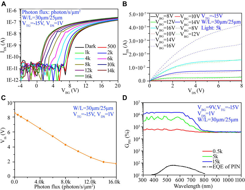
FIGURE 6. Characteristic curve of pixel. (A) Photo transfer characteristics. (B) Output characteristics (dot lines: light; solid lines: dark). (C) Photo-induced threshold voltage (Vth) decrease. (D) Gain (GPH) spectra at various photon fluxes.
Figure 7 shows the micrograph of sensor array and system board where Figure 7A is a micrograph view of the array including pixels and traces and Figure 7B is a system board including driver ICs, ROIC, and FPGA. As shown, the top gates of each column are connected to the top-gated driver ICs, the bottom gates of each column are connected to the bottom-gated driver IC, and the signal outputs of each row are connected to the ROIC. The top-gated driver IC, bottom-gated driver IC and ROIC are all controlled by the FPGA. The image signal is sent to FPGA by ROIC.
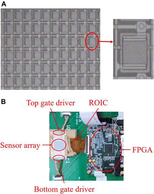
FIGURE 7. Die micrograph and system board. (A) Sensor array. (B) System board.
One example of dynamic imaging using electronic global shutter is shown in Figure 8. Figure 8A is the target image with the characters of “isense” written on the transparent plastic. Figure 8B shows the moving direction of the target image. Figure 8C is a moving record of the target image, and the position of the target image is different at different times. In this example, the frame rate is 34 Hz.
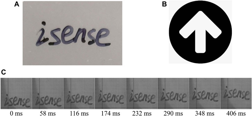
FIGURE 8. Example of dynamic imaging at a frame rate of 34 Hz under light exposure of 11 ms-pulsed green LED. (A) Target image. (B) Moving direction. (C) Sampling frames.
A summary table and comparison with the previous works is given in Table 1. This work adopts a 1T APS structure, which has fewer devices than previous work, so it achieves the following advantages: smaller pixel size (45 μm×55 μm), larger resolution (505 ppi), better fill factor (63%), and higher photoconductive gain (>102). In addition, the array works in global shutter mode, and the frame rate can reach 34 Hz. Moreover, this work can operate in three regions (subthreshold, linear, saturation), while others can only work in two regions (linear, saturation).
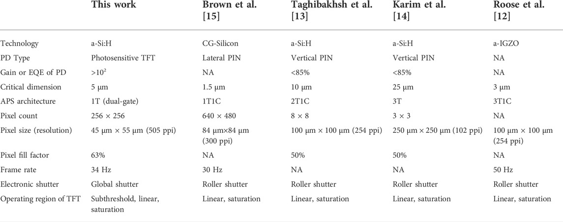
TABLE 1. Comparison table.
In conclusion, we demonstrate a 256 × 256 active pixel image sensor array based on a 3-D dual-gate photosensitive TFT with a pixel pitch of 50 μm, pixel fill factor of 63%, photoconductive gain of 102–104 and spatial resolution of 505 ppi. An electronic global shutter is enabled by dual-gate biasing without additional shutter TFT. Such an array is capable of dynamic imaging at a frame rate of 34 Hz.
The raw data supporting the conclusion of this article will be made available by the authors, without undue reservation.
YH: Designed the image acquisition system, performed the experimental work, and wrote part of the manuscript. YX: Captured the die micrograph of sensor array. JL: Processed image data. YQ: Tested the characteristic curve of pixel. KW: Conceived the project, organized the paper content, wrote, and edited the manuscript.
This work was financially supported by the National Key Research and Development Project of China (Grant No. 2016YFA0202002).
The authors declare that the research was conducted in the absence of any commercial or financial relationships that could be construed as a potential conflict of interest.
All claims expressed in this article are solely those of the authors and do not necessarily represent those of their affiliated organizations, or those of the publisher, the editors and the reviewers. Any product that may be evaluated in this article, or claim that may be made by its manufacturer, is not guaranteed or endorsed by the publisher.
1. Tiao YS, Sheu ML, Wu SM, Yang HM. Ieee. A cmos readout circuit for ltps-tft capacitive fingerprint sensor. In: 2005 IEEE Conference on Electron Devices and Solid-State Circuits; 19-21 December 2005; Hong Kong, China (2005). p. 631–4. doi:10.1109/EDSSC.2005.1635353
2. Xu M, Ou H, Chen J, Wang K. Evaluation of a single-pixel one-transistor active pixel sensor for fingerprint imaging. In: X Zhang, D Erickson, X Fan, and Z Chen, editors. 2015 International Conference on Optical Instruments and Technology: Optical Sensors and Applications; Bellingham. Spie-Int Soc Optical Engineering (2015). doi:10.1117/12.2193336
3. Shin K, KarimA-Si:H KS. a-Si:H TFT-silicon hybrid low-energy X-ray detector. IEEE Trans Electron Devices (2017) 64(4):1624–9. doi:10.1109/TED.2017.2671365
4. Weisfield RL. Amorphous silicon tft X-ray image sensors. In: International Electron Devices Meeting 1998 Technical Digest (Cat No98CH36217); 06-09 December 1998; San Francisco, CA, USA (1998). p. 21–4. doi:10.1109/IEDM.1998.746237
5.CH Lee, I Chan, and A Nathan, editors. Mechanical stress and process integration of direct X-ray detector and tft in a-Si : H Technology. Amorphous and nanocrystalline silicon-based films-2003. Warrendale: Materials Research Society (2003). doi:10.1557/PROC-762-A18.12
6. Sun IK, Sang Wook K, Jae Chul P, Young K, Sang Wook H, Ho Kyung K, et al. Highly sensitive and reliable X-ray detector with Hgi2 photoconductor and oxide drive tft. In: 2011 International Electron Devices Meeting; 05-07 December 2011; Washington, DC, USA (2011). 14.2.1-.2.4. doi:10.1109/IEDM.2011.6131550
7. Liu X, Ou H, Chen J, Deng S, Xu N, Wang K. Highly photosensitive dual-gate a-Si:H tft and array for low-dose flat-panel X-ray imaging. IEEE Photon Technol Lett (2016) 28(18):1952–5. doi:10.1109/LPT.2016.2579199
8. Safavian N, Chaji GR, Nathan A, Rowlands JA. Three-tft image sensor for real-time digital X-ray imaging. Electron Lett (2006) 42(3):150–1. doi:10.1049/el:20063604
9. Huang H, Abbaszadeh S. Recent developments of amorphous selenium-based X-ray detectors: A review. IEEE Sens J (2020) 20(4):1694–704. doi:10.1109/JSEN.2019.2950319
10. Roose FD, Steudel S, Malinowski PE, Myny K, Dehaene W. Active pixel concepts for high-resolution large area imagers. In: International Image Sensor Workshop 2015; June 2015; Vaals. 1. (2015).
11. Jeon S, Ahn S-E, Song I, Kim CJ, Chung UI, Lee E, et al. Gated three-terminal device architecture to eliminate persistent photoconductivity in oxide semiconductor photosensor arrays. Nat Mater (2012) 11(4):301–5. doi:10.1038/nmat3256
12. Roose FD, Myny K, Steudel S, Willigems M, Smout S, Piessens T, et al. 16.5 a flexible thin-film pixel array with a charge-to-current gain of 59µa/pc and 0.33% nonlinearity and a cost effective readout circuit for large-area X-ray imaging. In: 2016 IEEE International Solid-State Circuits Conference (ISSCC); 31 Jan.-4 Feb. 2016; San Francisco, CA, USA. IEEE (2016). p. 296–7. doi:10.1109/ISSCC.2016.7418024
13. Taghibakhsh F, Karim KS. Two-transistor active pixel sensor for high resolution large area digital X-ray imaging. In: 2007 IEEE International Electron Devices Meeting; 10-12 Dec. 2007; Washington, DC, USA. IEEE (2007). p. 1011–4. doi:10.1109/IEDM.2007.4419126
14. Karim KS, Nathan A, Rowlands JA. Amorphous silicon pixel amplifier with/spl delta/V/sub T/compensation for low noise digital fluoroscopy. In: Digest International Electron Devices Meeting; 8-11 Dec. 2002; San Francisco, CA, USA. IEEE (2002). p. 215–8. doi:10.1109/IEDM.2002.1175816
15. Brown C, Hadwen B, Kato H. A 2.6 inch vga lcd with optical input function using a 1-transistor active-pixel sensor. In: 2007 IEEE International Solid-State Circuits Conference Digest of Technical Papers; 11-15 Feb. 2007; San Francisco, CA, USA. IEEE (2007). p. 132–592. doi:10.1109/ISSCC.2007.373623
16. Lai J, Nathan A, Rowlands J. High dynamic range active pixel sensor arrays for digital X-ray imaging using a-Si : H. J Vacuum Sci Technology A: Vacuum Surf Films (2006) 24(3):850–3. doi:10.1116/1.2192526
17. Xu YB, Zhou Q, Huang J, Li WW, Chen J, Wang K. Highly-sensitive indirect-conversion X-ray detector with an embedded photodiode formed by a three-dimensional dual-gate thin-film transistor. J Lightwave Technol (2020) 38(14):3775–80. doi:10.1109/jlt.2020.2977891
18. Wang K, Qi Y, Hu Y, Xu Y, Xu Y, Liu J, et al. Subthreshold operation of photodiode-gated transistors enabling high-gain optical sensing and imaging applications. IEEE J Electron Devices Soc (2020) 8:1236–41. doi:10.1109/JEDS.2020.3022711
19. Wang K, Ou H, Chen J, Nathan A, Deng SZ, Xu NS. 3-D dual-gate photosensitive thin-film transistor architectures based on amorphous silicon. IEEE Trans Electron Devices (2017) 64(12):4952–8. doi:10.1109/ted.2017.2760320
20. Ou H, Wang K, Chen J, Nathan A, Deng SZ, Xu NS, et al. Dual-gate photosensitive fin-tft with high photoconductive gain and near-uv to near-Ir responsivity. In: 2016 IEEE International Electron Devices Meeting (IEDM); 03-07 December 2016; San Francisco, CA, USA. IEEE (2016). doi:10.1109/IEDM.2016.7838529
Keywords: large-area dynamic imaging, electronic global-shutter, one-TFT APS, sensor array, photoconductive gain
Citation: Hu Y, Xu Y, Liu J, Qi Y and Wang K (2022) Electronic global-shutter one-thin-film-transistor active pixel sensor array with a pixel pitch of 50 μm and photoconductive gain greater than 100 for large-area dynamic imaging. Front. Phys. 10:1000909. doi: 10.3389/fphy.2022.1000909
Received: 22 July 2022; Accepted: 22 August 2022;
Published: 09 September 2022.
Edited by:
Qiang Xu, Nanyang Technological University, SingaporeReviewed by:
Zhidong Lin, Wuhan Institute of Technology, ChinaCopyright © 2022 Hu, Xu, Liu, Qi and Wang. This is an open-access article distributed under the terms of the Creative Commons Attribution License (CC BY). The use, distribution or reproduction in other forums is permitted, provided the original author(s) and the copyright owner(s) are credited and that the original publication in this journal is cited, in accordance with accepted academic practice. No use, distribution or reproduction is permitted which does not comply with these terms.
*Correspondence: Kai Wang, d2FuZ2thaTIzQG1haWwuc3lzdS5lZHUuY24=
Disclaimer: All claims expressed in this article are solely those of the authors and do not necessarily represent those of their affiliated organizations, or those of the publisher, the editors and the reviewers. Any product that may be evaluated in this article or claim that may be made by its manufacturer is not guaranteed or endorsed by the publisher.
Research integrity at Frontiers
Learn more about the work of our research integrity team to safeguard the quality of each article we publish.