- 1National & Local Joint Engineering Research Center for Intelligent Manufacturing Technology of Brittle Material Products, Huaqiao University, Xiamen, China
- 2Institute of Manufacturing Engineering, Huaqiao University, Xiamen, China
- 3Fujian Norstel Material Technologies Co., Ltd., Quanzhou, China
Subsurface damage of 4H-silicon carbide (SiC) wafers, which is detrimental to the performance and lifetime of SiC-based photoelectric devices, is easily induced during surface machining process due to their particular mechanical and physical properties. A nondestructive and effective characterization technique is essential for high quality products in the wafer manufacturing process. A method based on the Mueller Matrix Spectroscopic Ellipsometry (MMSE) is proposed to detect the nanoscale subsurface damage of 4H-SiC wafers induced by grinding and polishing. The Mueller matrix elements which are sensitive to the damage information have been identified through both simulation and experiment. The damage layer and its roughness are considered in optical modeling at different processing stages. The results show that both the surface texture and the damage layer contribute to the Mueller matrix values. The fitting thickness of the damage layer is consistent with the value from transmission electron microscope (TEM); the refractive index of the damage layer matches the surface elements analysis result from X-ray photoelectron spectroscopy (XPS). The results suggest that the MMSE-based method could offer a promising nondestructive method to detect global wafer subsurface damage and its evolution during grinding and polishing, which eventually could benefit process optimization in the whole wafer manufacturing process.
1 Introduction
4H-silicon carbide (SiC) is considered as one of the most promising third-generation semiconductor materials with applications in many cutting-edge fields, such as semiconductor electronics, optics, and graphene growth [1, 2]. The state-of-the-art SiC device structures are currently grown on the 4H-SiC off-axis cut wafers, which can stop the propagation of threading defects in epilayers [3]. Comparing to C-face, Si-face is more useful for epitaxial film growth [4]. Conductive SiC (n-type doped) substrates are used for homoepitaxial device structures such as Schottky diodes [2] and MOSFETS [5]. The premise of those applications is the availability of affordable, high quality, large diameter SiC substrates. However, SiC is a typical difficult-to-machine material due to its high hardness and strong chemical inertness. The subsurface damage (SSD) is easily caused during substrate processing [6], which will impair the mechanical, electronic, and optical properties of materials [7]. For this reason, the characterization of subsurface damage is conducive to advanced applications.
The processing flow of SiC substrate mainly includes rough grinding, fine grinding, and chemical mechanical polishing (CMP) [7, 8]. Usually, rough grinding will leave large surface texture and a mass of subsurface damage. Although those damages can be gradually removed by subsequent fine grinding and CMP, it is time-consuming. Therefore, monitoring the depth of damage will provide a useful index for the quality control of SiC wafer production chain and the processing technology optimization, especially for wafers with large diameters, which is a trend with the development of material growth. A nondestructive and precise method for measuring the thickness of the SSD layer is indispensable.
Several destructive and nondestructive methods have been used to detect the SSD [9–11]. The destructive methods, for example, cross-sectional microscopy, taper polishing, chemical etching, magnetorheological finishing (MRF) polishing, the inductivity coupled plasma method [12], and TEM microscopy can measure different damage depths from slicing to CMP. These destructive methods are time-consuming and reduce production efficiency and increase cost. The nondestructive methods include micro-Raman spectroscopy, optical coherent tomography, photoluminescence, and laser scattering method. However, their detection accuracy or efficiency is limited, or inappropriate for accurately measuring the thickness of the very thin damage layer.
As a nondestructive strategy, the Mueller Matrix Spectroscopic Ellipsometry (MMSE) is commonly used to measure the thickness and refractive index of thin films and crystal with excellent accuracy [13, 14]. Previously reported refractive ellipsometric characterizations in SiC wafers have been done [17] but were limited in single-sided polished wafer without backside reflection [15] or treated the damage layer as an SiO2 film [16]. Our group [17] took double-sided polished n-type 6H-SiC wafer with backside reflection and the damage layer into account based on partial-wave coherence theory. However, effectively assessing the damage layer in the rough stage of grinding or polishing was excluded. Meanwhile, the fitting process was complex and time-consuming. Yao et al. [18] proposed a quasi-Brewster angle technology to quickly evaluate the polishing quality covering rough- and fine-polishing stages using a variable angle ellipsometer, but the thickness of the damage layer was not obtainable. Therefore, quantitative and accurate measurement of the damage layer is essential in different processing stages (rough grinding, fine grinding, and CMP). There are three key issues that need to be addressed. First, the optical constants of SiC must be known well [19]. Second, the sensitivity of the Mueller matrix to the damage layer and surface texture needs to be investigated. Third, the ability of MMSE to characterize the damage layer during the process of rough grinding, fine grinding, and CMP needs to be verified.
In this paper, the damage layers induced by rough grinding, fine grinding, and CMP 4H-SiC off-axis cut wafers are characterized by MMSE. The subsurface quality in the wafer processing is visualized. The paper is arranged as follows: In Section 1, the background is introduced. In Section 2, the samples and experimental instruments are presented. In Section 3.1, a method to extract optical constants of uniaxial 4H-SiC crystal is given. In Section 3.2, optical stack models are established according to the damage characteristics. In Section 3.3, the Mueller matrix sensitivity for the damage layer is simulated and verified by experiment. In addition, Mueller matrix sensitivity for the direction of surface texture is investigated. In Section 4, the accurate optical constants of 4H-SiC crystal are illustrated. The thicknesses and refractive indices of damage layers are analyzed and compared with those given by TEM and XPS.
2 Samples and Experimental Instruments
4H-SiC single crystal wafers (n-type doped, off-axis cut toward <1120>, 4 inch) after double-sided rough grinding, double-sided fine grinding, and double-sided CMP were selected for research. The Mueller matrix of wafers was measured in transmission and reflection modes with a dual-rotation compensator Muller matrix ellipsometer (DRMME, Wuhan Eoptics Technology Co., China) [20, 21]. Measurements were done in the spectral range of 250 nm (4.96 eV) to 1400 nm (0.89 eV). The short axis diameter of the incident beam spot is 3 mm.
The Si-face surface morphology of 4H-SiC wafers was measured by Atomic Force Microscope (AFM) (Alpha300 RA, WITec, Germany) and 3D optical surface profiler (Newview 7300, ZYGO, United States). The surface roughness of rough grinding, fine grinding, and CMP 4H-SiC wafers were obtained by 3D optical surface profiler, and they were 13.26 nm, 0.78 nm, and 0.32 nm, respectively.
The measurements of optical Absorbance (A), Transmittance (T), and specular Reflectance (R) were done with a UV-Vis-NIR spectrophotometer (Perkin Elmer, lambda-1050). Absorbance spectra were used to obtain the bandgap of 4H-SiC. Transmittance and reflectance spectra were used to calculate the ordinary extinction coefficient of wafers.
The XPS analysis has been performed using the spectrometer (Thermo Fisher Scientific, K-alpha+) with AlK
3 Ellipsometric Characterization Theory
3.1 Optical Constants of 4H-SiC
Complex optical constants
The optical anisotropy of uniaxial 4H-SiC wafer is obtained by analyzing the transmission Mueller matrix (MM), as shown in Figure 1A. The
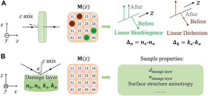
FIGURE 1. (A) The transmission Mueller matrix measurement of off-axis cut uniaxial 4H-SiC wafer. The linear birefringence and linear dichroism can be analyzed. (B) The reflective Mueller matrix measurement of processed 4H-SiC wafer with the damage layer. The refractive index and thickness of the damage layer and the surface structure anisotropy of the rough grinding wafers can be analyzed.
Based on the measured complex retardance
In general, the equation gives the algebraic relation between complex optical anisotropy
Moreover, the ordinary extinction coefficient
where d is the thickness of the wafer along the direction of light propagation. The thickness of the CMP wafer is obtained by digital micrometer with a value of 356.51 ± 0.44
Theoretically, each dielectric tensor is rotated from its standard setting to the measurement coordinate system to obtain the objective results. The laboratory coordinate system is defined in Figure 1, and an orthogonal transformation is given by:
where A
It is hard to ensure the optic axis is completely parallel to the incident plane in the DRMME experiment. Therefore, it is necessary to evaluate the error of the Mueller matrix caused by Euler angles. The formula is defined by:
where
3.2 Optical Stack Model
In MMSE reflection measurement, an appropriate optical stack model is acquired to obtain the accurate parameters of thin layers. The refractive index, thickness of the damage layer and surface structure anisotropy of the wafers can be analyzed, as shown in Figure 1B.
According to the processing mechanism of brittle materials [25], the surface and subsurface damage of SiC wafers corresponding to rough grinding, fine grinding, and CMP are different. Figure 2 shows the AFM images that visible scratches and pits damage left on the rough grinding wafer (Figure 2A), scratches left on the fine grinding wafer (Figure 2B), and those are absent from the CMP wafer (Figure 2C).
Besides that, invisible subsurface damage (SSD) is formed above the pure substrate [26], as shown in Figure 3. The SSD caused by grinding most contains cracks, phase transformation, an amorphous layer, residual stress, and other types of damage. After CMP, the SSD mostly only contains an amorphous layer. We simplified the model because the SSD on the backside of the wafer is basically the same as that on the surface.

FIGURE 3. Schematic diagrams of (A) rough grinding, (B) fine grinding, and (C) CMP surface/subsurface cross-section of 4H-SiC wafers.
From Figure 3A, rough surface, amorphous layer, nonideality boundary (between the damaged zone and pure substrate), and roughed backside are characteristics of the rough grinding wafer surface from top to bottom. These peculiarities are considered for ellipsometric analysis using roughness layer, damage layer, interface layer, and semi-infinite SiC substrate. For fine grinding wafers (Figure 3B), there are surface scratches and nonideality damage layer, which are modeled as three layers: roughness layer/damage layer/SiC substrate. CMP wafer with the sub-nanometer roughness is regarded as a specular surface judged by Rayleigh criterion [27]. Therefore, the roughness is omitted and the CMP wafer (Figure 3C) is modeled as two layers: damage layer/SiC substrate.
For each optical stack model, the optical constants of 4H-SiC are set as known from the calculation in Section 4.1. The interface layer is modeled by the Bruggeman Effective Medium Approximation (B-EMA), which consists of 50% pure substrate and 50% damage layer. The Cauchy dispersion relation is used to model the damage layer given by:
where A and B are fitting Cauchy parameters and λ is the wavelength in micrometers. The roughness layer is modeled by a B-EMA layer formed by 50% bulk material and 50% air.
3.3 The Sensitivity of the Mueller Matrix
Different from the traditional thin film analysis, the sensitivity of ultra-thin damage layer needs to be considered in optical modeling for fine grinding and CMP samples with backside reflection. Besides that, the effect of surface texture caused by rough grinding on the Mueller matrix needs to be considered.
First, to figure out the role of surface (Si-face), back (C-face) damage layer, and the backside reflection in the Mueller matrix, the following simulation is executed in Figure 4A. Using partial coherence wave [28] and fully coherence wave theory, four models are used to explore the response of the Mueller matrix elements to the ultra-thin layer on the Si-face and the C-face of the 4H-SiC substrate. A known SiO2 layer is used as the material of ultra-thin film. Model 1, 350 μm 4H-SiC thick layer with backside reflection. Model 2, 2 nm SiO2 layer on Si-face of 4H-SiC thick layer with backside reflection. Model 3, 2 and 5 nm SiO2 layers on Si-face and C-face of the 4H-SiC thick layer with backside reflection. Model 4, 2 nm SiO2 layers on the Si-face of the 4H-SiC semi-infinite substrate without backside reflection. The angle of incidence is 65° and the Euler angle
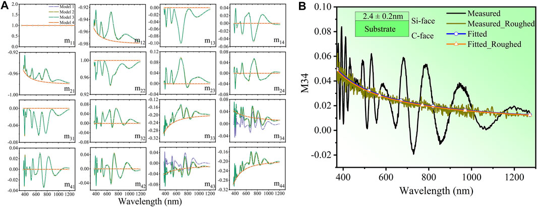
FIGURE 4. The simulation of the Mueller matrix. (A) Model 1, 350 μm 4H-SiC thick layer with backside reflection. Model 2, 2 nm SiO2 layer on the Si-face of the 4H-SiC thick layer with backside reflection. Model 3, 2 and 5 nm SiO2 layers on the Si-face and the C-face of the 4H-SiC thick layer with backside reflection. Model 4, 2 nm SiO2 layers on the Si-face of the 4H-SiC semi-infinite substrate without backside reflection. The angle of incidence is 65° and the Euler angle γ is 45°,
From the simulation results, the diagonal element M34 has the highest sensitivity to small changes of the ultra-thin layer compared to other elements. The difference between Model 1 and Model 2 indicates that M34 is only sensitive to the thin layer. The difference between Model 2 and Model 3 indicates that the thin layer on the C-face of the substrate has almost no effect on the values of the Muller matrix. The difference between Model 2 and Model 4 indicates that the fluctuation of MM spectra is related to the backside reflection of substrate. Moreover, the “position balance” of M34 spectra of substrate with backside reflection is the same with that of substrate without backside reflection. Therefore, we can omit the backside reflection when only considering the fitting result of the M34 element.
Furthermore, the backside of the CMP wafer is roughed for experimental comparison. We simplify the optical model to fit the thickness of the damage layer by applying the fully coherence theory to CMP SiC wafer with and without backside reflection. Figure 4B shows the measured and fitted M34 element of backside polished and roughed wafer. The oscillation in the experimental data of polished ones comes from the backside reflection. Fitting the polished sample using the fully coherence theory is equivalent to using a semi-infinite substrate model and ignoring the effect of the backside reflection. The thickness results of damage layers obtained by fitting the MM data from the same point before and after roughening are 2.4 ± 0.2 nm and 2.5 ± 0.2 nm, respectively. In addition, we obtained the same fitting M34 curve at the same point before and after roughening (Figure 4B). The fitting results further confirm that the backside reflection of the substrate can be ignored when only the thickness of the damage layer is fitted.
Next, to appropriately describe the influence of the surface texture of rough grinding 4H-SiC wafers on the MM spectra, the MM elements are plotted in polar coordinates with wavelength and rotation angle as radial and angular coordinate, respectively. The reflection MM data is measured at 17 Euler rotation angles (
For demonstration, one point of rough grinding wafer is selected. Figure 5A shows the surface morphology measured by a 3D optical surface profiler and its initial texture direction is parallel to the plane of incidence. Figure 5B shows the schematic diagram of reflection ellipsometry measurement. The measured 4
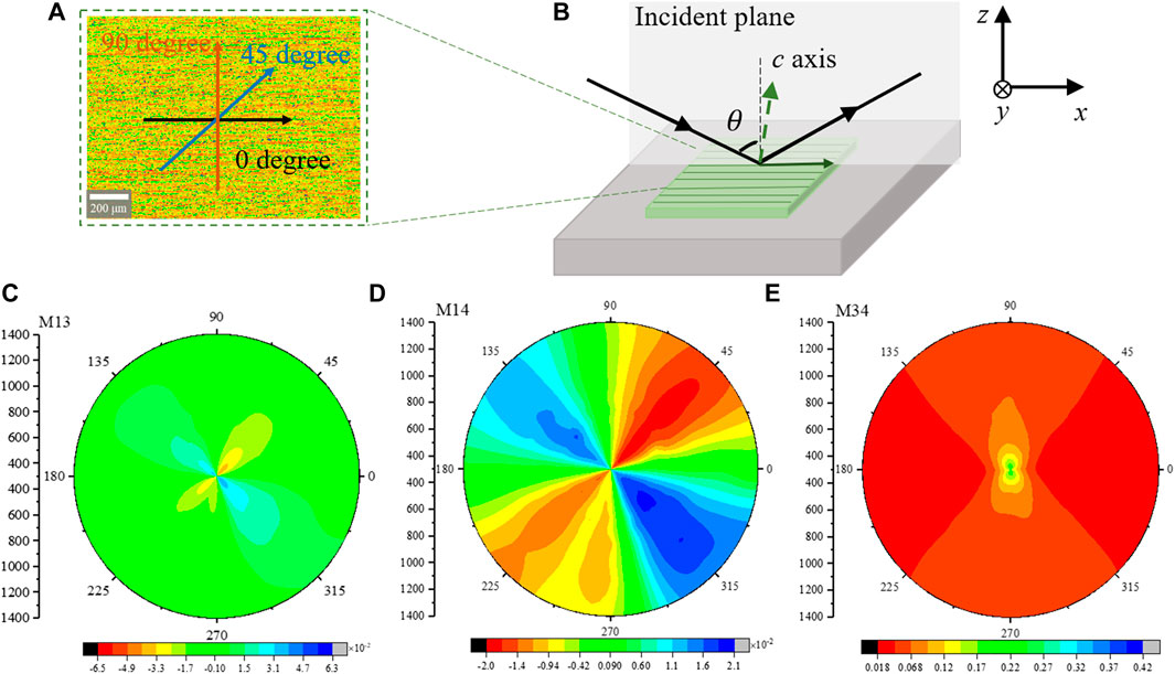
FIGURE 5. (A) The surface morphology of the rough grinding wafer and its initial texture direction parallel to the plane of incidence where the direction of rotation angle is anticlockwise. (B) The schematic diagram of reflection ellipsometry measurement. (C–E) are the experimental MMSE data of individual M13, M14, and M34 elements from 0 to 360° rotation angles in 65° incident angle, respectively. MM intensities are plotted in polar coordinates with wavelength and rotation angle as radial and angular coordinate.
The measurement data indicate that the off-diagonal elements depend on rotation angles and the Mueller matrix has a high sensitivity to structure anisotropy. It can be observed that the off-diagonal elements are zero at 0°, 90°, 180°, and 270° rotation angles. The maximum and minimum values of M13 and M14 spectra are located at 135°, 315° and 45°, 225° rotation angles, respectively. Therefore, off-diagonal Mueller matrix elements can be set as an indicator to judge the direction of the surface rough texture [29]. The result of diagonal element M34 shows that the maximum and minimum values are located at rotation angles of 90° and 0°, respectively. It indicates that when the texture direction of roughness is perpendicular to the incident plane, there are more prominent responses from the Mueller matrix. In this view, the roughness does not appear as an intrinsic characteristic of the surface, which depends on the wavelength and on the direction of propagation of the incident wave.
4 Results and Analysis
4.1 Transmission Spectra Analysis
The bandgap of 4H-SiC calculated by Tauc-plot is about 3.3 eV, as shown in Figure 6A. Figure 6B shows the R and T spectra of 4H-SiC CMP wafer in wavelength range from 220 to 2000 nm. Ordinary extinction coefficient (ko) is first calculated using Equation 5, as shown in Figure 6F. Then, combined with Mueller matrix differential calculus, the linear birefringence
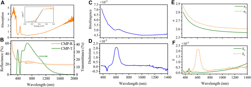
FIGURE 6. Transmission measurement of CMP 4H-SiC wafer with off-axis cut angle. (A) Absorption spectra and Tauc-plot, the bandgap 3.3 eV is calculated. (B) Reflectance and transmittance spectra. (C) Birefringence. (D) Dichroism. (E) Refractive indices (no and ne) and (F) extinction coefficients (ko and ke) of 4H-SiC crystal.
4.2 Reflection Mueller Matrix Analysis
Figures 7A–C show the schematic diagrams of multilayer optical models corresponding to the cross-section characteristics of 4H-SiC wafers after three machining stages. From the simulation results in Section 3.3, the fully coherence wave theory can be used on wafers with and without back reflection, and the value of M34 element can be used as an indicator of the damage layer. Therefore, only the fitted M34 elements are compared with the experimental data of three processed wafers, as shown in Figures 7D–F. The smooth curve of measured M34 in Figure 7D indicates backside reflection is absent from the rough grinding wafer. The fluctuating curves of measured M34 in Figures 7E,F are affected by backside reflection, and their amplitude is related to the absorption of samples. The fluctuations decrease in three higher extinction coefficient ranges, corresponding to 430–480 nm (ke), 520–650 nm (ke), and 1100 nm–1400 nm (ko and ke) (Figure 6F).
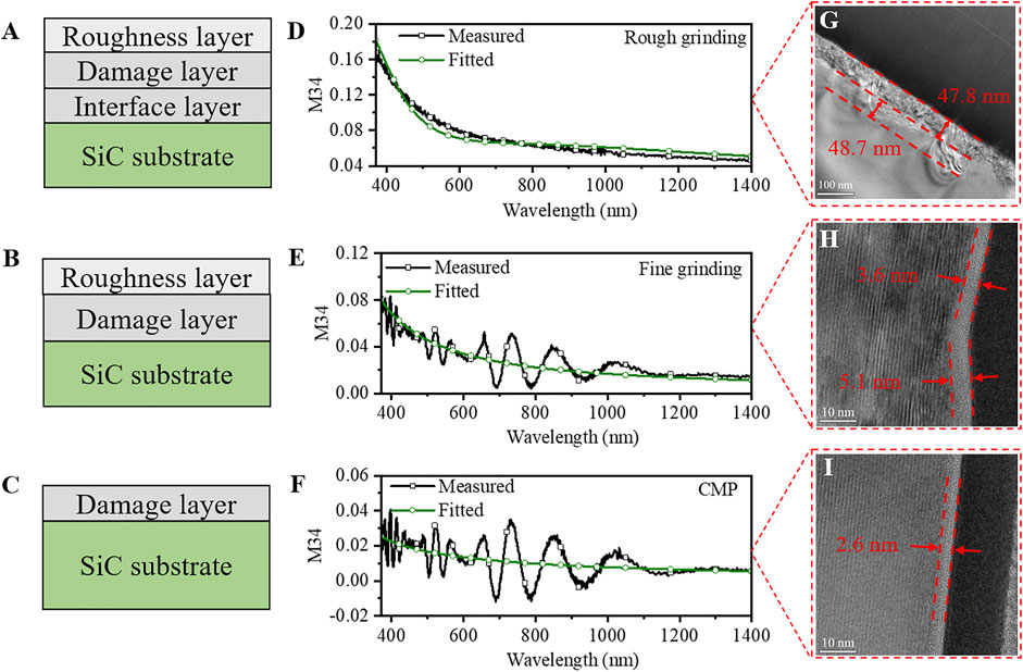
FIGURE 7. (A–C) are the schematic diagrams of optical stack models. (D–F) are fitting results of M34. (G–I) are the typical TEM images of rough grinding, fine grinding, and CMP 4H-SiC wafers.
The thicknesses of the roughness layer of rough grinding and fine grinding wafers are initialed by 3D optical surface profiler results, while no roughness layer is set for the CMP wafer. Based on the prior knowledge [17], the Cauchy parameters of the damage layer are initialed as follows: A is 2, B is 0.05 μm2, and the initial thicknesses of damage layers are set to 50 nm, 4 and 2 nm for rough grinding, fine grinding, and CMP wafers according to their processing techniques, respectively.
By fitting the MMSE data, the damage layer thicknesses of rough grinding, fine grinding, and CMP wafers are obtained as 53.7
The rough grinding also left an interface inhomogeneity (about 48.7 nm thick in one position) under the damage layer, as shown in Figure 7G. The average thickness is about 53.7
Moreover, the refractive indices of the damage layers after three machining stages are compared with that of 4H-SiC crystal, as shown in Figure 8. The refractive indices of all damage layers are smaller than those of the SiC crystal, which means the destruction of the silicon carbide structure and the introduction of other atoms, such as oxygen. The higher refractive index of the rough grinding wafer than those of the fine grinding and CMP wafers can be explained by incomplete amorphization of the damaged zone (Figure 7). The higher refractive index of the CMP wafer than that of the fine grinding wafer can be explained by different atomic ratios of elements in XPS analysis (Section 4.3).
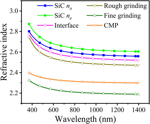
FIGURE 8. The refractive index of the damage layer of three processed wafers compared with that of 4H-SiC crystal.
In general, with further processing, the thickness of the damage layer gradually decreases and the quality of the wafer after CMP has been significantly improved. It should be noted that the thickness of the damage layer determined from the MMSE analysis represents an averaged value across the probed area with 3 mm diameter.
4.3 XPS Analysis of Processed Surfaces
The Si-face surface of three processed SiC wafers is shown by XPS full spectra, which mainly is composed of silicon (Si), carbon (C), and oxygen (O). The atomic ratios of Si, C, and O elements on the surface of rough grinding, fine grinding, and CMP 4H-SiC wafer are listed in Table 1. It can be clearly seen that the content of the C atom in the CMP wafer is greater than that of grinding wafers, while the content of the O atom is less than that of grinding wafers. This is maybe the reason why the refractive index of the damage layer of the CMP wafer is greater than that of the fine grinding wafer.

TABLE 1. The atomic ratio of Si, C, and O elements at the surface of rough grinding, fine grinding, and CMP 4H-SiC wafer.
By using Avantage software, the Shirley model is selected as the background type and Gauss–Lorentz mixture function is used to fit each XPS spectra. Figure 9 illustrates the fitting spectra of the narrow Si 2p band of SiC wafers. Figures 9A,B show there are three main peaks due to the Si-C peak, and two silicon oxycarbides on the surface of rough grinding and fine grinding wafers. Figure 9C illustrates only the Si-C peak and one silicon oxycarbide component on the surface of the CMP wafer.
XPS results indicate that silicon oxycarbide is formed on the processed Si-face surface instead of SiO2. It reveals that the refractive index of the damage layer is between that of SiC and SiO2, which is consistent with the result of ellipsometric analysis (Figure 8). The results of rough grinding and fine grinding wafer show different processing parameters and under the same process produce similar surface compositions. It should be noted that the measurement depth of XPS is less than 10 nm. Therefore, it is difficult for XPS analysis to reflect the entire damage depth of the rough grinding wafer.
5 Conclusion
In this study, a nondestructive detection method based on Mueller matrix spectroscopic ellipsometry is proposed to evaluate the subsurface damage of 4H-SiC wafers in rough grinding, fine grinding, and CMP stages. The elements of the Muller matrix are sensitive indictors of the damage layer and the surface texture. Especially, the change of M34 is significantly induced by the damage layer. When the surface texture direction is perpendicular to the incident plane, the Mueller matrix can obtain maximum response from the damage and interface. According to simulation and experiment, the optical model even can be simplified to ignore the backside reflection.
There is a great agreement between SE experimental and fitting data of the processed SiC wafers. The fitting thickness and refractive index of the damage layer are verified by TEM and XPS. This provides a possible method to achieve rapid quality assessment of SiC wafer in the entire production line. It is critically important for the processing optimization of large-size SiC wafers and the improvement of subsequent epitaxial quality. As a conclusion, this study provides a guide to the engineering applications of ellipsometry in the damage layer evaluation. The influence of incident angle and the light reflection characteristics at different wavelengths can be studied in the future.
Data Availability Statement
The original contributions presented in the study are included in the article/Supplementary Material, further inquiries can be directed to the corresponding author.
Author Contributions
All authors discussed the experiment design and contents of the manuscript. Under the supervision of CC, HL oversaw the MMSE experiment and analysis. ZH and WL provided the wafers. The paper was mainly written by HL and SB, with assistance from CC and JL for advice and proofreading. XX provided suggestions to the material selection. The experimental results were primarily evaluated and discussed by all authors. All authors have read and agreed to the published version of the manuscript.
Funding
This study was supported by the National Natural Science Foundation of China (Grant No. 51835004).
Conflict of Interest
Author WL is employed by Fujian Norstel Material Technologies Co., Ltd.
The remaining authors declare that the research was conducted in the absence of any commercial or financial relationships that could be construed as a potential conflict of interest.
Publisher’s Note
All claims expressed in this article are solely those of the authors and do not necessarily represent those of their affiliated organizations, or those of the publisher, the editors and the reviewers. Any product that may be evaluated in this article, or claim that may be made by its manufacturer, is not guaranteed or endorsed by the publisher.
Acknowledgments
The authors would like to thank the Instrumental Analysis Center of Huaqiao University. The authors would also like to thank Dr. Hui Cao of the School of Computing and Engineering of Huddersfield University for English language editing.
Supplementary Material
The Supplementary Material for this article can be found online at: https://www.frontiersin.org/articles/10.3389/fphy.2021.820637/full#supplementary-material
References
1. Blevins JD. Development of a World Class Silicon Carbide Substrate Manufacturing Capability. IEEE Trans Semicond Manufact (2020) 33:539–545. doi:10.1109/TSM.2020.3028036
2. Naftaly M, Molloy JF, Magnusson B, Andreev YM, Lanskii GV. Silicon Carbide-A High-Transparency Nonlinear Material for THz Applications. Opt Express (2016) 24:2590. doi:10.1364/oe.24.002590
3. Kakanakova-Georgieva A, Persson POÅ, Kasic A, Hultman L, Janzén E. Superior Material Properties of AlN on Vicinal 4H-SiC. J Appl Phys (2006) 100:036105. doi:10.1063/1.2219380
4. Zhou Y, Pan G, Shi X, Xu L, Zou C, Gong H, et al. XPS, UV-Vis Spectroscopy and AFM Studies on Removal Mechanisms of Si-Face SiC Wafer Chemical Mechanical Polishing (CMP). Appl Surf Sci (2014) 316:643–648. doi:10.1016/j.apsusc.2014.08.011
5. McPherson JA, Hitchcock CW, Paul Chow T, Ji W, Woodworth AA. Ion-Induced Mesoplasma Formation and Thermal Destruction in 4H-SiC Power MOSFET Devices. IEEE Trans Nucl Sci (2021) 68:651–658. doi:10.1109/TNS.2021.3068196
6. Lu J, Luo Q, Xu X, Huang H, Jiang F. Removal Mechanism of 4H- and 6H-SiC Substrates (0001 and 0001) in Mechanical Planarization Machining. Proc Inst Mech Eng B: J Eng Manufacture (2019) 233:69–76. doi:10.1177/0954405417718595
7. Yan J, Tan T-H. Sintered diamond as a Hybrid EDM and Grinding Tool for the Micromachining of Single-crystal SiC. CIRP Ann (2015) 64:221–224. doi:10.1016/j.cirp.2015.04.069
8. Yang X, Yang X, Kawai K, Arima K, Yamamura K. Highly Efficient Planarization of Sliced 4H-SiC (0001) Wafer by Slurryless Electrochemical Mechanical Polishing. Int J Machine Tools Manufacture (2019) 144:103431. doi:10.1016/j.ijmachtools.2019.103431
9. Yin J-f., Bai Q, Zhang B. Methods for Detection of Subsurface Damage: A Review. Chin J Mech Eng (2018) 31:31. doi:10.1186/s10033-018-0229-2
10. Xu Z, He Z, Song Y, Fu X, Rommel M, Luo X, et al. Topic Review: Application of Raman Spectroscopy Characterization in Micro/nano-Machining. Micromachines (2018) 9:361. doi:10.3390/mi9070361
11. Wang N. Review on Brittle Material Subsurface Damage Detection Technology. Jme (2017) 53:170. doi:10.3901/jme.2017.09.170
12. Zhang Y, Zhang L, Chen K, Liu D, Lu D, Deng H. Rapid Subsurface Damage Detection of SiC Using Inductivity Coupled Plasma. Int J Extrem Manuf (2021) 3:035202. doi:10.1088/2631-7990/abff34
13. Arteaga O, Garcia-Caurel E, Ossikovski R. Anisotropy Coefficients of a Mueller Matrix. J Opt Soc Am A (2011) 28:548. doi:10.1364/josaa.28.000548
14. Li H, Cui C, Bian S, Lu J, Xu X, Arteaga O. Model-free Determination of the Birefringence and Dichroism in c-Cut Crystals from Transmission Ellipsometry Measurements. Appl Opt (2020) 59:2192. doi:10.1364/ao.386583
15. Zollner S, Chen JG, Duda E, Wetteroth T, Wilson SR, Hilfiker JN. Dielectric Functions of Bulk 4H and 6H SiC and Spectroscopic Ellipsometry Studies of Thin SiC Films on Si. J Appl Phys (1999) 85:8353–8361. doi:10.1063/1.370682
16. Ossikovski R, Kildemo M, Stchakovsky M, Mooney M. Anisotropic Incoherent Reflection Model for Spectroscopic Ellipsometry of a Thick Semitransparent Anisotropic Substrate. Appl Opt (2000) 39:2071. doi:10.1364/ao.39.002071
17. Li H, Cui C, Bian S, Lu J, Xu X, Arteaga O. Double-sided and Single-Sided Polished 6H-SiC Wafers with Subsurface Damage Layer Studied by Mueller Matrix Ellipsometry. J Appl Phys (2020) 128:235304. doi:10.1063/5.0026124
18. Yao C, Huo S, Shen W, Sun Z, Hu X, Hu X, et al. Assessing the Quality of Polished Brittle Optical crystal Using Quasi-Brewster Angle Technique. Precision Eng (2021) 72:184–191. doi:10.1016/j.precisioneng.2021.04.019
19. Yin J, Chen D, Yang H, Liu Y, Talwar DN, He T, et al. Comparative Spectroscopic Studies of MOCVD Grown AlN Films on Al2O3 and 6H-SiC. J Alloys Comp (2021) 857:157487. doi:10.1016/j.jallcom.2020.157487
20. Gu H, Chen X, Jiang H, Zhang C, Liu S. Optimal Broadband Mueller Matrix Ellipsometer Using Multi-Waveplates with Flexibly Oriented Axes. J Opt (2016) 18:025702. doi:10.1088/2040-8978/18/2/025702
21. Liu S, Chen X, Zhang C. Development of a Broadband Mueller Matrix Ellipsometer as a Powerful Tool for Nanostructure Metrology. Thin Solid Films (2015) 584:176–185. doi:10.1016/j.tsf.2015.02.006
22. Ellis B, Moss TS. Anisotropy of Absorption Due to Free Electrons in 6H Silicon Carbide. Solid State Commun (1985) 3:109–111.
23. Arteaga O, Canillas A. Analytic Inversion of the Mueller-Jones Polarization Matrices for Homogeneous media: Erratum. Opt Lett (2010) 35:3525. doi:10.1364/ol.35.003525
24. Wang S, Zhan M, Wang G, Xuan H, Zhang W, Liu C, et al. 4H-SiC: A New Nonlinear Material for Midinfrared Lasers. Laser Photon Rev (2013) 7:831–838. doi:10.1002/lpor.201300068
25. Chen J, Fang Q, Li P. Effect of Grinding Wheel Spindle Vibration on Surface Roughness and Subsurface Damage in Brittle Material Grinding. Int J Machine Tools Manufacture (2015) 91:12–23. doi:10.1016/j.ijmachtools.2015.01.003
26. Maksoud TMA, Mokbel AA, Morgan JE. Evaluation of Surface and Sub-surface Cracks of Ground Ceramic. J Mater Process Tech (1999) 88:222–243. doi:10.1016/S0924-0136(98)00403-8
27. Sylvain M. Diffuse Reflection by Rough Surfaces: An Introduction. Comptes Rendus Physique (2005) 6:663–674. doi:10.1016/j.crhy.2005.06.014
28. Nichols SM. Coherence in Polarimetry (2018). Matlab code available from: https://github.com/shane-nichols/smn-thesis.
29. Dixit D, O’Mullane S, Sunkoju S, Gottipati A, Hosler ER, Kamineni V, et al. Sensitivity Analysis and Line Edge Roughness Determination of 28-nm Pitch Silicon Fins Using Mueller Matrix Spectroscopic Ellipsometry-Based Optical Critical Dimension Metrology. J Micro/nanolith MEMS MOEMS (2015) 14:031208. doi:10.1117/1.jmm.14.3.031208
Keywords: Mueller matrix spectroscopic ellipsometry, subsurface damage, silicon carbide (SiC), nondestructive characterization, grinding, chemical mechanical polishing (CMP)
Citation: Li H, Cui C, Lu J, Hu Z, Lin W, Bian S and Xu X (2022) Mueller Matrix Ellipsometric Characterization of Nanoscale Subsurface Damage of 4H-SiC Wafers: From Grinding to CMP. Front. Phys. 9:820637. doi: 10.3389/fphy.2021.820637
Received: 23 November 2021; Accepted: 20 December 2021;
Published: 14 February 2022.
Edited by:
Hao Jiang, Huazhong University of Science and Technology, ChinaReviewed by:
Honggang Gu, Huazhong University of Science and Technology, ChinaShuang Xu, Wuhan University of Science and Technology, China
Yidong Tan, Tsinghua University, China
Copyright © 2022 Li, Cui, Lu, Hu, Lin, Bian and Xu. This is an open-access article distributed under the terms of the Creative Commons Attribution License (CC BY). The use, distribution or reproduction in other forums is permitted, provided the original author(s) and the copyright owner(s) are credited and that the original publication in this journal is cited, in accordance with accepted academic practice. No use, distribution or reproduction is permitted which does not comply with these terms.
*Correspondence: Changcai Cui, Y3VpY2hjQGhxdS5lZHUuY24=
 Huihui Li
 Changcai Cui
 Jing Lu1,2
 Subiao Bian
 Xipeng Xu
