- 1Department of Applied Physics, University of Salamanca, Salamanca, Spain
- 2Department of Electricity and Electronics, University of Valladolid, Valladolid, Spain
Current driven domain wall motion in curved Heavy Metal/Ferrimagnetic/Oxide multilayer strips is investigated using systematic micromagnetic simulations which account for spin-orbit coupling phenomena. Domain wall velocity and characteristic relaxation times are studied as functions of the geometry, curvature and width of the strip, at and out of the angular momentum compensation. Results show that domain walls can propagate faster and without a significant distortion in such strips in contrast to their ferromagnetic counterparts. Using an artificial system based on a straight strip with an equivalent current density distribution, we can discern its influence on the wall terminal velocity, as part of a more general geometrical influence due to the curved shape. Curved and narrow ferrimagnetic strips are promising candidates for designing high speed and fast response spintronic circuitry based on current-driven domain wall motion.
1 Introduction
A magnetic domain wall (DW) is the transition region that separates two uniformly magnetized domains [1]. These magnetic configurations are interesting due to fundamental physics, but also due to potential technological applications [2, 3]. In fact, during the last decades DWs have been at the core of theoretical and experimental studies which have provided with a deep understanding of different spin-orbit coupling phenomena [4–8]. For instance, straight stacks where an ultra-thin ferromagnetic (FM) layer is sandwiched between a heavy metal (HM) and an oxide (Ox), present perpendicular magnetic anisotropy (PMA) and therefore, the domains are magnetized along the out-of-plane direction of the stacks: up
Other stacks with materials and/or layers with antiferromagnetic coupling, such as synthetic antiferromagnets (SAF) and ferrimagnetic (FiM), have proven to outperform FM in terms of current-driven DW dynamics [11–15]. Ultrafast magnetization dynamics in the THz regime, marginal stray field effects and insensitivity to external magnetic fields are other significant advantages of materials with antiferromagnetic coupling with respect to their FM counterparts. As conventional antiferromagnets (AFs), FiM alloys are also constituted by two specimens, typically a rare earth (RE) and transition metal (TM), that form two ferromagnetic sublattices antiferromagnetically coupled to each other. GdFeCo, GdFe, or TbCo are archetypal FiM alloys, with the RE being Gd or Tb and the TM being FeCo or Co. In contrast to AFs with zero net magnetization, the magnetic properties of FiMs, such as magnetization and coercivity, are largely influenced by the relative RE and TM composition (or equivalently, temperature). This fact offers additional degrees of freedom to control the current-driven DW velocity. The spontaneous magnetization of each sublattice MS,i can be tuned by changing the composition of the FiM and/or the temperature of the ambient (T) [13, 14]. For a given composition of the FiM (RExTM1−x), there are two relevant temperatures below the Curie threshold. One is the magnetization compensation temperature (TM) at which the saturation magnetization of the two sublattices are equal
Here we theoretically explore the CDDWM along curved HM/FiM stacks by means of micromagnetic (μm) simulations. Our modeling allows us to account for the magnetization dynamics in the two sublattices independently. We explore the CDDWM below, at and above the angular momentum compensation (AMC) for different curved samples, with different widths and curvatures, and considering the realistic spatial distribution of the injected current along the HM. In particular, we will infer and isolate the relevance of different aspects governing such dynamics, as the role of the non-uniform current and other purely geometrical aspects of the curved shape. This work completes previous studies on straight samples [11, 13–15], and will be practical for designing more compact and efficient DW-based devices. The rest of the paper is organized as follows. In Section 2 we describe the numerical details of the micromagnetic model along with the material parameters and the geometrical details of the evaluated samples. Section 3 presents the micromagnetic results of the CDDWM in different scenarios. Firstly, exploring the role of the FiM sample width (w) for a fixed the curvature (ρ, given by the inverse of the average radius, ρ = 1/re), and secondly fixing the width and varying the curvature. After that, we present results which allow us to infer the role of non-uniform current and geometrical aspect (w, ρ) comparing curved and straight samples. The main conclusions are summarized in Section 4.
2 Materials and Methods
CDDWM is numerically studied here along curved HM/FiM stacks as schematically shown in Figure 1, where ri and ro are the inner and outer radius ro respectively, and re = (ro + ri)/2 is the mean effective radius. w and tFiM are the width and the thickness of the FiM respectively. The relaxed magnetization configuration of the sublattice i = 1, shown in Figure 1 (opposite configuration in sublattice i = 2), serves as the initial state to study the CDDWM upon of current injection along the HM underneath. The temporal evolution of the magnetization of each sublattice is given by the Landau-Lifshitz-Gilbert equation (LLG) [17],
where here the sub-index i stands for i: 1 and 2 sublattices respectively. γi = giμB/ℏ and αi are the gyromagnetic ratios and the Gilbert damping constants, respectively. gi is the Landé factor of each layer, and
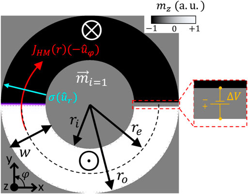
FIGURE 1. Scheme showing the relaxed states of spins in sub-lattice i = 1, in the positive z-direction (white domain), in the negative z-direction (black domain) and in the plane of the strip for an “Up to Down” (UD) domain wall (purple) according to the current direction, for an exemplary curved strip. The direction of the applied electric current (red arrow) in the Heavy Metal beneath the magnetic strip, generated from a potential difference ΔV (see inset), is shown as well as the geometrical parameters of the strip.
In Eq. 1,
In order to illustrate the current-driven DW dynamics along curved HM/FiM stacks we fix tFiM = 6 nm, and samples with different widths (w) and radii (re) were evaluated. The following common material parameters were adopted for the two sublattices i: 1, 2: Ai = 70 pJ/m, Ku,i = 1.4 × 10⁶ J/m3, αi = 0.02, Di = 0.12 J/m2, θSH,i = 0.155. The strength of the antiferromagnetic coupling between the sublattices was fixed to Bij ≡ B12 = − 0.9 × 10⁷ J/m3. The gyromagnetic ratios (γi = giμB/ℏ) are different due to the different Landé factor: g1 = 2.05 and g2 = 2.0. The saturation magnetization of each sublattice Ms,i can be tuned with the composition of the FiM and/or with the temperature of the ambient (T). Here, we assume the following temperature dependences for each sublattice:
3 Micromagnetic Results
Due to the several combination of parameters to consider in our study, we divided this section in three sub-sections: (A) The study on the influence of the strip width (w); (B) the study on curvature
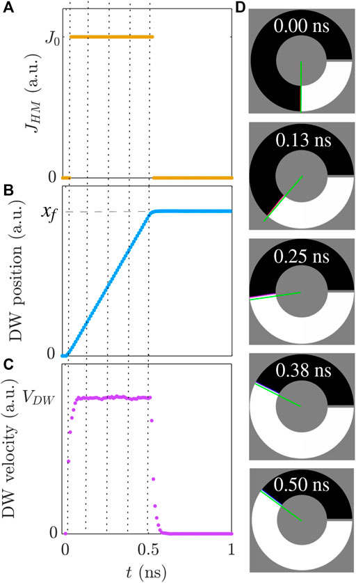
FIGURE 2. Micromagnetic results of applying a uniform JHM = J0 = 2 TA/m2 (A) showing the relative and final position xf (B) and velocity VDW (C), as a function of time t, of an UD DW in a curved strip (w = 256 nm and re = 384 nm), at T = 260 K. Insets (D) are snapshots of the magnetic configuration in sublattice i = 1 at different times [highlighted by the vertical dotted lines in (A–C)]. Green solid lines are for guiding the eye and are co-parallel with the strip radius.
3.1 Influence of Width for a Fixed Curvature
In this study, the curvature is fixed (re = 384 nm) and width (w) is varied from 56 to 296 nm in steps of 40 nm. Figure 3 shows the results for the terminal DW velocity (|VDW,i|) as a function of the nominal density current JHM = j0, equivalent to the homogeneous density current in a straight strip with the same cross-section. In the next sections, we use the notation JHM = J for simplicity. Figure 3 shows that temperature has a noticeable effect on the terminal velocity on the DW type equally, Up to Down domain (UD) or Down to Up domain (DU). As it was expected from previous work on straight FiM strips [11, 13], at TA the DW velocities are greater. Also, the DW velocities increase for narrower strips (red symbols). In fact, the observed trend is very similar to straight strips: the terminal velocity is maximum at the temperature of AMC, TA = 260 K and significantly increased, exceeding 2000 m/s for the narrowest strip as compared to ∼1800 m/s for the widest. These results also suggest that the DWs velocities are equal for both types of DWs (UD and DU), which would lead to no distortion of the size of a domain between two adjacent DWs travelling along the curved strip. This result is significantly different from FM systems [11].
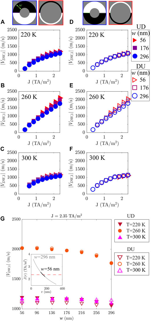
FIGURE 3. Terminal velocities as a function of J for a UD (A–C) and a DU (D–F) DW obtained for sub-lattice i = 1 and for three different temperatures: below, above and at the AMC temperature (220, 300, and 260 K, respectively). Strips for the two limiting cases are shown in the red and blue contour insets at the top. (G) Terminal velocities as a function of w for a UD (full symbols) and a DU (open symbols) type wall for J = 2.35 TA/m2 and the three chosen temperatures. Inset in (G) shows J(r) for two values of w. Red dashed line indicates J = 2.35 TA/m2.
At T ≠ TA, the DW velocity is reduced either increasing or reducing temperature with respect to TA, leading to velocities around 1100 m/s, generally regardless of the width and DW type. For a given J value, as the strip gets wider, however, the velocity is slightly smaller but these differences are negligible (see Figures 3A,C,D,F). This result contrasts with that of a FM strip, where a greater difference of velocities between a DU and a UD along a curved strip was shown [11].
To characterize the inertial motion of the DW, we evaluate the temporal evolution of the DW velocity [V(t), computed from the spatial averaging of m1,z(t)] as a function of time (or instant velocity) under a current square pulse of duration 0.1 ns and start at t = 0. The μm results can be fitted to the following exponentials:
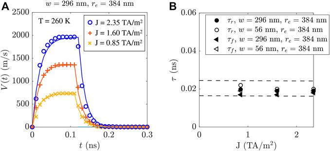
FIGURE 4. Instantaneous DW velocities V(t) for three values of J and for a curved strip of re = 384 nm and w = 296 nm at T = TA (A). Symbols are the μm data, from which τ (rise and fall times) are extracted for the narrowest and widest strips (B). Dashed lines in (B) are the upper and lower bounds of a 95% confidence interval.
Although simulations were performed for both types of DWs, note that we only present here results for the DU type wall, for sake of simplicity. Identical results (not shown) were obtained for the UD DW. Figure 4A show the “instantaneous” DW velocity V(t) and the relaxation times τ for three selected values of J (see solid symbols) at T = TA for the widest strip (w = 296 nm). Solid lines are the exponential curves to which the obtained simulated data is fit. For each current, the minimal τ is expected for T = TA = 260 K. Figure 4B shows that τr and τf for the two limiting cases (w = 56 nm and w = 296 nm) are quantitatively similar, in the order of 0.02 ns, since they fall within the 95% confidence interval, set by the largest error bars obtained for τ from the fitted results, among all J. Also, all values are similar in order to the step-size used in simulations, 0.01 ns (see Figure 4D).
Similar values of τ were obtained for strips of other widths. Relaxation times are not noticeably influenced by temperature, and they generally remain within the range of 0.01 ∼0.03 ns for T = 200 K and T = 300 K. This is more than one order of magnitude smaller than in FM strips, the latter being about
3.2 Influence of Curvature for a Fixed Width
In this study, the strip width is fixed to w = 256 nm and the curvature parameter ρ is varied. In other words, the equivalent radii re (re = ρ−1) is varied from 134 to 534 nm in steps of 50 nm. Figure 5 shows the results for the terminal velocity (|VDW,1|) of DU and UD DWs, for several values of re in nanometers, where the red (blue) curve corresponds to the smaller (greater) values, for three different temperatures.
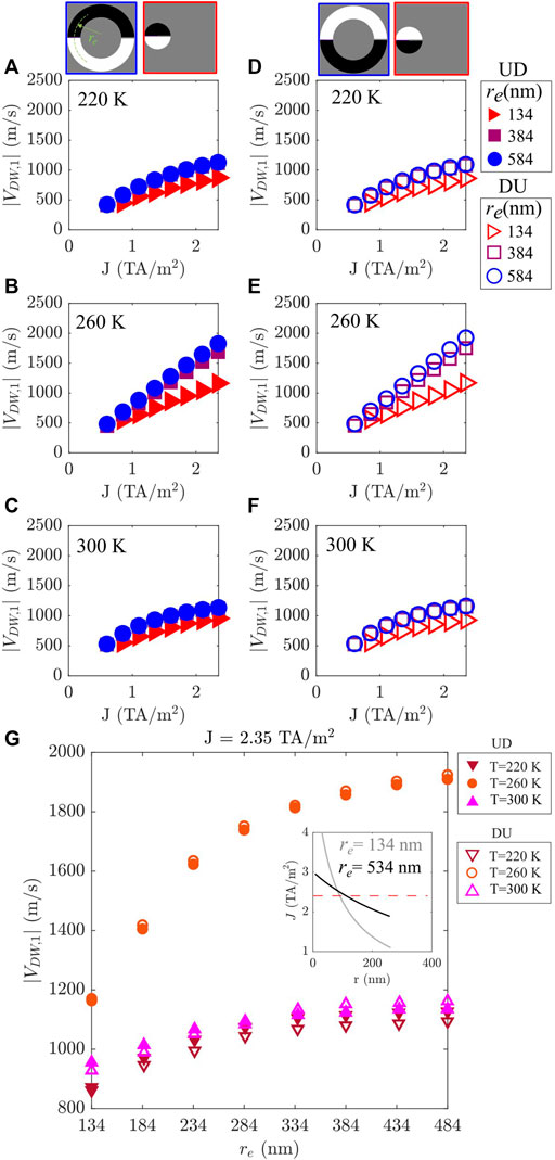
FIGURE 5. Terminal velocities as a function of J for a UD (A–C) and a DU (D–F) DW in the curved strip obtained for sub-lattice i = 1 and for three different temperatures: below, above and at the AMC temperature (220, 300, and 260 K, respectively). Strips for the two limiting cases are shown in the red and blue contour insets at the top. (G) Terminal velocities as a function of re for a UD (full symbols) and a DU (open symbols) type wall for J = 2.35 TA/m2 and the three chosen temperatures. Inset in (G) shows J(r) for two values of re. Red dashed line indicates J = 2.35 TA/m2.
Figures 5A–F shows that, at T = TA and for a given curvature, the DW velocities of DU and UD types are very similar for the whole range of currents explored. DW velocity reduces as the curvature increases (see Figure 5G). It is worth noting that the latter cannot be a consequence of only a nonuniform J(r) as defined in [11]. In fact, for curved-most strips (re = 134 nm), the spatial-dependent density current J(r) varies with r similarly as it does for changing w (see inset in Figures 3G, 5G), which would suggest similar variations to DW velocities as those found in Figure 3G. In other words, the impact of the non-uniform J(r) is not so relevant to be the only source of the big differences between the DW velocities for large and small curvatures (orange symbols in Figure 5G for re = 134 nm and re = 484 nm, respectively). Figure 5G also shows that as the strip curvature is reduced, DW velocity converges to the straight strip case (re → ∞).
For T ≠ TA, the dependence of the DW velocity with temperature is minimal regardless of the DW type. As the strip curvature increases there is a prominent change in the maximal terminal DW velocity for both DW types. However, the relative difference of velocities is almost negligible. Therefore, results suggest that the strip curvature affects in a similar way to width, and equally, to both DWs. In other words, the terminal velocity is significantly reduced as curvature (or width) increases, while the differences between DWs remain negligible (see Figure 5G). This behavior is even more pronounced at T = TA. As discussed in Section 3. A, the latter would imply that the robustness of a transmitted bit, encoded in a domain between two DWs, can be optimised in such curved-most strips and reaches larger velocities in the strip.
Figure 6A show the DW velocity as a function of time and for three selected values of J for an effective radius of re = 534 nm (least curved strip) and intermediate width w = 256 nm, at T = TA. Results look quantitatively similar to those shown in Figure 4A, where re was fixed to an intermediate value of 384 nm.
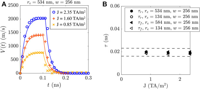
FIGURE 6. Instantaneous DW velocities V(t) for three values of J and for a curved strip of re = 584 nm and w = 256 nm at T = TA (A). Symbols are the μm data, from which τ (rise and fall times) are extracted for the narrowest and widest strips (B). Dashed lines in (B) are the upper and lower bounds of a 95% confidence interval.
As in Figures 4B, 6B shows that τr and τf for the two limiting cases (re = 134 nm and re = 534 nm) are quantitatively similar, in the order of 0.02 ns. For all the FiM curved strips explored at, above and below AMC, τr and τf remain within the range of 0.01 ∼0.03 ns, approximately one order of magnitude less than their FM counterparts. This is in good agreement with results presented in the previous section and other work in straight strips [8], which further supports the negligible inertia of DWs in such FiM systems.
3.3 Discussion on the Effective Influence of a Curved Shape on the Wall Velocity
A non-uniform current distribution is expected to influence the terminal velocity of the DW for a given curvature, specially for wide curved strips [11]. In this section, to explore further the degree of influence of the non-uniform current, equivalent studies on w and ρ on a straight strip with an artificially implemented non-uniform J(r = y) at T = TA are performed. A straight strip is a bounding case for a curved strip that shows no effective curvature (re → ∞, ρ → 0) and an homogeneous density current J = J0. Therefore, we explore whether “curvature (ρ) effects” are mainly dominated by the intrinsic inhomogenous current, or whether they can also arise from the curved shape itself [24]. We aim to discern the actual influence of an inhomogeneous current, as part of an more global effect due to the curved shape. For the following study, and since the straight shape must be retained, re (or equivalently ρ) is artificially modified in the non-uniform current distribution expression:
Figures 7A,B show the velocity of an UD wall in the straight strip for J = J0 = 2.35 TA/m2 (black crosses) and for an inhomogeneous J(y) (blue circles), varying re in J(y, re) (see insets) for a fixed width w = 256 nm, and varying width (w) for a fixed re, J(y, re = 384). While it is expected that an inhomogeneous J(y, w, re) will influence the DW velocity [especially for curved-most strips, see re = 134 nm in (a)], the differences with the case of J = J0 are almost negligible. Figures 7C,D show results for curved strips. For these cases, w and re are naturally varied in J(r, w, re) by modifying the shape itself. From the standpoint of the applied current, this is expected to be equivalent to doing it by changing the shape itself. Results from an inhomogeneous current (blue circles, reproduced from Figures 3G, 5G) consistently tend to converge to the straight strip as ρ is reduced. The strip is straight when ρ = 0 (re → ∞).
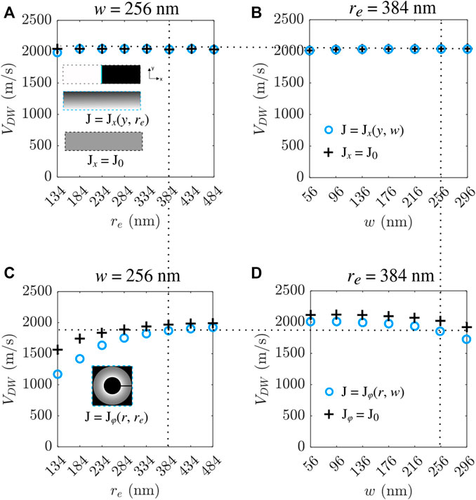
FIGURE 7. DW terminal velocities in a straight strip for an inhomogeneous J(y, w, re) (blue circles) and for a uniform J0 (black crosses) as a function of radius re (A) and width w (B) at same temperature (T = 260 K). Insets in (A) show the magnetic configuration of sublattice i = 1 at t = 0 and schematics of the current spatial distribution in the strips as examples. (B) DW terminal velocities in a curved strips with the same parameters as a function of radius re (C) and width w (D). As an example, inset in (C) shows the radial dependence of an inhomogenous current distribution in such a strip. Dotted lines highlight the cases where the two geometrical parameters (w and re) are coincident among all the studies.
When the strip is either straight (a-b) or curved (c-d), for both studies (fixing w and varying re or vice-versa), the DW velocity is found to be the same when the geometrical parameters are coincident, i.e., w = 256 nm and re = 384 nm, as expected [see horizontal dotted lines in (a-b) or (c-d)]. However, when the shape is different, even in the cases when w and re are coincident (and therefore, J(w, re) is expected to also be the same), different DW velocities are obtained [see vertical dotted lines in (a-c) and (b-d)] below and slightly above 2000 m/s, respectively. Moreover, by modifying either re or w in the curved strip by directly changing its shape [see (c-d) and previous sections], there is a clear larger impact on DW velocity, than by artificially (but equivalently) modifying re or w in the straight strip [see (a-c)]. In the curved strips, the trend when varying re or w is qualitatively similar regardless to the homogeneity of the applied J [see black crosses and blue circles in either (c) or (d)]. Since J(r) is modeled in an equivalent way in all studies by simply changing J(r) = J(y) for the straight strip, marked differences between the wall velocity in (a-b) (straight strip) and (c-d) (curved strip), specially for very curved strips, suggest that not only the non-uniform J(r) is influencing the UD DW motion.
Our results suggest that the curved shape may have an intrinsic influence on the wall velocity, manifested as a more marked dependence with w and re, regardless of the inhomogeneity of the current density [see Fig. (c–d)], as the shape becomes more curved. An influence due to the inhomogeneous current, still appears naturally in the curved strip, but may have a lesser impact compared to other geometrical factors (see differences between black crosses and blue circles).
4 Discussion and Summary
We have provided a study on DW motion in curved FiM strips, particularised to one of the two strongly coupled sub-lattices, for three different temperatures, and as a function of geometrical parameters for a HM/FiM/Ox multilayer structure. We observe an absence of tilting of the DW and domain distortion at different temperatures, 40 K above and below the angular momentum compensation temperature.
Width and curvature effects on the DW velocity are discussed. Besides contributions from a non-uniform J(r), there is an overall significant influence from the shape of the strip itself on DW velocity. This implies that, for a fixed temperature (or composition), DW velocity can be optimised by optimising the geometrical parameters of the curved strip. The relative differences between a DU and a UD walls are marginal in general. In other words, geometrical factors affect them almost equally, which is positive for a robust transmission of a bit encoded in an Up or Down domain between two adjacent DWs. With reducing current, differences in velocities between curved and straight strips are still minimised at the expense of slower DWs. Similar effect is observed as width or curvature is increased. This is beneficial for designing intricate 2D circuit tracks combining curved and straight sections, while preserving DW velocities still larger than those found in their FM counterparts. Also, DWs in a curved FiM strip show a negligible inertia in contrast to their FM counterparts (τFiM ≪ τFM) for all the explored scenarios. The DWs start to move and stop almost immediately (τFiM ∼ 0.02 ns) after the application or removal of current.
Considering the obtained results altogether and assuming T ≠ TA, which will be most of the experimental cases at room temperature (T = 300 K), our study allows us to conclude that narrow enough FiM strips are ideal candidates for designing curved tracks for 2D spintronic circuits of an arbitrary shape based on CDDWM, where bits are encoded in domains separated by walls. This is due to very fast rise and fall times (τr ∼ τf ≪ 0.1 ns), high velocities (VDW > 1000 m/s) and negligible distortion of the two types of DWs (UD and DU) in all the scenarios explored in this work. Greater DW terminal velocities and smaller time responses in curved FiM strips than those in their FM counterparts are obtained. These results can help in the further research, development and improvement of FiM-based spintronic circuitry that may require compactness and high-speed functionality with high robustness to DW (and/or domain) distortion.
Data Availability Statement
The raw data supporting the conclusion of this article will be made available by the authors, without undue reservation.
Author Contributions
DOR performed the micromagnetic simulations, designed the numerical experiments, performed the analysis of data and wrote the manuscript. VR provided with the micromagnetic code, OA and EM provided with the idea for the research and EM also contributed to the writing of the manuscript.
Funding
This work was supported by the project SA114P20 from Junta de Castilla y Leon (JCyL), and partially supported by the projects SA299P18 from JCyL, MAT2017-87072-C4-1-P and PID2020-117024GB-C41 from the Ministry of Economy, Spanish government, and MAGNEFI, from the European Commission (European Union). All data created during this research are openly available from the University of Salamanca’s institutional repository at https://gredos.usal.es/handle/10366/138189.
Conflict of Interest
The authors declare that the research was conducted in the absence of any commercial or financial relationships that could be construed as a potential conflict of interest.
Publisher’s Note
All claims expressed in this article are solely those of the authors and do not necessarily represent those of their affiliated organizations, or those of the publisher, the editors and the reviewers. Any product that may be evaluated in this article, or claim that may be made by its manufacturer, is not guaranteed or endorsed by the publisher.
References
1. Hubert A, Schäfer R. Magnetic Domains: The Analysis of Magnetic Microstructures. New York, NY, United States. Springer-Verlag Berlin Heidelberg (1998).
3. Parkin S, Yang S-H. Memory on the Racetrack. Nat Nanotech (2015) 10:195–8. doi:10.1038/nnano.2015.41
4. Miron IM, Moore T, Szambolics H, Buda-Prejbeanu LD, Auffret S, Rodmacq B, et al. Fast Current-Induced Domain-wall Motion Controlled by the Rashba Effect. Nat Mater (2011) 10:419–23. doi:10.1038/nmat3020
5. Emori S, Bauer U, Ahn S-M, Martinez E, Beach GSD. Current-driven Dynamics of Chiral Ferromagnetic Domain walls. Nat Mater (2013) 12:611–6. doi:10.1038/nmat3675
6. Haazen PPJ, Murè E, Franken JH, Lavrijsen R, Swagten HJM, Koopmans B. Domain wall Depinning Governed by the Spin Hall Effect. Nat Mater (2013) 12:299–303. doi:10.1038/nmat3553
7. Ryu K-S, Thomas L, Yang S-H, Parkin S. Chiral Spin Torque at Magnetic Domain walls. Nat Nanotech (2013) 8:527–33. doi:10.1038/nnano.2013.102
8. Torrejon J, Martinez E, Hayashi M. Tunable Inertia of Chiral Magnetic Domain walls. Nat Commun (2016) 7:13533. doi:10.1038/ncomms13533
9. Dzyaloshinsky I. A Thermodynamic Theory of "weak" Ferromagnetism of Antiferromagnetics. J Phys Chem Sol (1958) 4:241–55. doi:10.1016/0022-3697(58)90076-3
10. Garg C, Yang S-H, Phung T, Pushp A, Parkin S. Dramatic Influence of Curvature of Nanowire on Chiral Domain wall Velocity. Sci Adv (2017) 3:e1602804. doi:10.1126/sciadv.1602804
11. Alejos O, Raposo V, Martínez E. Domain wall Motion in Magnetic Nanostrips. In: Materials Science and Technology. Berlin, Germany. American Cancer Society (2020). p. 1–49. doi:10.1002/9783527603978.mst0459
12. Yang S-H, Ryu K-S, Parkin S. Domain-wall Velocities of up to 750 M S−1 Driven by Exchange-Coupling Torque in Synthetic Antiferromagnets. Nat Nanotech (2015) 10:221–6. doi:10.1038/nnano.2014.324
13. Siddiqui SA, Han J, Finley JT, Ross CA, Liu L. Current-Induced Domain Wall Motion in a Compensated Ferrimagnet. Phys Rev Lett (2018) 121:057701. doi:10.1103/physrevlett.121.057701
14. Caretta L, Mann M, Büttner F, Ueda K, Pfau B, Günther CM, et al. Fast Current-Driven Domain walls and Small Skyrmions in a Compensated Ferrimagnet. Nat Nanotech (2018) 13:1154–60. doi:10.1038/s41565-018-0255-3
15. Martínez E, Raposo V, Alejos Ó. Current-driven Domain wall Dynamics in Ferrimagnets: Micromagnetic Approach and Collective Coordinates Model. J Magnet Magn Mater (2019) 491:165545. doi:10.1016/j.jmmm.2019.165545
16. Arpaci S, Lopez-Dominguez V, Shi J, Sánchez-Tejerina L, Garesci F, Wang C, et al. Observation of Current-Induced Switching in Non-collinear Antiferromagnetic IrMn3 by Differential Voltage Measurements. Nat Commun (2021) 12:3828. doi:10.1038/s41467-021-24237-y
17. Landau L, Lifshitz E. On the Theory of the Dispersion of Magnetic Permeability in Ferromagnetic Bodies. Phys Zeitsch der Sow (1935) 8:153–69.
18. Martinez E, Emori S, Perez N, Torres L, Beach GSD. Current-driven Dynamics of Dzyaloshinskii Domain walls in the Presence of In-Plane fields: Full Micromagnetic and One-Dimensional Analysis. J Appl Phys (2014) 115:213909. doi:10.1063/1.4881778
19. Slonczewski JC. Current-driven Excitation of Magnetic Multilayers. J Magnet Magn Mater (1996) 159:L1–L7. doi:10.1016/0304-8853(96)00062-5
20. Alejos O, Raposo V, Sanchez-Tejerina L, Tomasello R, Finocchio G, Martinez E. Current-driven Domain wall Dynamics in Ferromagnetic Layers Synthetically Exchange-Coupled by a Spacer: A Micromagnetic Study. J Appl Phys (2018) 123:013901. doi:10.1063/1.5009739
21. Thiaville A, Nakatani Y, Piéchon F, Miltat J, Ono T. Transient Domain wall Displacement under Spin-Polarized Current Pulses. Eur Phys J B (2007) 60:15–27. doi:10.1140/epjb/e2007-00320-3
22. Gomonay O, Jungwirth T, Sinova J. High Antiferromagnetic Domain Wall Velocity Induced by Néel Spin-Orbit Torques. Phys Rev Lett (2016) 117:017202. doi:10.1103/physrevlett.117.017202
23. Selzer S, Atxitia U, Ritzmann U, Hinzke D, Nowak U. Inertia-Free Thermally Driven Domain-Wall Motion in Antiferromagnets. Phys Rev Lett (2016) 117:107201. doi:10.1103/physrevlett.117.107201
Keywords: spintronics, ferrimagnetism, spin-orbit coupling, micromagnetics simulation, domain walls
Citation: Osuna Ruiz D, Alejos O, Raposo V and Martínez E (2021) Current-Driven Domain Wall Motion in Curved Ferrimagnetic Strips Above and Below the Angular Momentum Compensation. Front. Phys. 9:772264. doi: 10.3389/fphy.2021.772264
Received: 07 September 2021; Accepted: 05 November 2021;
Published: 03 December 2021.
Edited by:
Xin Fan, University of Denver, United StatesReviewed by:
Robert James Joynt, University of Wisconsin-Madison, United StatesMantao Huang, Massachusetts Institute of Technology, United States
Copyright © 2021 Osuna Ruiz, Alejos, Raposo and Martínez. This is an open-access article distributed under the terms of the Creative Commons Attribution License (CC BY). The use, distribution or reproduction in other forums is permitted, provided the original author(s) and the copyright owner(s) are credited and that the original publication in this journal is cited, in accordance with accepted academic practice. No use, distribution or reproduction is permitted which does not comply with these terms.
*Correspondence: D. Osuna Ruiz, b3N1bmFydWl6LmRhdmlkQHVzYWwuZXM=
 D. Osuna Ruiz
 O. Alejos
 V. Raposo
 E. Martínez