 Lixia Tian
 Hao Li*
- Guangdong Provincial Key Laboratory of Optical Information Materials and Technology, Institute of Electronic Paper Displays, South China Academy of Advanced Optoelectronics, South China Normal University, Guangzhou, China
As a new reflective display technology, electrowetting displays (EWDs) have many important characteristics, such as high reflectivity, low power consumption, and paper-like display. However, the contact angle hysteresis, which is the inconsistency between the advancing contact angle and the receding contact angle of oil droplet movement, seriously affects the response speed of EWDs in the driving process. According to the hysteresis phenomenon of contact angle in an oil switch motion with the action of interface tension, the brightness curve of EWDs in the process of pixel switching by different driving voltages was tested in this paper, and driving voltage was changed from 30 to 100 V at the same time. Then, in order to reduce the influence of the hysteresis effect, an equivalent driving waveform design method with overdriving voltage was proposed, and the overvoltage was set to 100 V according to the hysteresis effect and driving characteristic of EWDs. Experimental results showed that the response rising time of EWDs was reduced to 21 ms by using the proposed driving waveform, and the response performance of EWDs can be effectively improved.
Introduction
Reflective display has become common in e-readers. The most successfully commercialized e-book reader was produced by Amazon and Sony. At present, electrowetting displays (EWDs) have excellent characteristics of high reflectivity [1], fast response [2, 3], and paper-like display and low power consumption [4, 5], which is completely superior to electrophoresis displays (EPDs) [6, 7]. Moreover, the manufacturing engineering of EWDs is based on the liquid crystal display, which makes it cost-effective and easier to manufacture [8, 9]. Therefore, many scholars and investors have been attracted by EWD technology.
EWDs can realize an optical switch by controlling the movement of colored oil films. It was first proposed and implemented by Hayes in 2003 and published in Nature [10]. When a pixel unit was on-switching or off-switching, the brightness curve corresponding to the splitting, moving, and restructuring of the oil film in pixels was usually called the on-off curve, which is also called the response curve of EWDs [11]. Response time refers to the response speed of EWDs for displaying gray scales. Generally speaking, the response time is divided into two parts: rising time and falling time, and the sum of the two is called the response time of EWDs. However, in a response process, the oil backflow and hysteresis could lead to a negative effect on reducing the response time of EWDs [12]. So, research on response time is of great significance to analyze the oil film hysteresis, backflow, interface mechanics, and electrodynamics of EWDs.
The hysteresis effect, which is caused by the inconsistent contact angle and the persistence of oil backflow, can increase the complexity of shortening the response time [13, 14]. In 2011, Yung [15] studied the method of controlling grayscales and fast response of EWDs and proposed an asymmetric gray scales driving scheme, which changed the hysteresis characteristic curve of EWDs. It not only accelerated the response time but also effectively suppressed the phenomenon of oil backflow. However, researchers did not further explore the parameters of response time and backflow. In 2015, Yi [16] used electrophoretic chips to drive a matrix EWD system and used a unipolar PWM waveform modulation to realize EWD gray scales display. And a reset sub-frame was set to release charge trapping for weakening the oil backflow phenomenon, so as to keep a stable on-state for a longer time in a pixel. But this method prolonged the response time. In 2019, Yi [17] adopted a method of amplitude-frequency mixed modulation to drive EWDs. The oil was driven at 30 V to quickly approach a target reflectivity, and then the driving voltage was reduced to stabilize the oil reflectivity to the target reflectivity. But the response time of EWDs was limited. Lately, Zeng [18] introduced a 4 ms overdriving stage at 32 V to improve the response speed of EWDs, but the situation of much higher overdriving voltages had not been studied. In addition, it did not give a general method to design a waveform, and the proposed waveform was only limited to the EWD used in its verification. Once the technological process of EWDs changes, it will result in an inevitable redesign of the waveform.
In this paper, by recording the brightness curve of EWDs during the on- and off-switching process, the influence of oil motion hysteresis on response time was analyzed, and the hysteresis phenomenon of EWDs was summarized. Then, a driving method with an equivalent driving constant for EWDs was proposed. Furthermore, an overvoltage driving waveform was designed to shorten the response rising time of EWDs. The proposed driving constraint method enabled overvoltage driving to be used in EWDs. The validity of this method was verified by experimental data.
Principles
Driving Principle of EWDs
The principle of EWDs is based on the movement of colored oil droplets by applying an external voltage [19–21]. Its essence is an optical switch [22]. The structure of an EWD is mainly composed of the glass substrate, indium tin oxide (ITO), hydrophobic insulator layer, pixel wall, colored oil, and water [23, 24]. The EWD operating principle and pixel structure are shown in Figure 1. When no driving voltage is applied between the electrodes, the colored oil film lies naturally between the water and the hydrophobic insulator layer; as shown in Figure 1A, the pixel is in a dark off-state. However, when a driving voltage is applied between the substrate electrode and the water, the oil film can be pushed aside by water with the electrowetting effect. As shown in Figure 1B, the reflective substrate electrode is exposed, different wavelengths of reflected light are superimposed to form a white optical sense, and the pixel is in a white on-state. In this way, the optical properties of the stack can be switched between a colored off-state and a white on-state [25, 26].
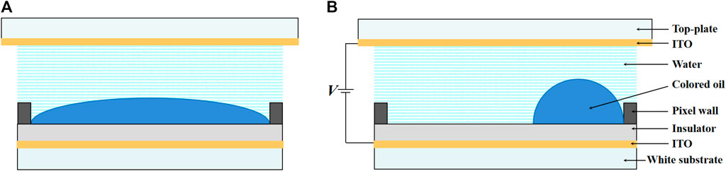
FIGURE 1. Driving principle and pixel structure of EWDs. The optical stack consists of the glass substrate, indium tin oxide (ITO), a hydrophobic insulator layer, pixel wall, colored oil, and water. (A) Without applied voltage, a homogeneous oil film is present and the pixel is in colored off-state. (B) With an applied voltage, the oil film is shrunk to a corner and the pixel is in white on-state.
Hysteresis Effect of EWDs
In a pixel, the inconsistency between the advancing contact angle and the receding contact angle of oil droplet movement results in the hysteresis of EWDs [27, 28]. On the non-ideal surface, the droplet is in a metastable equilibrium state. When the droplet is deformed, there is a difference between the forward contact angle and the backward contact angle. This phenomenon is called contact angle hysteresis. In EWDs, the hysteresis phenomenon of contact angle would lead to the hysteresis effect, which shows that the reflected light intensity curves of the EWDs cannot coincide in the open phase and the closed phase. The main reasons for hysteresis include slight fluctuation in the process of oil film rupture and recombination and the viscous dissipation between the oil and dielectric layer at the same time.
The fluctuation of oil film rupture in an on-switching process is mainly caused by the fluctuation inside the oil after applying an external electric field force. Figure 2 shows the process of oil film rupture in a pixel from off-state to on-state. During oil contraction, with the increase of the external force, the fluctuation amplitude can be increased. When the fluctuation is large enough, the oil film can be ruptured. This is related to the pixel structure and oil material parameters, as shown in Equations 1, 2 [29].
where
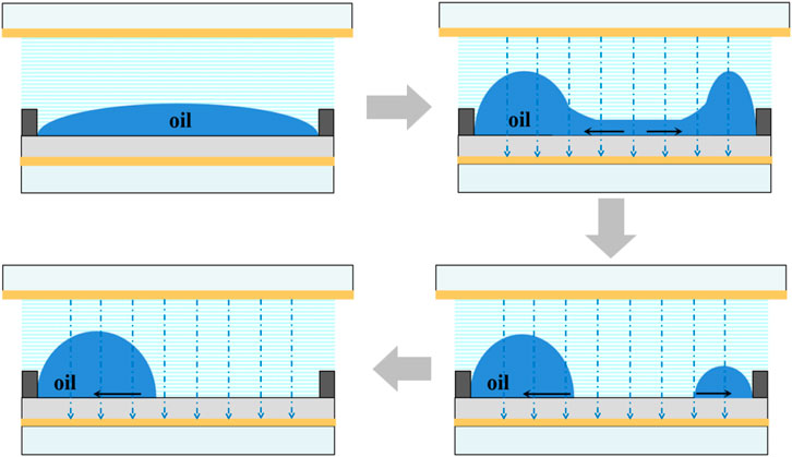
FIGURE 2. The process of oil film rupture in a pixel from off-state to on-state. For the on-switching process, after applying external electric field force, the oil film begins to rupture with slight fluctuation. The fluctuation amplitude becomes larger with the increase of external force, and then, the oil can be shrunk to corners.
The oil recombination process is the off-switching stage of an EWD pixel, as shown in Figure 3. The capillary force existing in the oil/water interface and the net force on the contact line are key elements in this reforming process. The timescale
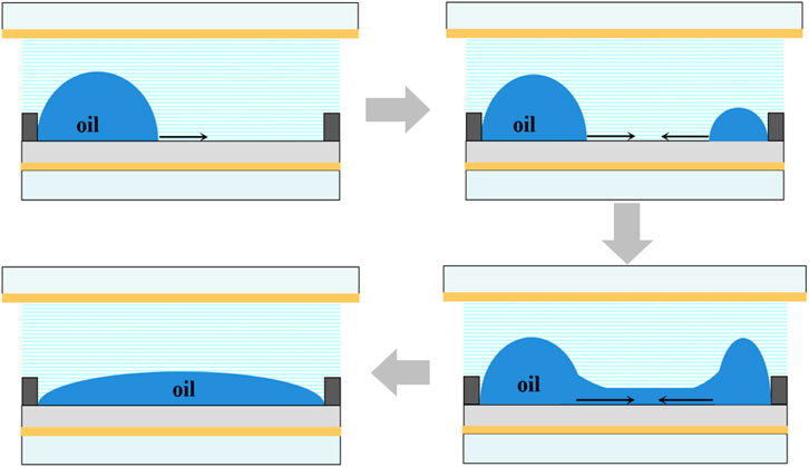
FIGURE 3. The process of oil film recombination in a pixel from on-state to off-state. For the off-switching process, when the driving voltage is decreased, the oil begins to recombine with slight fluctuation, and the oil is spread out in the pixel gradually.
The oil recombination time is inversely proportional to the thickness of the oil film. When the oil film fluctuation is much smaller than the thickness of the film, the equation is strictly valid. However, when the thickness of oil becomes thinner, the hysteresis effect can be increased dramatically. In the driving process, the thickness of the oil film varies as the voltage becomes larger. When the voltage is removed, the oil reforming time will be affected by different potential energy in the recombination process. When the conductive liquid contacts with the hydrophobic insulator layer, there is a resistance force in the three-phase contact line among the hydrophobic insulator layer, the oil, and the conductive liquid. This is because the surface of the hydrophobic dielectric insulation is not completely smooth. The force which hinders the oil movement in the three-phase contact line can lead to viscous dissipation.
A C-V curve for a segment of an EWD panel was shown in Figure 4. In the process of driving colored oil in pixels, when the driving voltage increased from 0 to 40 V, the colored oil film changed from lipophilic to hydrophilic. At the same time, with the combined action of electric field force, the polar liquid oil film ruptured and gradually gathered to corners. Ideally, the oil film would gather in a pixel corner. In this process, the voltage at the point at which the oil film began to be ruptured was called the threshold voltage. Above the threshold voltage, the optical response could be increased gradually. When the driving voltage decreased from 40 to 0 V, the optical response decreased linearly. The oil film rewets the interface until the fluoropolymer surface was completely covered. There was a clear hysteresis between switching-on and switching-off electro-optic curves.
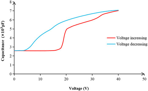
FIGURE 4. | Hysteresis characteristic curve of an EWD panel. A step voltage from 0 to 40 V was used to measure the rising edge curve. The step time was 2 s and the step voltage was 2 V. A step voltage from 40 to 0 V was used to measure the falling edge curve. The step time was 2 s and the step voltage was −2 V.
Experimental Results and Discussion
Optical Measurement Platform
To measure the Luminance-Time relationship of EWDs, a response testing platform was set up as shown in Figure 5. The main optical measuring equipment was a colorimeter (Arges-45, Admesy, Netherlands) which was used to measure the EWD luminance. Its measuring speed is 10,000 times/s, and the size of the measuring point is 3 mm. The optical system adopted a 45-degree incident light source and a 90-degree measuring angle. It was connected with a computer (M425, Lenovo, China) to save and display measured data graphically. In addition, experimental equipment also included a function waveform generator (AFG3052C, Tektronix, United States), an amplifier (ATA-2022H, Agitek, China), and a microscope (XTL-165, Phenix, China). The system used an adjustable DC power supply for providing a voltage that could change from 0 to 30 V. Programmable driving voltages were generated by the function waveform generator in combination with the voltage amplifier. And the fluidic pattern in pixels was recorded by the camera with a microscope synchronously. This system could record the brightness change of the reflected light during the driving process of EWDs.
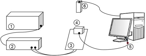
FIGURE 5. The response testing platform of EWDs. ① Waveform generator. ② Voltage amplifier. ③ EWD panel. ④ Colorimeter. ⑤ Computer. ⑥ Microscope.
In the tested EWD panel, Teflon AF1600 was used as the hydrophobic insulator layer material. The insulator was spin-coated on the ITO glass substrate with a resistivity of 100 Ω Sq. Transparent polyimide was used as the grid material of pixel walls and the photoresist was Microchem SU8 3005. The conductive fluid was NaCl with a concentration of 0.001 M. The parameters of the EWD panel used in the experiment were shown in Table 1.

TABLE 1. Parameters of the EWD panel.
Driving Waveform Design
Driving waveforms were designed to study the influence of the hysteresis effect and oil backflow on the response time of EWDs; the response time of the traditional driving scheme and that of equivalent voltage driving scheme were compared. In the experiment, with the increase of voltage, the reflected brightness curve of EWDs became steeper from off-state to on-state. However, from on-state to off-state, the reflected brightness of EWDs was decreased with the rewetting of the oil. Finally, the oil was tiled again in the pixel.
As shown in Figure 6, when the applied DC voltage was 100 V and the EWD was driven for 15 ms, the reflected light intensity of the EWD was stronger than that of the low voltage. When pixels were observed with a microscope, the aperture ratio of the pixel was increased from 60% (at 30 V) to 65% (at 100 V), but the oil film overflowed to the pixel wall after the voltage driving, resulting in an increase of the light transmission intensity of pixels, and this process was irreversible. Through the analysis of the brightness curve, the brightness value could not be restored to the value before power on. At the same time, the slope of the descent curve could be changed and the descent time was prolonged.
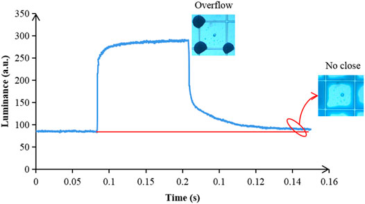
FIGURE 6. The brightness curve of an EWD driven by a DC voltage for 15 ms. The applied driving voltage was 100 V. The oil film overflowed to the pixel wall, and it could not cover the whole pixel even power off.
In order to prevent the oil film from overflowing, an equivalent driving constant E = UT was designed, where U was the driving voltage, and T is the driving time of no oil film overflowing to the pixel wall. In this case, T was defined as the time when the oil film was driven from 0 to 90% of the maximum pixel aperture. As shown in Figure 7, the EWD was driven at 30 V, T was 44 ms, and then, the equivalent driving constant E was 1,320. When the product of applied voltage and driving time was greater than the equivalent driving constant, the oil film shrinkage state could exceed the limit. Excessive electric field force would make the oil film overflow the pixel wall, resulting in a reduction of the oil film. When the pixel was closed, some areas could not cover with the oil film, which showed that the pixel was always in on-state. Figure 8 showed a top view of oil film when oil overflowed to the pixel wall with a high voltage.
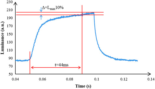
FIGURE 7. The switch response curve of EWDs with a 30 V driving voltage and the calculation diagrammatic sketch of the constant E.
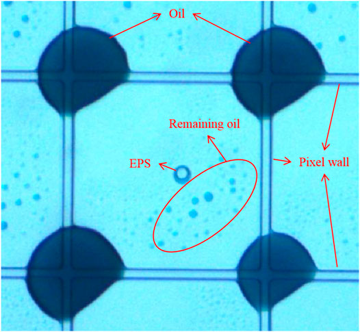
FIGURE 8. Top view of pixels when the oil film overflowed to the pixel wall. When the EWD panel was driven by a high voltage, the oil film gathered on the pixel wall. When the driving voltage was removed, the amount of oil film in the pixel grid changed, and the oil film could not cover the whole pixel, which made the pixel unable to close. The circle in the middle of the pixel was an extra pinning structure (EPS). The random black spots in pixels were the residual oil.
Figure 9 showed brightness-time curves of an EWD when it was turned on and off with applied voltages of 40, 60, 80, and 100 V. After switching off the device, the brightness value could return to the value before the EWD was turned on, which proved that the equivalent driving method could make EWDs work without being damaged. With the constraint of the equivalent driving constant 1,000, the driving times were 25, 16, 12, and 10 ms, respectively, when the applied voltages were 40, 60, 80, and 100 V. The larger the driving voltage was, the steeper the rising edge of the response curve was. Meanwhile, the aperture ratio was larger, and the light reflection intensity of the pixel was higher. The response rising time took 1.2 ms for 100 V driving voltage, 1.95 ms for 80 V driving, 3.9 ms for 60 V driving, and 10.7 ms for 40 V driving. With the increase of driving voltage, the pixel opening time decreased exponentially, as shown in Figure 10.
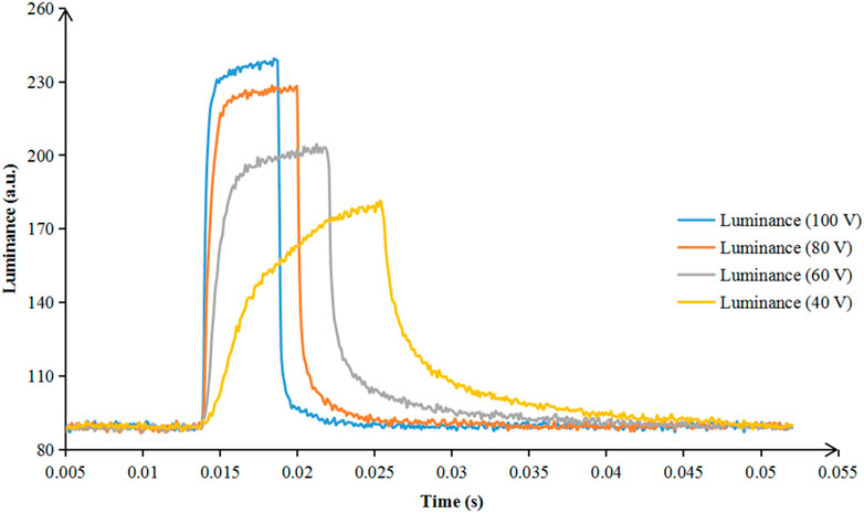
FIGURE 9. Comparison of oil film opening time among different voltages with equivalent driving constraints. The larger the driving voltage, the steeper the rising edge of the response curve.
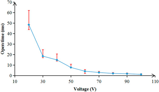
FIGURE 10. The relationship between driving voltage and pixel opening time. The dot in the figure represented the response rising time of the pixel when the applied driving voltage was from 20 to 100 V. The pixel opening time was decreased exponentially with the increase of driving voltage.
Figure 11 showed the comparison of the oil film closing process with different driving voltages. The falling curve was a process of pixel closing. The larger the pixel aperture ratio, the higher the concentration height of the oil film. And the potential energy of the oil film in a pixel was larger, which made the timescale of rewetting shorter when it was in the off-switching process. When the EWD panel was driven by 40, 60, 80, and 100 V, the oil film closing time was 31.7, 24.6, 14.8, and 10.9 ms, respectively. Figure 12 showed the relationship between the driving voltage and the oil film closing time. The larger the driving voltage, the shorter the closing time. The curve showed an obvious linear relationship.
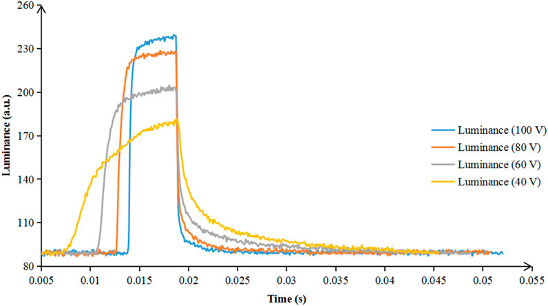
FIGURE 11. Comparison of oil film closing time among different driving voltages with equivalent driving constraints. The larger the pixel aperture ratio, the faster of rewetting the whole pixel.
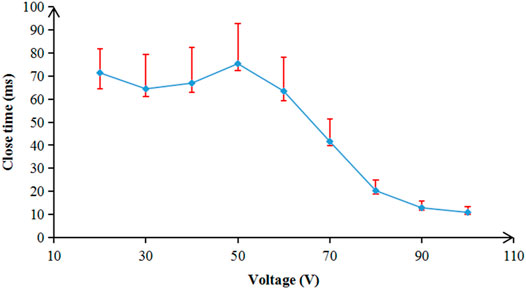
FIGURE 12. The relationship between different driving voltages and oil film closing time. The dot in the figure represented the closing time of the pixel when the applied driving voltage was from 20 to 100 V. The larger the driving voltage, the shorter the closing time.
The overvoltage driving waveform was shown in Figure 13. The proposed driving waveform was divided into two stages, including 100 and 11 V driving voltages. In the first stage, an overdriving voltage was used to accelerate the oil film motion. The pixel opening time was reduced by an overdriving voltage (100 V). The driving waveform of the second stage was used to maintain the pixel opening state and maintain the aperture ratio by a normal driving voltage (11 V). In Figure 13, the driving time in the first stage was 10 ms, and the oil film stabilization time was 11 ms in the second stage, which shortened the pixel opening time of 11 V to 21 ms, and it improved the response performance of a pixel.
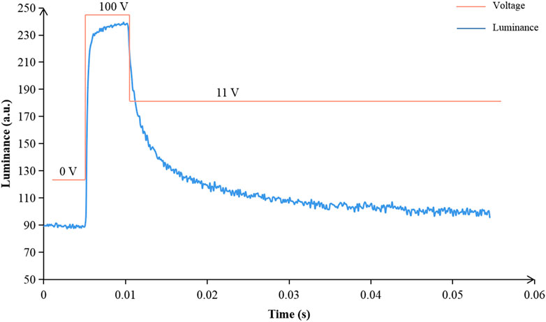
FIGURE 13. Diagram of an overvoltage driving waveform and the response curve of EWDs with a 100 V overvoltage. The proposed driving waveform contained two stages. The first stage was an overvoltage for accelerating the oil film motion. The second stage was used to maintain the pixel opening state by a normal driving voltage.
When the overvoltage was 100 V in the first stage, the luminance curve of an EWD driven by different voltages from 9 to 30 V in the second stage was shown in Figure 14. The lower driving voltage in the second stage had little effect on the pixel opening time. However, the pixel opening time increased exponentially with the decrease of driving voltage when the EWD panel was driven by a DC voltage. Moreover, due to the hysteresis characteristic of EWDs, it was difficult to turn on pixels at a low DC voltage. On the contrary, the proposed driving waveform could still turn on pixels at 9 V. That is to say, the proposed driving waveform significantly improved the lowest aperture of pixels and enhanced the grayscale display ability of EWDs.
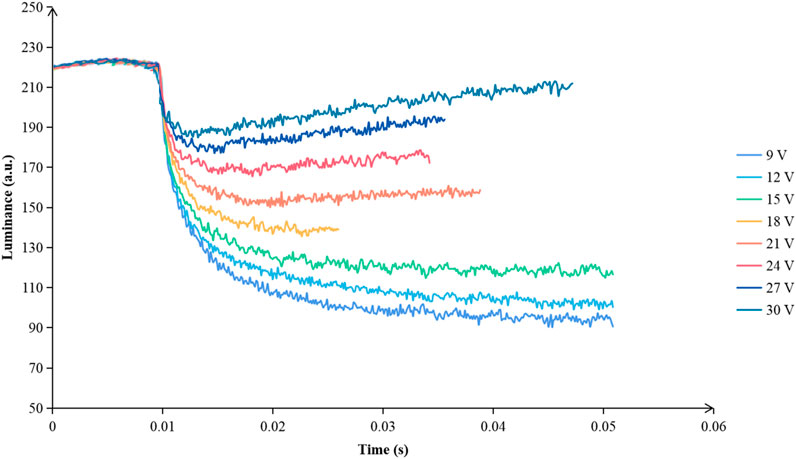
FIGURE 14. The brightness curve of an EWD which was driven by different voltages from 7 to 21 V in the second stage. The lower the driving voltage, the more obvious reduction of pixel opening time.
Conclusion
In this paper, an equivalent driving waveform design method was proposed according to the driving hysteresis characteristics of EWDs. The brightness changes of an EWD pixel during the switching process were statistically analyzed, and the equivalent driving constants were proposed as parameters for driving waveform design. Response curves of the pixel switching process with different driving voltages from 30 to 100 V were analyzed experimentally. It was proved that the equivalent driving constant could effectively protect EWDs from damage. Meanwhile, the overvoltage driving waveform of 100 V was designed to shorten the response rising time to 21 ms with an 11 V driving voltage. The proposed driving waveform could improve the display performance of pixels and facilitate the process of market application of EWDs.
Data Availability Statement
The original contributions presented in the study are included in the article/supplementary material; further inquiries can be directed to the corresponding author.
Author Contributions
LT and HL designed this project. LT carried out most of the experiments. HL performed part of the experiments and helped with discussions during manuscript preparation. LT contributed to the data curation and analysis. HL provided helpful discussions on the experimental results. All authors contributed to the article and approved the submitted version.
Funding
This article is supported by the Program for Guangdong Innovative and Entrepreneurial Teams (No. 2019BT02C241), Science and Technology Program of Guangzhou (No. 2019050001), Program for Chang Jiang Scholars and Innovative Research Teams in Universities (No. IRT_17R40), Guangdong Provincial Key Laboratory of Optical Information Materials and Technology (No. 2017B030301007), Guangzhou Key Laboratory of Electronic Paper Displays Materials and Devices (201705030007), and MOE International Laboratory for Optical Information Technologies and the 111 Project.
Conflict of Interest
The authors declare that the research was conducted in the absence of any commercial or financial relationships that could be construed as a potential conflict of interest.
Publisher’s Note
All claims expressed in this article are solely those of the authors and do not necessarily represent those of their affiliated organizations, or those of the publisher, the editors, and the reviewers. Any product that may be evaluated in this article, or claim that may be made by its manufacturer, is not guaranteed or endorsed by the publisher.
References
1. Heikenfeld J., Zhou K., Kreit E., Raj B., Yang S., Sun B, et al. Electrofluidic displays using Young-Laplace transposition of brilliant pigment dispersions. Nat Photon (2009) 3(5):292–6. doi:10.1038/NPHOTON.2009.68
2. Qian M, Lin S, Zeng S, Lin Z, Guo T, Tang B. Real-time dynamic driving system implementation of electrowetting display. Opto-Electronic Eng (2019) 46(06):87–95. doi:10.12086/oee.2019.180623
3. Yi Z., Zeng W., Ma C., Feng H., Yang J., Liu L, et al. A real‐time touch control system design based on field‐programmable gate array via optimizing Bresenham algorithm for electrowetting displays. J Soc Inf Display (2021) 29(7):573–83. doi:10.1002/jsid.1001
4. Li W., Wang L., Zhang T., Lai S., Liu L., He W, et al. Driving Waveform Design with Rising Gradient and Sawtooth Wave of Electrowetting Displays for Ultra-Low Power Consumption. Micromachines (2020) 11(2):145. doi:10.3390/mi11020145
5. Liu L., Bai P., Yi Z., Zhou G. A Separated Reset Waveform Design for Suppressing Oil Backflow in Active Matrix Electrowetting Displays. Micromachines (2021) 12(5):491. doi:10.3390/mi12050491
6. Shen S., Gong Y., Jin M., Yan Z., Xu C., Yi Z, et al. Improving electrophoretic particle motion control in electrophoretic displays by eliminating the fringing effect via driving waveform design. Micromachines (2018) 9(4):143. doi:10.3390/mi9040143
7. Wang L., Yi Z., Jin M., Shui L., Zhou G. Improvement of video playback performance of electrophoretic displays by optimized waveforms with shortened refresh time. Displays (2017) 49(9):95–100. doi:10.1016/j.displa.2017.07.007
8. Tröls A., Enser H., Jakoby B. Modeling and fabrication of low-cost electrowetting actuators for flexible microfluidic display applications. IEEE SENSORS (2016) 10:1–3. doi:10.1109/ICSENS.2016.7808429
9. Zhao R., Cumby B., Russell A., Heikenfeld J. Large area and low power dielectrowetting optical shutter with local deterministic fluid film breakup. Appl Phys Lett (2013) 103(33):223510. doi:10.1063/1.4834095
10. Hayes R. A., Feenstra B. J. Video-speed electronic paper based on electrowetting. Nature (2003) 425(6956):383–5. doi:10.1038/nature01988
11. Palanivelu S, Surjya S. Display Applications of Electrowetting. J Adhes Sci Tech (2012) 26(12-17):1947–63. doi:10.1163/156856111X600532
12. Yi Z., Huang Z., Lai S., He W., Wang L., Chi F, et al. Driving Waveform Design of Electrowetting Displays Based on an Exponential Function for a Stable Grayscale and a Short Driving Time. Micromachines (2020) 11(3):313. doi:10.3390/mi11030313
13. Zhang X-M., Bai P-F., Hayes R., Shui L-L., Jin M-L., Tang B, et al. Novel driving methods for manipulating oil motion in electrofluidic display pixels. J Display Technol (2015) 12(2):1. doi:10.1109/jdt.2015.2477947
14. Lin S., Zeng S., Qian M., Lin Z., Guo T., Tang B. Improvement of display performance of electrowetting displays by optimized waveforms and error diffusion. J Soc Inf Display (2019) 27(10):619–29. doi:10.1002/jsid.790
15. Chiu Y-H., Liang C-C., Chen Y-C., Lee W-Y., Chen H-Y., Wu S-H. Accurate-gray-level and quick-response driving methods for high-performance electrowetting displays. J Soc Inf Display (2011) 19(11):741–8. doi:10.1889/JSID19.11.741
16. Yi Z., Shui L., Wang L., Jin M., Hayes R. A., Zhou G. A novel driver for active matrix electrowetting displays. Displays (2015) 37:86–93. doi:10.1016/j.displa.2014.09.004
17. Yi Z., Liu L., Wang L., Li W., Shui L., Zhou G. A Driving System for Fast and Precise Gray-Scale Response Based on Amplitude-Frequency Mixed Modulation in TFT Electrowetting Displays. Micromachines (2019) 10(11):732. doi:10.3390/mi10110732
18. Zeng W., Yi Z., Zhao Y., Zeng W., Ma S., Zhou X, et al. Design of Driving Waveform Based on Overdriving Voltage for Shortening Response Time in Electrowetting Displays. Front Phys (2021) 9(642682):1–9. doi:10.3389/fphy.2021.642682
19. Roques C, Hayes R, Feenstra B, Schlangen L. Liquid behavior inside a reflective display pixel based on electrowetting. J Appl Phys (2004) 95(8):4389–96. doi:10.1063/1.1667595
20. Yi Z., Feng H., Zhou X., Shui L. Design of an Open Electrowetting on Dielectric Device Based on Printed Circuit Board by Using a Parafilm M. Front Phys (2020) 8(193):1–10. doi:10.3389/fphy.2020.00193
21. Zhang C. Z., Yi Z, de Rooij N, de Rooij N., Zhou G., Gravina R. Editorial: Modeling and Applications of Optoelectronic Devices for Access Networks. Front Phys (2021) 9(678269):1–3. doi:10.3389/FPHY.2021.678269
22. Yi Z., Feng W., Wang L., Liu L., Lin Y., He W, et al. Aperture ratio improvement by optimizing the voltage slope and reverse pulse in the driving waveform for electrowetting displays. Micromachines (2019) 10(12):862. doi:10.3390/mi10120862
23. Feenstra J. Video-Speed Electrowetting Display Technology. Handbook Vis Display Tech (2016) 1(13):2443–58. doi:10.1007/978-3-319-14346-0_103
24. Jin M., Shen S., Yi Z., Zhou G., Shui L.. Optofluid-Based reflective displays. Micromachines (2018) 9(4):159. doi:10.3390/mi9040159
25. Feenstra B. J., Hayes R. A., Camps I. G. J., Hage L. M., Johnson M. T., Roques-Carmes T, et al. A video-speed reflective display based on electrowetting: principle and properties. J Soc Inf Display (2004) 12(3):293–9. doi:10.1889/1.1825703
26. Jung H-Y., Choi U-C., Park S-H., Hwang H-S., Park C-W., You B-H, et al. P-48: Development of Driver IC with Novel Driving Method for the Electrowetting Display. SID Symp Dig Tech Pap (2012) 43(1):1239–42. doi:10.1002/j.2168-0159.2012.tb06022.x
27. Li W., Wang L., Henzen A. A Multi Waveform Adaptive Driving Scheme for Reducing Hysteresis Effect of Electrowetting Displays. Front Phys (2020) 8(618811):1–10. doi:10.3389/fphy.2020.618811
28. Berthier J. Electrowetting Theory. In: Micro-Drops and Digital Microfluidics. Amsterdam, Netherlands: Elsevie (2013). p. 161–224. doi:10.1016/B978-1-4557-2550-2.00004-3
29. Zhou M., Zhao Q., Tang B., Groenewold J., Hayes R. A., Zhou G. Simplified dynamical model for optical response of electrofluidic displays. Displays (2017) 49:26–34. doi:10.1016/j.displa.2017.05.003
Keywords: electrowetting display, equivalent driving, response time, hysteresis, driving waveform
Citation: Tian L and Li H (2021) Design Method of Equivalent Driving Waveform Based on Electrowetting Response Characteristics. Front. Phys. 9:730078. doi: 10.3389/fphy.2021.730078
Received: 24 June 2021; Accepted: 26 July 2021;
Published: 27 August 2021.
Edited by:
Feng Chi, University of Electronic Science and Technology of China, ChinaReviewed by:
Hui Li, Shenzhen University, ChinaChongfu Zhang, University of Electronic Science and Technology of China, China
Copyright © 2021 Tian and Li. This is an open-access article distributed under the terms of the Creative Commons Attribution License (CC BY). The use, distribution or reproduction in other forums is permitted, provided the original author(s) and the copyright owner(s) are credited and that the original publication in this journal is cited, in accordance with accepted academic practice. No use, distribution or reproduction is permitted which does not comply with these terms.
*Correspondence: HaoTGloYW9saUBtLnNjbnUuZWR1LmNu