
94% of researchers rate our articles as excellent or good
Learn more about the work of our research integrity team to safeguard the quality of each article we publish.
Find out more
ORIGINAL RESEARCH article
Front. Phys., 21 October 2021
Sec. Optics and Photonics
Volume 9 - 2021 | https://doi.org/10.3389/fphy.2021.725680
This article is part of the Research TopicInfrared Physics and TechnologyView all 5 articles
 Xingfei Zhang1,2Yiyun Zhang1,2*Dong Pan2,3*Xiaoyan Yi1,2Jianhua Zhao2,3Jinmin Li1,2
One-dimensional, direct, and narrow band gap indium arsenide (InAs) nanowires (NWs) have been emerging with great potentials for the next-generation wide-spectrum photodetectors. In this study, metal–semiconductor–metal (MSM) structure InAs NW-based photodetectors were fabricated by transferring MBE-grown NWs onto a sapphire substrate via a mechanical stamping method. These NW detectors exhibit strong negative photoconductive (NPC) effects, which are likely caused by the carrier dynamics in the “core-shell” structure of the NWs. Specifically, under the irradiation of a 405 nm violet laser, the maximum Idark/Ilight ratio reaches ∼102 and the NPC gain reaches 105 at a low bias voltage of 0.2 V. At room temperature, the rise and decay times of InAs NW devices are 0.005 and 2.645 s, respectively. These InAs NW devices with a high Idark/Ilight ratio and NPC gain can be potentially used in the field of vis/near-IR light communication in the future.
In recent years, III-V semiconductor nanowires (NWs) have attracted great attention in the areas of wide-spectrum photodetectors with high photoconductive gain and fast response and have achieved tremendous progress [1–10]. Among them, indium arsenide (InAs) NWs are used as an alternative material for photodetectors because of their high electron mobility, intrinsic narrow band gap (0.35 eV), and other excellent properties [11–19]. In the meanwhile, InAs NWs also have a huge specific surface area and abundant surface defect states, which makes them outstand as an important role in photosensitive devices [20–26]. Interestingly, unlike other NWs that have a positive photoconductive (PPC) effect [17, 27, 28], the intrinsic InAs NWs have negative photoconductive (NPC) effects in contrast [29–31], that is, as the excitation power intensity increases, the photocurrent in the channel would gradually decrease, some of which is even cut off [29]. The main reason is that the indium at the outermost layer of the NW is easily oxidized in the air to form indium oxide, leading to numerous defect-trapping centers with the indium oxide (InOx) simultaneously [30, 32]. It is often called as the photogating layer (PGL) [29]. So far, designs of most photodetectors based on NWs primarily aim to form a junction, in general, to achieve a larger net photocurrent, such as the Schottky junction [33, 34], p-n junction [17], or heterojunction [35, 36], by suppressing the dark current as much as possible. Among them, a typical design is the metal–semiconductor–metal (MSM) photodetector, which is realized by two back-to-back Schottky junctions. Recently, a new type of NW photodetector has been demonstrated to enhance the response through the ferroelectric field [37]. These detectors have extremely high responsivity due to the low dark current. The use of narrow band gap materials readily enables wide-spectrum detection and extends their applications, but it is difficult to achieve good responsivity at all wavelengths of interest [28, 30].
In this work, to explore the possibility of using InAs NWs as the broadband photodetectors, we propose an MSM photodetector based on InAs NWs grown by MBE. The response of the device under various wavelengths of laser irradiation is investigated. A considerable NPC effect is found, which is strongly dependent on the wavelengths of incidence. It can be largely attributed to the carrier redistribution dynamics in the intrinsic “core-shell” structure, consisting of the oxides on the crust of the NW and its interiors. Especially, under 405 nm laser irradiation, the detector has the largest Idark/Ilight ratio, responsivity, and response speed.
The InAs NW array was grown on commercial p-type silicon (111) wafers by MBE [38]. To start the processing, InAs NWs were first transferred onto pre-cleaned sapphire substrates via a mechanical stamping method. Then, standard photolithography and electron beam evaporation were used to fabricate the source and drain metal electrodes. A film of Ti/Au with a thickness of 50/200 nm was deposited in sequence. After the metallization, the metal lift-off process was carried out and the sample was cleaned in the acetone and methanol solutions for removing the photoresist residuals. The as-fabricated InAs NW photodetector was checked by a scanning electron microscope (SEM) (Hitachi S-4800, Tokyo, Japan) and an atomic force microscope (AFM) (D3100, Veeco, New York, United States). The surface chemical composition was characterized using an X-ray photoelectron spectroscope (XPS) (Thermo Escalab 250Xi, Waltha). The optoelectronic properties of the fabricated NW devices were characterized using a Lake Shore TTPX probe station together with a Keithley 4200A-SCS semiconductor parameter analyzer. The modulated continuous wave (CW) laser was used as pulsed incident signals, which was coupled to a multimode tapered optical fiber and guided to the tip as an optical probe. The pulse width and intensity could be precisely tuned by the external modulator. The light spot shed on the sample was about 500 μm2. The dynamic response of the device was obtained by measuring the current at each moment under a given fixed voltage. Moreover, all tests were carried out at room temperature and atmospheric pressure.
The SEM image of the as-grown NW sample is shown in Figure 1A, and the nominal length of the InAs NWs is about 5 µm. Figure 1B shows the three-dimensional schematic diagram of the device. Figure 1C presents a SEM image of an as-fabricated InAs NW photodetector device with the channel length about 1.8 µm and the diameter about 35 nm. Figure 1D shows the AFM image of the InAs NW photodetector. The corresponding cross-sectional line profile records the height variation across the InAs NW. The maximum height (35.6 nm) marked with a pair of inverted triangles can be taken to represent the actual nanowire diameter.
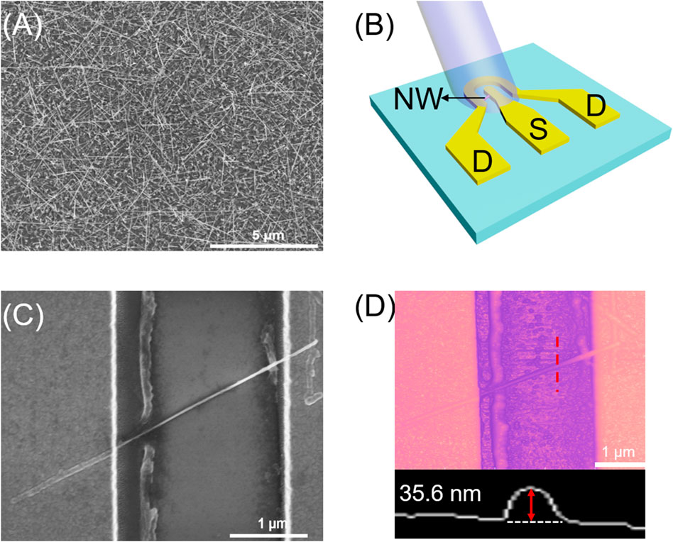
FIGURE 1. (A) SEM image of the as-grown InAs NWs to transfer. The scale bar is 5 μm; (B) 3D schematic diagram of the device structure; (C) SEM image and (D) AFM image of the as-fabricated InAs NW photodetector. The scale bar is 1 µm.
As shown in Figure 2A, typical I–V curves were obtained when the NW device was exposed to laser illumination at different wavelengths (405, 650, and 940 nm), at a power density of 500 mW/cm2. Different from the conventional photoconductive photodetectors, our test results reveal that the photocurrent will decrease sharply as laser irradiation is shed on the NW device. It can be clearly found that the response of the nanowire detector to light becomes weaker as the wavelength of light irradiation increases. For the InAs NW photodetector with a physical size far smaller than the wavelength of incidence, refraction of photons may lead to a weak light absorption. This effect would get severer as the wavelength of incidence gets longer, which is one of the main factors for low photoresponse to the infrared light [39, 40]. In addition, the surface electron accumulation layer has a great influence on carrier transport, resulting in a lower detectivity in the infrared regime as well [41–44]. Here, the Ilight is defined as the photocurrent under the illuminated state. The Idark is defined as the dark current, and the net photocurrent (IPC) is defined as IPC = | Ilight–Idark |. Figure 2B shows the dark current to photocurrent ratio as a function of bias voltage at different wavelengths. Under different wavelengths of incidence, the maximum dark current to photocurrent ratios are ∼130 (405 nm), ∼25 (650 nm), and ∼1.5 (940 nm).
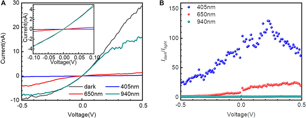
FIGURE 2. (A) I–V characteristics of the InAs NW photodetector device under 405 nm (blue), 650 nm (red), and 940 nm (dark green) illumination. The inset shows the zoom-in I–V curve swept from −0.1 to 0.1 V. The light intensity is 500 mW/cm2. (B) The dark current to photocurrent ratio as a function of bias voltage under laser incidence with different wavelengths.
To further understand the photoresponse characteristic of these NW detectors, the dependence of device photocurrent to the laser irradiation intensities (0.1, 50, 150, and 500 mW/cm2) is investigated and depicted in Figure 3A. For a typical photodetector with a positive photoresponse, the photoconductive gain (G), defined as the number of charges collected by the electrodes due to the excitation by one photon, can be expressed as [17]
where
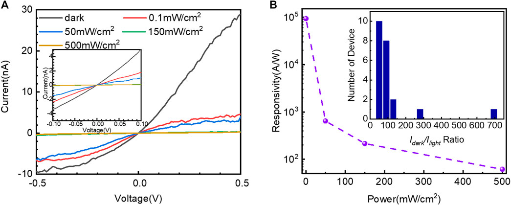
FIGURE 3. (A) I–V characteristics of the InAs NW photodetector under the 405 nm laser incidence at 0.1, 50, 150, and 500 mW/cm2. The inset shows the zoom-in I–V curve swept from −0.1 to 0.1 V. (B) Responsivity as a function of the incident illumination intensity. The inset shows the histogram of the maximum Idark/Ilight ratio of 22 InAs NW photodetectors.
The photoresponsivity (Rλ) is a very important parameter for a photodetector, which can be calculated as follows [28]:
where IPC is the net photocurrent and P is the light power absorbed by the NW. The responsivity of the device at a bias voltage of 0.5 V is shown in Figure 3B. The device exhibits a very large responsivity (closed to 105 A/W) when the light intensity is reduced to 0.1 mW/cm2, indicating a good sensitivity of the NW detector for weak signals. The inset shows the histogram distribution of the maximum Idark/Ilight ratio collected from 22 single InAs NW photodetectors. The devices all exhibit good negative photoelectric response, with the highest Idark/Ilight ratio of 700 being achieved.
The dynamic photoresponse is another important parameter to evaluate the performance of the detector. The time-resolved photoresponse of NW photodetectors is shown in Figure 4. The frequency of the modulation signal is set as 0.1 Hz, while the duty cycle is 50% and the light intensity is 150 mW/cm2. The detector can work stably after dozens of complete cycles. The rise and decay time constants, defined as the time interval for the current rise from 10 to 90% of the peak value and vice versa, representing the response and recovery time, are found to be 0.005 and 2.645 s, respectively, indicating the fast response and the slow recovery of the device. Different from the positive photoresponse, although the negative photoresponse exhibits a relatively fast photocurrent response process, the photocurrent recovery process is relatively slow. The slow recovery of photocurrent is believed to be caused by the increase in the dynamic relaxation time of carriers because of the traps in the light-induced gating layer. By fitting the light recovery current according to the following equation [32]:
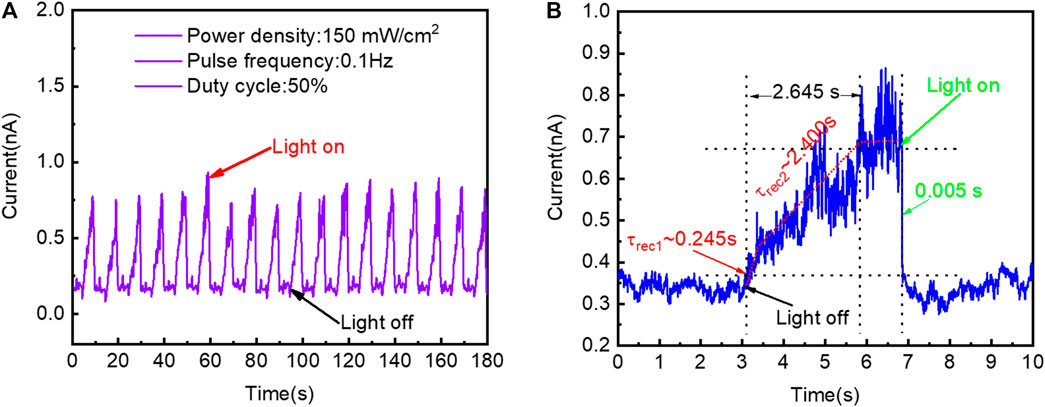
FIGURE 4. (A) Photoresponse of the NW photodetector under an illumination intensity of 150 mW/cm2. The chopped pulse frequency is 0.1 Hz, and the duty cycle is 50%. (B) A high-resolution transient photoresponse of the device to a pulse incidence.
To further explain the NPC effect, the chemical composition of the nanowires was first tested and analyzed using the high-resolution XPS, as shown in Figure 5. From the spectra, three sharp peaks at 40.63, 443.99, and 531.14 eV can be observed, representing the As3d, In3d, and O1s peaks, respectively. Furthermore, the In3d characteristic doublet peaks are shown in Figure 5C. The In3d 5/2 and In3d 3/2 binding energies appear at 443.9 and 451.4 eV, respectively. These observations have clearly shown the existence of the oxidization layer as the InAs NW exposed to the air. When there is no light, the free electrons in the NW core are driven by an external electric field to form a current, which is the so-called dark current. Due to the numerous defects, the Fermi level of the NW surface is pinned, leading to an energy bending in both conduction and valence bands. Acting as the PGL, the oxide layer would trap photogenerated carriers through the surface states, leading to a loss in the number of the carriers [29]. Additionally, it is worthy to note that surface scattering and recombination processes will also cause a degradation of the electron mobility close to the surface of the nanowire [45]. Meanwhile, as the incident power is very low, the photogenerated carriers would also recombine in the collection process, all contributing to a sharp decrease in the channel current. The NW size may play a role in the redistribution of carriers as well. [45, 46].
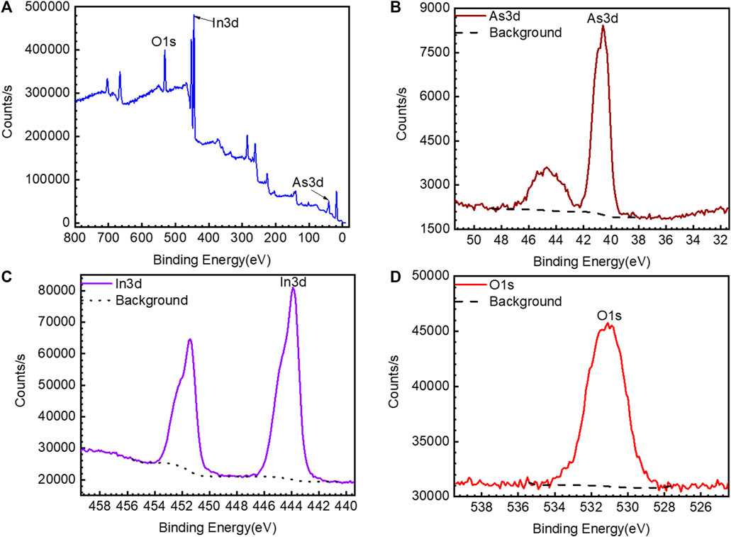
FIGURE 5. (A) High-resolution XPS spectra of InAs NWs. XPS spectra of (B) As3d and (C) In3d. (D) O1s for InAs NWs.
To conclude, InAs NWs have been grown on p-type silicon (111) wafers by MBE, and high-performance MSM photodetectors have been demonstrated. A high responsivity of approximately 105 A/W, an NPC gain of over 105, an Idark/Ilight ratio of more than 100, and a fast response time of less than 5 ms are obtained under normal temperature and pressure under 405 nm laser irradiation. Further analysis found that InAs nanowires are easily oxidized in the air, forming a gating layer, which can capture the photogenerated carriers in the nanowires. Moreover, this NW photodetector will pave a way to enable novel high-sensitivity broad-spectrum room-temperature detection.
The original contributions presented in the study are included in the article/Supplementary Material, and further inquiries can be directed to the corresponding authors.
YZ and DP conceived the idea and wrote part of the manuscript. XZ conducted the experiment and wrote the original version of the manuscript. XZ, YZ, and DP analyzed the results and prepared the figures. YZ proofread the manuscript. XY, JZ, and JL supervised the project. All authors have given approval to the final version of the manuscript.
The authors declare that the research was conducted in the absence of any commercial or financial relationships that could be construed as a potential conflict of interest.
All claims expressed in this article are solely those of the authors and do not necessarily represent those of their affiliated organizations or those of the publisher, the editors, and the reviewers. Any product that may be evaluated in this article, or claim that may be made by its manufacturer, is not guaranteed or endorsed by the publisher.
1. Dillen DC, Kim K, Liu E-S, Tutuc E. Radial Modulation Doping in Core-Shell Nanowires. Nat Nanotech (2014) 9:116–20. doi:10.1038/nnano.2013.301
2. Ju S, Facchetti A, Xuan Y, Liu J, Ishikawa F, Ye P, et al. Fabrication of Fully Transparent Nanowire Transistors for Transparent and Flexible Electronics. Nat Nanotech (2007) 2:378–84. doi:10.1038/nnano.2007.151
3. Gudiksen MS, Lauhon LJ, Wang J, Smith DC, Lieber CM. Growth of Nanowire Superlattice Structures for Nanoscale Photonics and Electronics. Nature (2002) 415(6872):617–20. doi:10.1038/415617a
4. Ford AC, Ho JC, Chueh Y-L, Tseng Y-C, Fan Z, Guo J, et al. Diameter-Dependent Electron Mobility of InAs Nanowires. Nano Lett (2009) 9(1):360–5. doi:10.1021/nl803154m
5. Kung S-C, van der Veer WE, Yang F, Donavan KC, Penner RM. 20 μs Photocurrent Response from Lithographically Patterned Nanocrystalline Cadmium Selenide Nanowires. Nano Lett (2010) 10(4):1481–5. doi:10.1021/nl100483v
6. Takahashi T, Takei K, Adabi E, Fan Z, Niknejad AM, Javey A. Parallel Array InAs Nanowire Transistors for Mechanically Bendable, Ultrahigh Frequency Electronics. Acs Nano (2010) 4(10):5855–60. doi:10.1021/nn1018329
7. Takei K, Takahashi T, Ho JC, Ko H, Gillies AG, Leu PW, et al. Nanowire Active-Matrix Circuitry for Low-Voltage Macroscale Artificial Skin. Nat Mater (2010) 9(10):821–6. doi:10.1038/nmat2835
8. Wallentin J, Anttu N, Asoli D, Huffman M, Aberg I, Magnusson MH, et al. InP Nanowire Array Solar Cells Achieving 13.8% Efficiency by Exceeding the Ray Optics Limit. Science (2013) 339(6123):1057–60. doi:10.1126/science.1230969
9. Han N, Wang F, Hou JJ, Yip SP, Lin H, Xiu F, et al. Tunable Electronic Transport Properties of Metal-Cluster-Decorated III-V Nanowire Transistors. Adv Mater (2013) 25(32):4445–51. doi:10.1002/adma.201301362
10. Saxena D, Mokkapati S, Parkinson P, Jiang N, Gao Q, Tan HH, et al. Optically Pumped Room-Temperature GaAs Nanowire Lasers. Nat Photon (2013) 7(12):963–8. doi:10.1038/nphoton.2013.303
11. Dayeh SA, Aplin DPR, Zhou X, Yu PKL, Yu ET, Wang D. High Electron Mobility InAs Nanowire Field-Effect Transistors. Small (2007) 3(2):326–32. doi:10.1002/smll.200600379
12. Dayeh SA. Electron Transport in Indium Arsenide Nanowires. Semicond Sci Technol (2010) 25(2):024004–24020. doi:10.1088/0268-1242/25/2/024004
13. Joyce HJ, Gao Q, Wong-Leung J, Kim Y, Tan HH, Jagadish C. Tailoring GaAs, InAs, and InGaAs Nanowires for Optoelectronic Device Applications. IEEE J Select Top Quan Electron. (2011) 17(4):766–78. doi:10.1109/JSTQE.2010.2077621
14. Joyce HJ, Gao Q, Hoe Tan H, Jagadish C, Kim Y, Zou J, et al. III-V Semiconductor Nanowires for Optoelectronic Device Applications. Prog Quan Elect (2011) 35(2-3):23–75. doi:10.1016/j.pquantelec.2011.03.002
15. Logeeswaran VJ, Oh J, Nayak AP, Katzenmeyer AM, Gilchrist KH, Grego S, et al. A Perspective on Nanowire Photodetectors: Current Status, Future Challenges, and Opportunities. IEEE J Sel Top Quan Electron (2011) 17(4):1002–32. doi:10.1109/JSTQE.2010.2093508
16. Das A, Ronen Y, Most Y, Oreg Y, Heiblum M, Shtrikman H. Zero-bias Peaks and Splitting in an Al-InAs Nanowire Topological Superconductor as a Signature of Majorana Fermions. Nat Phys (2012) 8(12):887–95. doi:10.1038/NPHYS2479
17. Miao J, Hu W, Guo N, Lu Z, Zou X, Liao L, et al. Single InAs Nanowire Room-Temperature Near-Infrared Photodetectors. ACS Nano (2014) 8(4):3628–35. doi:10.1021/nn500201g
18. Rota MB, Ameruddin AS, Fonseka HA, Gao Q, Mura F, Polimeni A, et al. Bandgap Energy of Wurtzite InAs Nanowires. Nano Lett (2016) 16(8):5197–203. doi:10.1021/acs.nanolett.6b02205
19. Lapierre RR, Robson M, Azizur-Rahman KM, Kuyanov P. A Review of III-V Nanowire Infrared Photodetectors and Sensors. J Phys D: Appl Phys (2017) 50(12):123001. doi:10.1088/1361-6463/aa5ab3
20. Dayeh SA, Soci C, Yu PKL, Yu ET, Wang D. Influence of Surface States on the Extraction of Transport Parameters from InAs Nanowire Field Effect Transistors. Appl Phys Lett (2007) 90(16):162112. doi:10.1063/1.2728762
21. Prins AD, Lewis MK, Bushell ZL, Sweeney SJ, Liu S, Zhang Y-H. Evidence for a Defect Level above the Conduction Band Edge of InAs/InAsSb Type-II Superlattices for Applications in Efficient Infrared Photodetectors. Appl Phys Lett (2015) 106(17):171111. doi:10.1063/1.4919549
22. Li B, Yan X, Zhang X, Luo Y, Lu Q, Ren X. Controllable Photoresponse Behavior in a Single InAs Nanowire Phototransistor. Appl Phys Lett (2017) 111(11):113102. doi:10.1063/1.4990597
23. Lynall D, Nair SV, Gutstein D, Shik A, Savelyev IG, Blumin M, et al. Surface State Dynamics Dictating Transport in InAs Nanowires. Nano Lett (2018) 18(2):1387–95. doi:10.1021/acs.nanolett.7b05106
24. Shen L, Yip S, Lan C, Shu L, Li D, Zhou Z, et al. Enhanced Negative Photoconductivity in InAs Nanowire Phototransistors Surface-Modified with Molecular Monolayers. Adv Mater Inter (2018) 5(3):1701104. doi:10.1002/admi.201701104
25. Zhang X, Yao X, Li Z, Zhou C, Yuan X, Tang Z, et al. Surface-States-Modulated High-Performance InAs Nanowire Phototransistor. J Phys Chem Lett (2020) 11(15):6413–9. doi:10.1021/acs.jpclett.0c01879
26. Halpern E, Elias G, Kretinin AV, Shtrikman H, Rosenwaks Y. Direct Measurement of Surface States Density and Energy Distribution in Individual InAs Nanowires. Appl Phys Lett (2012) 100(26):262105. doi:10.1063/1.4731211
27. Fang H, Hu W, Wang P, Guo N, Luo W, Zheng D, et al. Visible Light-Assisted High-Performance Mid-infrared Photodetectors Based on Single InAs Nanowire. Nano Lett (2016) 16(10):6416–24. doi:10.1021/acs.nanolett.6b02860
28. Liu Z, Luo T, Liang B, Chen G, Yu G, Xie X, et al. High-detectivity InAs Nanowire Photodetectors with Spectral Response from Ultraviolet to Near-Infrared. Nano Res (2013) 6(11):775–83. doi:10.1007/s12274-013-0356-0
29. Guo N, Hu W, Liao L, Yip S, Ho JC, Miao J, et al. Anomalous and Highly Efficient InAs Nanowire Phototransistors Based on Majority Carrier Transport at Room Temperature. Adv Mater (2014) 26(48):8203–9. doi:10.1002/adma.20147032910.1002/adma.201403664
30. Yang Y, Peng X, Kim H-S, Kim T, Jeon S, Kang HK, et al. Hot Carrier Trapping Induced Negative Photoconductance in InAs Nanowires toward Novel Nonvolatile Memory. Nano Lett (2015) 15(9):5875–82. doi:10.1021/acs.nanolett.5b01962
31. Han Y, Zheng X, Fu M, Pan D, Li X, Guo Y, et al. Negative Photoconductivity of InAs Nanowires. Phys Chem Chem Phys (2016) 18(2):818–26. doi:10.1039/c5cp06139c
32. Han Y, Fu M, Tang Z, Zheng X, Ji X, Wang X, et al. Switching from Negative to Positive Photoconductivity toward Intrinsic Photoelectric Response in InAs Nanowire. ACS Appl Mater Inter (2017) 9(3):2867–74. doi:10.1021/acsami.6b13775
33. Zhou J, Gu Y, Hu Y, Mai W, Yeh P-H, Bao G, et al. Gigantic Enhancement in Response and Reset Time of ZnO UV Nanosensor by Utilizing Schottky Contact and Surface Functionalization. Appl Phys Lett (2009) 94(19):191103. doi:10.1063/1.3133358
34. Chen M-W, Chen C-Y, Lien D-H, Ding Y, He J-H. Photoconductive Enhancement of Single ZnO Nanowire through Localized Schottky Effects. Opt Express (2010) 18(14):14836–41. doi:10.1364/OE.18.014836
35. Lind E, Persson AI, Samuelson L, Wernersson L-E. Improved Subthreshold Slope in an InAs Nanowire Heterostructure Field-Effect Transistor. Nano Lett (2006) 6(9):1842–6. doi:10.1021/nl052468b
36. Miao J, Hu W, Guo N, Lu Z, Liu X, Liao L, et al. High-Responsivity Graphene/InAs Nanowire Heterojunction Near-Infrared Photodetectors with Distinct Photocurrent On/Off Ratios. Small (2015) 11(8):936–42. doi:10.1002/smll.201402312
37. Zhang X, Huang H, Yao X, Li Z, Zhou C, Zhang X, et al. Ultrasensitive Mid-wavelength Infrared Photodetection Based on a Single InAs Nanowire. ACS Nano (2019) 13:3492–9. doi:10.1021/acsnano.8b09649
38. Pan D, Fu M, Yu X, Wang X, Zhu L, Nie S, et al. Controlled Synthesis of Phase-Pure InAs Nanowires on Si(111) by Diminishing the Diameter to 10 nm. Nano Lett (2014) 14(3):1214–20. doi:10.1021/nl4040847
39. Hang Q, Wang F, Carpenter PD, Zemlyanov D, Zakharov D, Stach EA, et al. Role of Molecular Surface Passivation in Electrical Transport Properties of InAs Nanowires. Nano Lett (2008) 8(1):49–55. doi:10.1021/nl071888t
40. Du J, Liang D, Tang H, Gao XPA. InAs Nanowire Transistors as Gas Sensor and the Response Mechanism. Nano Lett (2009) 9(12):4348–51. doi:10.1021/nl902611f
41. Olsson LÖ, Andersson CBM, Håkansson MC, Kanski J, Ilver L, Karlsson UO. Charge Accumulation at InAs Surfaces. Phys Rev Lett (1996) 76(19):3626–9. doi:10.1103/PhysRevLett.76.3626
42. Weber JR, Janotti A, Van de Walle CG. Intrinsic and Extrinsic Causes of Electron Accumulation Layers on InAs Surfaces. Appl Phys Lett (2010) 97(19):192106. doi:10.1063/1.3518061
43. Noguchi M, Hirakawa K, Ikoma T. Intrinsic Electron Accumulation Layers on Reconstructed Clean InAs(100) Surfaces. Phys Rev Lett (1991) 66(17):2243–6. doi:10.1103/PhysRevLett.66.2243
44. Ichikawa S, Sanada N, Mochizuki S, Esaki Y, Fukuda Y, Shimomura M, et al. Structure of anInAs(111)A−(2×2)Ssurface Studied by Scanning Tunneling Microscopy, Photoelectron Spectroscopy, and X-ray Photoelectron Diffraction. Phys Rev B (2000) 61(19):12982–7. doi:10.1103/PhysRevB.61.12982
45. Li J, Yan X, Sun F, Zhang X, Ren X. Anomalous Photoconductive Behavior of a Single InAs Nanowire Photodetector. Appl Phys Lett (2015) 107(26):263103. doi:10.1063/1.4938752
Keywords: InAs, nanowires, negative photoconductivity, photodetector, wide-spectrum
Citation: Zhang X, Zhang Y, Pan D, Yi X, Zhao J and Li J (2021) Negative Photoconductive Effects in Uncooled InAs Nanowire Photodetectors. Front. Phys. 9:725680. doi: 10.3389/fphy.2021.725680
Received: 15 June 2021; Accepted: 13 September 2021;
Published: 21 October 2021.
Edited by:
Jun Wang, University of Electronic Science and Technology of China, ChinaReviewed by:
Yaping Dan, Shanghai Jiao Tong University, ChinaCopyright © 2021 Zhang, Zhang, Pan, Yi, Zhao and Li. This is an open-access article distributed under the terms of the Creative Commons Attribution License (CC BY). The use, distribution or reproduction in other forums is permitted, provided the original author(s) and the copyright owner(s) are credited and that the original publication in this journal is cited, in accordance with accepted academic practice. No use, distribution or reproduction is permitted which does not comply with these terms.
*Correspondence: Yiyun Zhang, eXl6aGFuZ0BzZW1pLmFjLmNu; Dong Pan, cGFuZG9uZ0BzZW1pLmFjLmNu
Disclaimer: All claims expressed in this article are solely those of the authors and do not necessarily represent those of their affiliated organizations, or those of the publisher, the editors and the reviewers. Any product that may be evaluated in this article or claim that may be made by its manufacturer is not guaranteed or endorsed by the publisher.
Research integrity at Frontiers
Learn more about the work of our research integrity team to safeguard the quality of each article we publish.