
94% of researchers rate our articles as excellent or good
Learn more about the work of our research integrity team to safeguard the quality of each article we publish.
Find out more
ORIGINAL RESEARCH article
Front. Phys., 27 July 2021
Sec. Optics and Photonics
Volume 9 - 2021 | https://doi.org/10.3389/fphy.2021.710092
 Ryoya Hiramatsu1Ryo Takahashi1Ryoto Fujiki1Keisuke Hozo1Kanato Sawai1
 Dong-Pyo Han1*
 Motoaki Iwaya1Tetsuya Takeuchi1Satoshi Kamiyama1Isamu Akasaki1,2
In this paper, a hybrid numerical simulation tool is introduced and performed for GaInN-based light-emitting diodes (LEDs) with metal-embedded nanostructure to theoretically predict external quantum efficiency (EQE), which composed of finite-difference time-domain, rigorous coupled wave analysis, and ray tracing. The advantage is that the proposed method provides results supported by sufficient physical background within a reasonable calculation time. From the simulation results, the EQE of LED with Ag-nanoparticles embedded nanostructure is expected to be enhanced by as high as ∼1.6 times the conventional LED device in theory.
III-nitride semiconductor devices are the most promising devices for next-generation optoelectronics owing to their intrinsic natures of direct and wide bandgaps operating in the visible and ultraviolet (UV) spectral regions [1, 2]. Examples of III-nitride optoelectronic devices include photodiodes, solar cells, laser diodes, and light-emitting diodes (LEDs). Most notably, significant progress has been made in the research and development of high-efficiency GaInN-based LEDs since the first demonstration of high-quality and p-type GaN films on a sapphire substrate by Akasaki et al. This achievement is hailed as one of the greatest accomplishments in modern semiconductor technology [3, 4]. Thanks to these efforts, GaInN-based LEDs have now been widely adopted as a dominant high-brightness emitter in the spectral range from green to near-UV for various applications. Furthermore, general white lighting can be realized by utilizing a blue LED and yellow phosphor. The replacement of conventional lighting sources with LEDs can provide huge benefits such as energy savings, increased lifetime span, and environmental friendliness [5].
Although the performance of LED devices has significantly improved to date, higher light output power and lower electrical power consumption, i.e., higher external quantum efficiency (EQE, ηEQE), are still required for further energy savings. In theory, the EQE of LED devices is expressed as the product of two element efficiencies, i.e., light extraction efficiency (LEE, ηLEE) and internal quantum efficiency (IQE, ηIQE): EQE = LEE × IQE [6, 7]. This implies two distinct strategies to improve LED devices, i.e., improve either LEE or IQE. It is noteworthy that the LEE and IQE are defined as [(the number (#) of photons escaped to free space per second)/(# of photons generated in the active region per second)] and [(# of photons generated in the active region per second)/(# of carriers injected into the active region per second)], respectively [7].
In GaInN-based LEDs, the escape cone of photons from inside the semiconductor to free space is as narrow as ∼25° due to the large difference in refractive index (n) between GaN and air (nGaN ∼ 2.5 and nair ∼ 1). This results in an escape probability that is lower than ∼5% from the top surface of LEDs, and the rest of the photons are trapped inside and dissipated as heat [8, 9]. In short, the LEE of GaInN-based LEDs is inherently very low. For that reason, several structures, e.g., patterned sapphire substrates (PSSs), surface texturing, air-void, flip-chip, and sidewall roughening [10–14], have been introduced and widely adopted in commercial LED devices to improve the LEE of GaInN-based LEDs. It is noteworthy that the abovementioned structures were designed to improve the LEE through the reduction of total internal reflection (TIR). More recently, GaInN-based LEDs employing nanostructures have been studied in depth to improve the LEE, e.g., nano-PSSs (nPSSs), photonic crystals, metal nanoparticles on a device surface, and periodical nanohole patterning [15–19]. The size of the nanostructure is typically comparable to or smaller than the emission wavelength of the LED. In contrast to the conventional structure, LEDs with nanostructures were also designed to improve the LEE through not only the reduction of the TIR, but also the cavity effect at a resonant frequency [19, 20]. In other words, suppression of the guide mode inside device and enhancement of the leaky mode to free space are expected simultaneously. In this context, a nanostructure should be designed very carefully to take advantage of both TIR and guide mode suppression to improve the LEE.
Aside from issues related to the LEE, the IQE of GaInN-based LEDs still suffers from well-known “green-gap” issue. The IQE of green LEDs at a usual operating current is lower than ∼30% and decreases further as the driving current and/or emission wavelength increases [6, 7]. To improve the IQE, tremendous efforts have been made in epitaxial growth and device fabrication. Of which, surface-plasmon (SP)-enhanced LEDs have attracted great attention and have been intensively studied because SP-mode works very efficiently in GaInN-based green LEDs [21–24]. In particular, LEDs with metal-nanoparticle (NP)-embedded nanostructures have demonstrated great IQE improvement. Specifically, additional recombination channels are created by metal-NPs in LEDs via exciton coupling with localized SP (LSP) modes, which effectively decrease the carrier density in the active region and the radiative carrier lifetimes. Consequently, the IQE is enhanced [25–27]. In principle, SP and LSP modes are expected to be most active at the SP/LSP resonant frequency of the metal-NPs, i.e., when the frequency of the emitted photon overlaps the SP resonant frequency. Therefore, the design and shape of metal-embedded nanostructures are crucially important to improve the IQE because the resonant frequency of the SP mode strongly depends on the type, design, and shape of the metal-NPs.
Collectively, an LED with metal-embedded nanostructures is believed to have great potential to improve the EQE because simultaneous improvement of the LEE and IQE is expected. In other words, the metal-embedded nanostructure should be designed and optimized so that both effects work well simultaneously. From this viewpoint, numerical simulation is a very useful tool for designing a structure as it enables the theoretical prediction of the efficiencies while considering both effects. However, in spite of the significant importance of numerical calculations in nanostructure design, there are still no suitable simulation tools covering both the LEE and the SP effect due to their complex structure and calculation. For example, the ray tracing (RT) method, which is the most widely used method for LEE calculation in LEDs, does not consider the wave characteristics of light and the SP/LSP effect. Therefore, results from this method may be inaccurate when the size of the nanostructure is close to the emission wavelength. Hence, the RT method is typically limited to the LED employing microstructure, despite advantages such as short calculation time and scalability to large computational domains. Meanwhile, the finite-difference time-domain (FDTD) method is often adopted to calculate the SP effect in LEDs, but this method is only suitable for calculating one specific nanostructure. That is, it is unreasonable to practically use the FDTD method because it takes an enormous amount of time to expand and apply it to an entire LED structure [28]. Hence, the FDTD method is typically limited to the computational domains of a few micrometers, despite of advantages such as accuracy, considering the nature of the wave, and the dispersion relation. From a practical point of view, an adequate numerical simulation tool for SP-enhanced LEDs with metal-NP-embedded nanostructures is required for optimizing design via numerical calculation and theoretical prediction.
In this paper, a hybrid numerical simulation tool is introduced and performed for GaInN-based LEDs with metal-NP-embedded nanostructures to theoretically predict EQE improvement via design optimization. The proposed tool combines three types of simulation methods: FDTD [29], rigorous coupled wave analysis (RCWA) [30], and RT [31]. Importantly, the advantage of the proposed hybrid method is that both natures of light, i.e., wave and ray properties, are flexibly taken into the numerical calculation, depending on the method, within a reasonable calculation time. Another important advantage is computation time. Specifically, the RCWA method can provide the huge merit in terms of calculation time and computing power for periodically patterned structure. Namely, it can greatly simplify the problem of periodic patterns since this method solves the problem in the Fourier space. Using the hybrid simulation method proposed in this study, we demonstrate the optimized structure of LEDs with metal-embedded nanostructures, i.e., a design in which the EQE is maximized. In addition, from the perspective of practical usage, the calculation time of the proposed method is compared to the case of the FDTD simulation for the entire structure.
Figure 1A displays a schematic of the LED structure under investigation in this study. The structure is simple, composed of four layers that include a sapphire substrate (t = 100 μm), an n-GaN layer (t = 5 μm), a multiple-quantum-wells (MQWs) active layer (t = 100 nm), and a p-GaN layer (t = 120 nm). The sample size is 300 × 300 μm2 with an emission wavelength of 520 nm. The p-GaN surface contains periodically etched nanoscale-hole patterns that are cylindrical and filled with Ag-NPs. Note that a flat sapphire substrate is employed in this study to intensively investigate the effect of the Ag-embedded nanostructures in the p-GaN surface on the EQE. X, Y, and Z in Figure 1A represent the diameter of a single hole-pattern, the pitch between two hole-patterns, and the etch depth, respectively. As an attempt to optimize the structure, we varied X and Y while Z was fixed at 50 nm because of the limitation of junction depletion (the depletion region toward the p-GaN is ∼70 nm in typical GaInN-based LEDs) [32]. Figure 2B displays a flowchart of the hybrid simulation performed in this study. First, the E-field energy densities enhanced by the SP/LSP mode were calculated via the FDTD method for single and dual Ag-embedded nanostructures. The FDTD was performed repeatedly with varying X and Y to optimize the nanostructure. Next, the dispersion characteristics of the p-GaN surface, including the reflectance (R) and transmittance (T) from the periodic pattern array, were calculated by the RCWA method for a single unit cell of an Ag-embedded nanostructure. The RCWA method was also performed repeatedly with varying Y to optimize. Then, the RT method was performed using the data obtained from the RCWA to theoretically predict LEE enhancement from the periodic nanostructure. Lastly, taking into account both the IQE from the FDTD and the LEE from the RT, an optimized structure is proposed, that is, the Ag-embedded nanostructure with the highest EQE. Most notably, the hybrid method takes less than 1% of the calculation time required for an entire LED structure via the FDTD method, i.e., it saves a huge amount of calculation time and computing power. This is because the RCWA method adopts a Fourier space method, which can simplify the periodic structure problem. All simulation parameters used in this study are listed in Table 1.
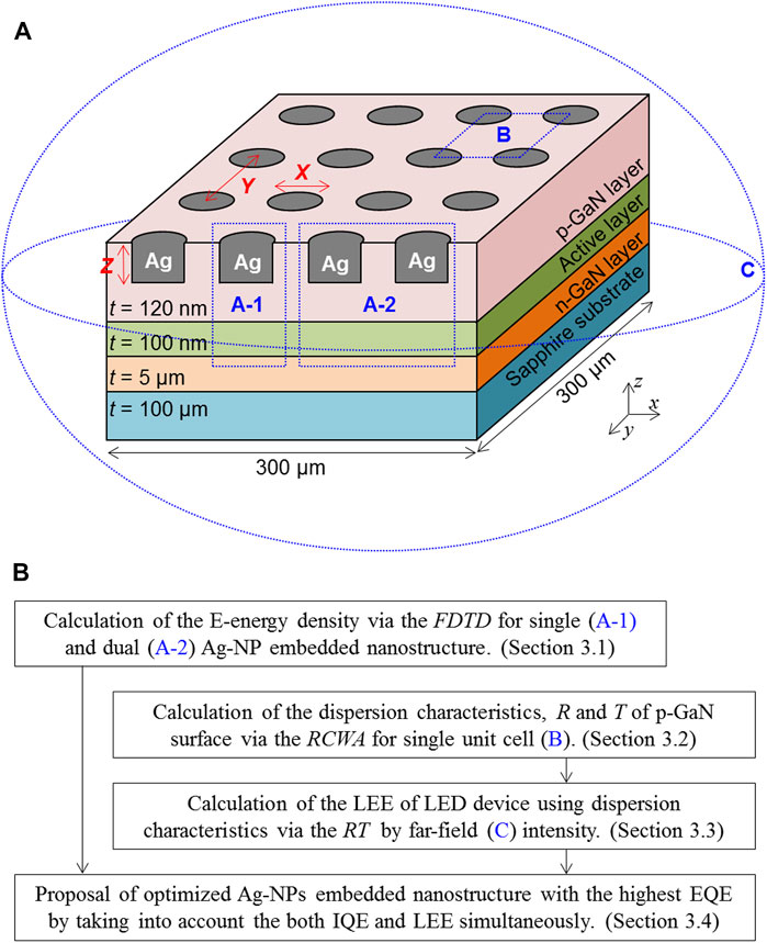
FIGURE 1. (A) Schematic of the LED structure under investigation and (B) a flowchart of the three-method hybrid simulation proposed in this study.
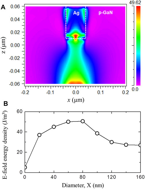
FIGURE 2. (A) E-field energy distribution on the x–z plane for a single nanostructure with X = 80 nm and (B) peak values of the E-field energy density at the bottom of the Ag-NPs as a function of X.
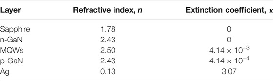
TABLE 1. Summary of the simulation parameters used in this study.
In this section, we systematically investigated the effect of the nanostructure parameters, such as the diameter of a single hole-pattern (X in Figure 1A) and the pitch between two hole-patterns (Y in Figure 1A), on the IQE via the E-field energy density distribution. For the FDTD simulation in this work, a commercial FDTD simulation program was used [29] wherein perfectly matched layer boundary conditions were employed on all boundaries of the domain. The spatial cell size of the calculation domain was 5 nm for all dx, dy, and dz. A single dipole source was placed at the center of the MQW active region in the x-direction of Figure 1A. The dipole source was assumed to emit a wavelength of 520 nm. In GaN material systems, Ag thin film is typically used as surface plasmonic source. This is because the resonance frequency of the surface-plasmon theoretically corresponds to visible wavelength, i.e., Ag/GaN is ∼2.8 eV (∼442 nm). When the frequency of emitted photon matches to the resonance frequencies of the surface-plasmon, the radiative recombination process of LED is enhanced, resulting in the IQE improvement. Notably, the resonance frequency of Ag/GaN is dependent of the size, i.e., red-shift when the size of metal decreases. Therefore, it is important to investigate the size of Ag to match the resonant frequency of the surface-plasmon with the frequency of the emitted photons. First, to investigate the effect of hole-pattern diameter, single nanostructures were first simulated by the FDTD, i.e., A-1 in Figure 1A was contained inside the computational domain with varying X. Figure 2A shows the steady-state E-field energy distribution on the x–z plane for a single nanostructure with X = 80 nm. It is clearly observed that the bottom of the Ag-NPs is oscillated with the EM-field from the dipole source. This indicates that an additional recombination channel was created through exciton coupling with the SP/LSP mode [33]. In Figure 2B, the peak values of the E-field energy density at the bottom of the Ag-NPs, i.e., the oscillated intensity by the EM-field of the dipole source, are plotted as a function of X. As shown in Figure 2B, the strongest E-field energy density was observed at X = 80 nm, implying that the SP/LSP mode of the Ag-NPs was most activated by the emission source of 520 nm when X is ∼80 nm. This is because the resonant frequency of the SP/LSP mode depends on the shape and size of the NPs and the type of metal [22]. Consequently, from the result in Figure 2B, the IQE is expected to be most enhanced by the SP/LSP mode of Ag-NPs with a diameter of 80 nm. Next, to investigate the effect of the laterally coupled oscillation of NPs, i.e., surface-plasmon polariton (SPP) propagation [34], on IQE enhancement, a dual nanostructure array was simulated by FDTD, i.e., A-2 in Figure 1A was contained inside the computational domain with varying Y and with X fixed at 80 nm. Figure 3A shows the steady-state E-field energy distribution on the x–z plane for the dual nanostructure with X = 80 nm and Y = 294 nm. Apparently, SPP propagation was observed at the sidewall of the Ag-NPs. It is noteworthy that a greater E-field energy than that of a single structure was obtained and believed to be owing to SPP resonance. In Figure 3B, the peak values of the E-field energy density at the sidewall of the Ag-NPs are plotted as a function of Y. Somewhat surprisingly, two singularities were obtained at Y = 187 and 294 nm in Figure 3B. This result means that the SPP propagation resonates by meeting the criteria. According to the dispersion relation, an emission wavelength (λ) of ∼520 nm effectively diminishes to ∼0.6λ in the GaN material [17]. At two singularities, the distances between the Ag-NP sidewalls are ∼0.3λ for Y = 187 nm and ∼0.6λ for Y = 294 nm, indicating that the criterion is the constructive interference of the SPP mode, i.e., the lattice resonance. Thus, we can infer that the two singularities in Figure 3B are caused by meeting the criteria, i.e., the resonance cavity effect of SPPs. Consequently, the IQE is expected to be enhanced most by the SP/LSP mode with nanostructure parameters of X = 80 nm and Y = 187 nm or X = 80 nm and Y = 294 nm.
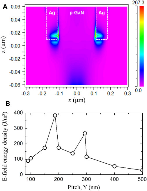
FIGURE 3. (A) E-field energy distribution on the x–z plane for the dual nanostructure with X = 80 nm and Y = 294 nm and (B) peak values of the E-field energy density at the sidewall of Ag-NPs as a function of Y.
In this section, to investigate the effect of the nanostructure periodic array on device performance, the RCWA method was performed for a single unit cell of a nanostructure array. Figure 4A shows the configuration of the single unit cell used for the RCWA simulation, which was repeatedly performed with varying Y. The RCWA method is typically employed to solve an EM-field in a given periodic structure wherein the devices and fields are represented by a sum of spatial harmonics. In other words, the RCWA solves the problems in a Fourier space. In short, this method can provide huge advantages in terms of calculation time because it enables simplification of the problem for a periodic structure [30]. Figures 4B,C show the calculation results of the dispersion characteristics, namely, T and R as a function of the incident angle from the normal direction (0°) to the primary plane (90°) depending on the pitch, Y. As shown in Figures 4A,B, the critical angle of the escape cone seems to be independent of Y (∼28°), whereas T and R are dependent of Y, i.e., the T around the normal direction increases and the R around 45° increases with increasing Y. This result implies that the far field distribution and intesity of an emitted photon can be varied with Y. Consequently, the escape probability of photons from the p-GaN surface to free space is significantly affected by the nanostructure arrangement.
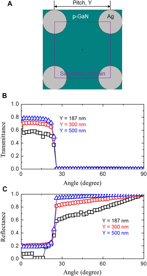
FIGURE 4. (A) Schematic of a unit cell on the x–y plane for the RCWA simulation and calculation results of (B) transmittance and (C) reflectance as a function of the incident angle from the normal direction (0°) to the primary plane (90°) depending on the pitch, Y.
In the previous section, the dispersion characteristics of the p-GaN surface due to a periodical nanostructure array, such as the angle distribution of R and T, were obtained. In this section, the LEEs of an LED with Ag-NP-embedded nanostructures are calculated by the RT method using data from the dispersion characteristics. To incorporate the effect of a periodical nanostructure array on the RT simulation, the dispersion characteristics from the RCWA method were referenced at the p-GaN surface of the LED instead of a simple n. In detail, when the rays reach the p-GaN surface, the data of the angle distribution of the R and T from the RCWA method are taken into account [28]. A configuration of the RT is shown in Figure 5A, and 500,000 rays were simulated in random directions from the MQWs. Then, the far field intensity was compared to obtain the LEE. This is an especially useful approach to obtain the LEEs of an LED with a periodical nanostructure array as both natures of light, i.e., wave and ray properties, are considered in the RT method and calculation time is saved. That is, the method in this section provides results supported by sufficient physical background within a reasonable calculation time. Figures 5B,C are the simulation results of the far-field angle distribution of luminescence for two cases: the LED with the pitch distance between Ag-NPs of 2) 400 nm and 3) 187 nm, respectively. In the results, the up side (0°) depicts the emission from the p-GaN surface and the down side (180°) depicts the emission from the sapphire surface, respectively. Here, we compared the two samples with the pitch distance of 400 and 187 nm, because a lattice plasmon resonance is expect for pitch distance of 187 nm and a typical characteristic is expected for pitch distance of 400 nm (see Figure 3A). As expected, Figure 5B shows typical Lambertian-like characteristics of far-field distribution. On the other hand, Figure 5C shows the notable difference from Figure 5B: 1) the luminescence is significantly enhanced at emission angle of 30° and 330°, and 2) the ratio of emission from p-GaN to that from the sapphire surface is greatly enhanced. Therefore, the result in Figure 5C suggests that the mode emission, most likely leaky mode, is enhanced by the lattice plasmon resonance, resulting in such different far-field characteristic. Note that, when the pitch is 187 nm, the area occupied by Ag-NPs in p-GaN surface is larger than the one for 400 nm, resulting in overall lower emission intensity and LEE. Figure 5D exhibits the LEE as a function of pitch, Y. The LEEs gradually increase as the pitch distance increases. Note that the singularities, as shown Figure 3B, are not shown in this result even at Y = 187 and 294 nm. The result of the LEEs in Figure 5D is in line with the result in Figures 4B,C because the T increases and the R decreases with increasing Y around the normal direction. For ray escape probability, the emission area of the p-GaN surface decreases with decreasing Y, i.e., the area occupied by Ag-NPs increases. This could be another cause of the result in Figure 5D.
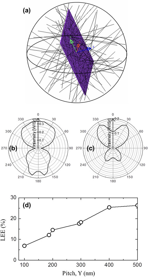
FIGURE 5. (A) Configuration of the ray tracing simulation, and calculation results of far-field angle distribution of luminescence for the LED with the pitch distance between Ag-NPs of (B) 400 nm and (C) 187 nm, and (D) LEEs plotted as a function of the pitch, Y.
Typically, the EQE of conventional LEDs without the SP/LSP mode is given by
where RR and RNR are the radiative and nonradiative recombination rates, respectively. Meanwhile, the EQE of SP/LSP-enhanced LEDs is given by [22].
where RSPC and Cext are the SP coupling rate and the probability of photon extraction from the SP energy, respectively. Eq. 2 indicates that the EQE is enhanced by the additional recombination channel (RSPC × Cext), that is, exciton coupling with the SP/LSP mode enhances the radiative recombination rate. In other words, the IQE is enhanced because an overlap of the local EM-field (see Figures 2, 3) increases both the SP coupling rate (RSPC) and the probability of photon extraction from the SP energy (Cext) [21, 33]. Here, the IQE enhanced by the SP/LSP mode can be estimated using the results in Figure 3B. To this end, we assumed that the conventional IQE is 30% and RSPC × Cext is proportional to the result in Figure 3B. Using Eq. 2 and the previously mentioned assumptions, the IQE can be estimated approximately, which is plotted as a function of Y in Figure 6A. As expected, the IQE is most enhanced by the SP/LSP modes at Y = 187 and 294 nm. Since IQE and LEE were obtained in Figure 5D and Figure 6A, we can plot the EQE as a function of Y, which is shown in Figure 6B. We can see that the EQE is most enhanced at Y = 294 nm. Briefly, X = 80 nm and Y = 294 nm are the optimized parameters for an Ag-NP-embedded nanostructure. Note that the overall EQE is low because a flat sapphire substrate is employed in this study. Consequently, the EQE of an LED device with an Ag-NP-embedded nanostructure is expected to be enhanced by as much as ∼1.6 times a conventional LED device in theory (where the IQE and the LEE are 30 and 22% for a conventional LED, respectively). The IQE improvement of ∼30% by SP/LSP mode has been theoretically predicted and experimentally demonstrated in our previous paper [21, 22]. Also, the LEE improvement of ∼22% by nanostructure (or photonic crystal) has been experimentally demonstrated in previous papers [8, 15]. Thus, we firmly believe that the simulation results given in this study are reasonable. Notably, to the best our knowledge, this is the first time that the reasonable EQE improvement is simulated in a short time using the hybrid method.
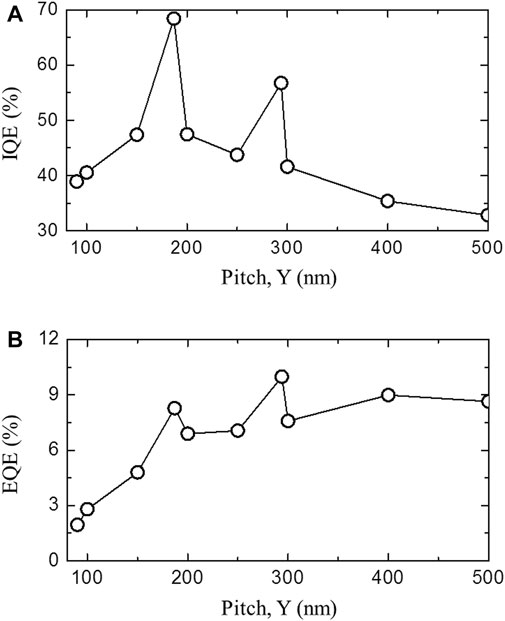
FIGURE 6. Calculation results of the (A) IQEs and (B) EQEs of the LED device plotted as a function of the pitch, Y.
In summary, a hybrid simulation composed of FDTD, RCWA, and RT was introduced and performed for an LED with an Ag-NP-embedded nanostructure. First, the FDTD was performed for single and dual nanostructures to optimize the diameter, X, and the pitch, Y, of the nanostructure. From the FDTD simulation results, the SP/LSP mode, which enhances the IQE of an LED, was confirmed, and optimized nanostructure parameters (X = 80 nm and Y = 187 nm, or X = 80 nm and Y = 294 nm) were proposed. Next, the RCWA method was performed for a single unit cell of the nanostructure array to investigate the effect of the periodic nanostructure array on the LEE. From the RCWA simulation, the dispersion characteristics, such as the T and R dependence on the incident angle of the p-GaN surface, were obtained. Then, the LEEs of an LED with an Ag-NP-embedded nanostructure were calculated by the RT method using data from the dispersion characteristics. The results showed that the LEEs gradually increase as the pitch distance increases. Lastly, considering both the IQE from the FDTD and the LEE from the RT, an optimized structure was proposed. Importantly, the advantage of the proposed hybrid method is that the results are supported with sufficient physical background and require a reasonable calculation time. It should be noted that the proposed method in this study is taken with only 1% of the calculation time compared to the case of the conventional FDTD simulation for the entire structure, which means the great advantages in practical use and computing power. In this paper, only simulation results were discussed, but we will fabricate an LED with Ag-NP-embedded nanostructures on the basis of the nanostructure parameters proposed in this study. It is believed that one can discuss the accuracy of proposed hybrid simulation in this study and demonstrate the increase in EQE of GaInN-based green LEDs in the near future.
The raw data supporting the conclusions of this article will be made available by the authors, without undue reservation.
RH wrote the manuscript, analyzed data, and performed simulations under supervising of D-PH revised the manuscript. RT, RF, KH, and KS contributed to the discussions. MI, TT, SK, and IA led the project and supervised the work.
This work was supported by MEXT Private University Research Branding Project, MEXT Program for research and development of next-generation semiconductor to realize energy-saving society, JSPS KAKENHI for Scientific Research A (No. 15H02019), JSPS KAKENHI for Scientific Research A (No. 17H01055), JSPS KAKENHI for Innovative Areas (No. 16H06416), and Japan Science and Technology CREST (No. 16815710).
The authors declare that the research was conducted in the absence of any commercial or financial relationships that could be construed as a potential conflict of interest.
All claims expressed in this article are solely those of the authors and do not necessarily represent those of their affiliated organizations, or those of the publisher, the editors and the reviewers. Any product that may be evaluated in this article, or claim that may be made by its manufacturer, is not guaranteed or endorsed by the publisher.
The authors would like to thank Mizuki Terazawa at E&E EVOLUTION Co., Japan for the technical supports and the assistance for the simulation.
1. Amano H. In: T-Y Seong, J Han, H Amano, and H Morkoç, editors. III-nitride Based Light Emitting Diodes and Applications. Heidelberg: Springer (2013). Chapter 1.
2. Schubert EF. Light-Emitting Diodes. 2nd ed. New York: Cambridge University Press (2006). Chapter 1. doi:10.1017/cbo9780511790546
3. Akasaki I. Nobel Lecture: Fascinated Journeys into Blue Light. Rev Mod Phys (2015) 87:1119–31. doi:10.1103/revmodphys.87.1119
4. Akasaki I, Amano H. Crystal Growth and Conductivity Control of Group III Nitride Semiconductors and Their Application to Short Wavelength Light Emitters. Jpn J Appl Phys (1997) 36:5393–408. doi:10.1143/jjap.36.5393
5. Akasaki I, Amano H. Breakthroughs in Improving Crystal Quality of GaN and Invention of the P-N Junction Blue-Light-Emitting Diode. Jpn J Appl Phys (2006) 45:9001–10. doi:10.1143/jjap.45.9001
6. Han DP, Yamanoto K, Ishimoto S, Iwaya M, Takeuchi T, Kamiyama S, et al. Determination of Internal Quantum Efficiency in GaInN-Based Light-Emitting Diode under Electrical Injection: Carrier Recombination Dynamics Analysis. Appl Phys Express (2019) 12:032006. doi:10.7567/1882-0786/aafca2
7. Han D-P, Shin D-S, Shim J-I, Kamiyama S, Takeuchi T, Iwaya M, et al. Modified Shockley Equation for GaInN-Based Light-Emitting Diodes: Origin of the Power- Efficiency Degradation under High Current Injection. IEEE J Quan Electron. (2019) 55:1–11. doi:10.1109/jqe.2019.2917180
8. Ee Y-K, Kumnorkaew P, Arif RA, Tong H, Tong H, Gilchrist JF, et al. Light Extraction Efficiency Enhancement of InGaN Quantum wells Light-Emitting Diodes with Polydimethylsiloxane Concave Microstructures. Opt Express (2009) 17:13747–57. doi:10.1364/oe.17.013747
9. Han D-P, Shim J-I, Shin D-S. Carrier Accumulation in the Active Region and its Impact on the Device Performance of InGaN-Based Light-Emitting Diodes. Appl Phys Express (2017) 10:122101. doi:10.7567/apex.10.122101
10. Yamada M, Mitani T, Narukawa Y, Shioji S, Niki I, Sonobe S, et al. InGaN-Based Near-Ultraviolet and Blue-Light-Emitting Diodes with High External Quantum Efficiency Using a Patterned Sapphire Substrate and a Mesh Electrode. Jpn J Appl Phys (2002) 41:L1431–L1433. doi:10.1143/jjap.41.l1431
11. Kang JH, Ryu JH, Kim HK, Kim HY, Han N, Park YJ, et al. Comparison of Various Surface Textured Layer in InGaN LEDs for High Light Extraction Efficiency. Opt Express (2011) 19:3637–47. doi:10.1364/oe.19.003637
12. Lin CF, Yang ZJ, Zheng JH, Dai JJ. Enhanced Light Output in Nitride-Based Light-Emitting Diodes by Roughening the Mesa Sidewall. IEEE Photon Technol Lett (2005) 17:2038–40. doi:10.1109/lpt.2005.854347
13. Kasugai H, Miyake Y, Honshio A, Mishima S, Kawashima T, Iida K, et al. High-Efficiency Nitride-Based Light-Emitting Diodes with Moth-Eye Structure. Jpn J Appl Phys (2005) 44:7414–7. doi:10.1143/jjap.44.7414
14. Park E-H, Jang J, Gupta S, Ferguson I, Kim C-H, Jeon S-K, et al. Air-voids Embedded High Efficiency InGaN-Light Emitting Diode. Appl Phys Lett (2008) 93:191103. doi:10.1063/1.2998596
15. Ohya M, Naniwae K, Kondo T, Suzuki A, Mori M, Kitano T, et al. Improvement of Vertical Light Extraction from GaN-based LEDs on Moth-Eye Patterned Sapphire Substrates. Phys Status Solidi A (2015) 212:935–40. doi:10.1002/pssa.201431725
16. Jeong H, Salas-Montiel R, Lerondel G, Jeong MS. Indium Gallium Nitride-Based Ultraviolet, Blue, and green Light-Emitting Diodes Functionalized with Shallow Periodic Hole Patterns. Sci Rep (2017) 7:45726. doi:10.1038/srep45726
17. Kim J-Y, Kwon M-K, Lee K-S, Park S-J, Kim SH, Lee K-D. Enhanced Light Extraction from GaN-based green Light-Emitting Diode with Photonic crystal. Appl Phys Lett (2007) 91:181109. doi:10.1063/1.2804005
18. Cho JY, Kim JS, Kim YD, Cha HJ, Lee H. Fabrication of Oxide-Based Nano-Patterned Sapphire Substrate to Improve the Efficiency of GaN-based of LED. Jpn J Appl Phys (2015) 54:02BA04. doi:10.7567/jjap.54.02ba04
19. Wierer JJ, David A, Megens MM. III-nitride Photonic-crystal Light-Emitting Diodes with High Extraction Efficiency. Nat Photon (2009) 3:163–9. doi:10.1038/nphoton.2009.21
20. Wiesmann C, Bergenek K, Linder N, Schwarz UT. Photonic crystal LEDs - Designing Light Extraction. Laser Photon Rev (2009) 3:262–86. doi:10.1002/lpor.200810053
21. Yamamoto K, Han D-P, Ishimoto S, Mano R, Kamiyama S, Takeuchi T, et al. Optimization of Indium Tin Oxide Layer Thickness for Surface-Plasmon-Enhanced green Light-Emitting Diodes. Jpn J Appl Phys (2019) 58:SCCC27. doi:10.7567/1347-4065/ab0405
22. Mano R, Han D-P, Yamamoto K, Ishimoto S, Kamiyama S, Takeuchi T, et al. Tuning the Resonant Frequency of a Surface Plasmon by Double-Metallic Ag/Au Nanoparticles for High-Efficiency Green Light-Emitting Diodes. Appl Sci (2019) 9:305. doi:10.3390/app9020305
23. Okamoto K, Niki I, Shvartser A, Narukawa Y, Mukai T, Scherer A. Surface-plasmon-enhanced Light Emitters Based on InGaN Quantum wells. Nat Mater (2004) 3:601–5. doi:10.1038/nmat1198
24. Paiella R. Tunable Surface Plasmons in Coupled Metallo-Dielectric Multiple Layers for Light-Emission Efficiency Enhancement. Appl Phys Lett (2005) 87:11104. doi:10.1063/1.2045560
25. Lu C-H, Lan C-C, Lai Y-L, Li Y-L, Liu C-P. Enhancement of Green Emission from InGaN/GaN Multiple Quantum Wells via Coupling to Surface Plasmons in a Two-Dimensional Silver Array. Adv Funct Mater (2011) 21:4719–23. doi:10.1002/adfm.201101814
26. Cho CY, Kim KS, Lee SJ, Kwon MK, Ko H, Kim ST, et al. Surface Plasmon-Enhanced Light-Emitting Diodes with Silver Nanoparticles and SiO2 Nano-Disks Embedded in P-GaN. Appl Phys Lett (2011) 99:041107. doi:10.1063/1.3616149
27. Chen HS, Chen CF, Kuo Y, Chou WH, Shen CH, Jung YL, et al. Surface Plasmon Coupled Light-Emitting Diode with Metal Protrusions into P-GaN. Appl Phys Lett (2013) 102:041108. doi:10.1063/1.4789995
28. Terazawa M, Ohya M, Iida K, Sone N, Suzuki A, Nokimura K, et al. Hybrid Simulation of Light Extraction Efficiency in Multi-Quantum-Shell (MQS) NW (Nanowire) LED with a Current Diffusion Layer. Jpn J Appl Phys (2019) 58:SCCC17. doi:10.7567/1347-4065/ab06b6
29.Full WAVE Product Overview. FDTD Simulation Software for Photonic Structures, Available at: https://www.synopsys.com/photonic-solutions/rsoft-photonic-device-tools/passive-device-fullwave.html (Accessed May 10, 2021).
30.Diffract MOD Product Overview, RCWA Simulation Tool for Diffractive Optical Structures, Available at: https://www.synopsys.com/photonic-solutions/rsoft-photonic-device-tools/passive-device-diffractmod.html (Accessed May 10, 2021).
31.Light tool illumination Design Software. A Complete Design, Optimization and Analysis Solution for Illumination Optics, Available at: https://www.synopsys.com/optical-solutions/lighttools.html (Accessed May 10, 2021).
32. Kwon M-K, Kim J-Y, Kim B-H, Park I-K, Cho C-Y, Byeon CC, et al. Surface-Plasmon-Enhanced Light-Emitting Diodes. Adv Mater (2008) 20:1253–7. doi:10.1002/adma.200701130
33. Fadil A, Iida D, Chen Y, Ma J, Ou Y, Petersen PM, et al. Surface Plasmon Coupling Dynamics in InGaN/GaN Quantum-Well Structures and Radiative Efficiency Improvement. Sci Rep (2014) 4:6392. doi:10.1038/srep06392
Keywords: finite-difference time-domain, rigorous coupled wave analysis, ray tracing, light-emitting diode, surface plasmon, metal-embedded nanostructure
Citation: Hiramatsu R, Takahashi R, Fujiki R, Hozo K, Sawai K, Han D-P, Iwaya M, Takeuchi T, Kamiyama S and Akasaki I (2021) Three-Method Hybrid Numerical Simulation for Surface-Plasmon-Enhanced GaInN-Based Light-Emitting Diodes with Metal-Embedded Nanostructures. Front. Phys. 9:710092. doi: 10.3389/fphy.2021.710092
Received: 15 May 2021; Accepted: 15 July 2021;
Published: 27 July 2021.
Edited by:
Peng Chen, Nanjing University, ChinaCopyright © 2021 Hiramatsu, Takahashi, Fujiki, Hozo, Sawai, Han, Iwaya, Takeuchi, Kamiyama and Akasaki. This is an open-access article distributed under the terms of the Creative Commons Attribution License (CC BY). The use, distribution or reproduction in other forums is permitted, provided the original author(s) and the copyright owner(s) are credited and that the original publication in this journal is cited, in accordance with accepted academic practice. No use, distribution or reproduction is permitted which does not comply with these terms.
*Correspondence: Dong-Pyo Han, aGFuQG1laWpvLXUuYWMuanA=
Disclaimer: All claims expressed in this article are solely those of the authors and do not necessarily represent those of their affiliated organizations, or those of the publisher, the editors and the reviewers. Any product that may be evaluated in this article or claim that may be made by its manufacturer is not guaranteed or endorsed by the publisher.
Research integrity at Frontiers
Learn more about the work of our research integrity team to safeguard the quality of each article we publish.