- 1School of Electrical and Automation Engineering, Nanjing Normal University, Nanjing, China
- 2Jiangsu Province 3D Printing Equipment and Manufacturing Key Lab, Nanjing, China
- 3School of Mechanical and Electronic Engineering, Nanjing Forestry University, Nanjing, China
For ensuring the safety and reliability of electronic equipment, it is a necessary task to detect the surface defects of the printed circuit board (PCB). Due to the smallness, complexity and diversity of minor defects of PCB, it is difficult to identify minor defects in PCB with traditional methods. And the target detection method based on deep learning faces the problem of imbalance between foreground and background when detecting minor defects. Therefore, this paper proposes a minor defect detection method on PCB based on FL-RFCN (focal loss and Region-based Fully Convolutional Network) and PHFE (parallel high-definition feature extraction). Firstly, this paper uses the Region-based Fully Convolutional Network(R-FCN) to identify minor defects on the PCB. Secondly, the focal loss is used to solve the problem of data imbalance in neural networks. Thirdly, the parallel high-definition feature extraction algorithm is used to improve the recognition rate of minor defects. In the detection of minor defects on PCB, the ablation experiment proves that the mean Average accuracy (mAP) of the proposed method is increased by 7.4. In comparative experiments, it is found that the mAP of the method proposed in this paper is 12.3 higher than YOLOv3 and 6.7 higher than Faster R-CNN.
Introduction
PCB defect detection based on machine vision usually can only detect surface defects. If it is X-ray, it can detect the empty soldering and missing soldering at the solder joints on the PCB [1]. The ordinary light source can only detect the surface defects of the PCB. With the development of neural networks, convolutional neural networks, and computer vision have become new solutions for the recognition of minor defects of PCB. Since the AlexNet, most automated optical inspection designs that using convolutional neural network (CNN) methods for image classification and detection face the challenge of how to improve the detection rate and reduce interference of light [2]. Among them, the identification of minor defects on the PCB surface is the key and difficult point to improve the quality of PCBs. Minor defects are complex, diverse, similar, and minute [3]. Similarity measures play an important role in computer vision such as defect detection and industrial inspection [4]. Since similar minor defects will cause classification difficulties, this is also a data imbalance problem, we need to choose a suitable algorithm to solve the impact of sample imbalance on the recognition rate of minor defects [5]. Focus loss is a loss function that can balance foreground samples and background samples, and can solve the problem of difficult sample classification [6]. RFCN is a two-stage target detection network. Through scale fusion, the detection rate of large targets and small targets can be improved at the same time [7]. The method of defect detection based on region segmentation and color is not robust [8]. Therefore, we use multi-scale fusion and focal loss to optimize R-FCN to detect and identify minor defects. YOLOv3 is a one-stage target detection algorithm, which has the characteristics of fast speed and good real-time performance [9]. Faster R-CNN is a classic Two stage target detection algorithm with high accuracy [10]. Therefore, the method in this paper is compared with these two precision target detection algorithms to verify the feasibility of the proposed method.
The main contributions of this article are as follows:
1) The minor defect area occupies a tiny area of the entire printed circuit board, which makes the target detection algorithm produce data imbalance when classifying foreground and background. Therefore, this paper proposes a FL-RFCN method, which uses focal loss to optimize the RPN in R-FCN. Through adaptively adjusting the weight of background and foreground during training, the proposed method solves the problem of data imbalance caused by minor defects. At the same time, this paper uses data enhancement to solve the problem of insufficient data for minor defects.
2) There are too few pixels at the minor defects in the printed circuit board. The features of minor defects in the deep feature map may be lost, and the shallow feature map will reduce the generalization ability of the neural network. Traditional multi-scale fusion still causes the problem, which is that a large number of minor defects fail to be detected. Therefore, this paper proposes a parallel high-definition feature extraction method (PHFE), which makes the final feature map always contain the underlying high-definition features. Finally, the proposed method improves the ability of neural network to recognize minor defects.
Proposed Method
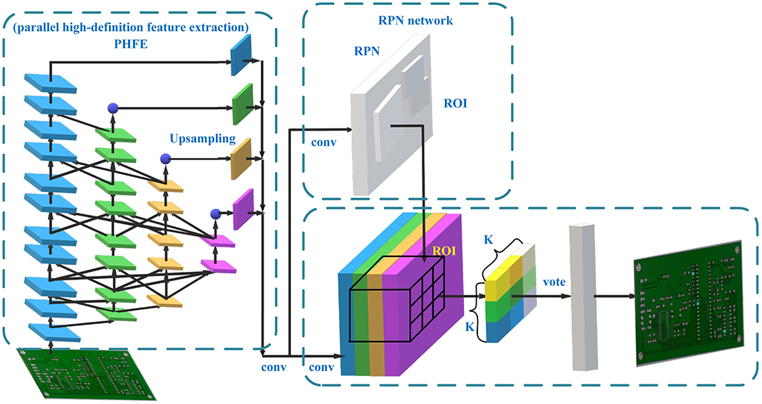
The structure of the minor defect recognition network in PCB proposed in this paper is shown in Figure 1. The network consists of four parts. The first part is the PCB image acquisition module, which uses industrial cameras to capture PCB images. The second part is the feature extraction part, which extracts convolutional features of different scales of PCB images. The third part is the minor defect area detection module, which conducts preliminary screening of areas that may be minor defects. The fourth part is to locate and identify minor defects.
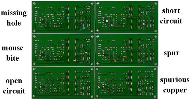
Industrial cameras can only photograph the surface of the PCB, so PCB defect detection based on machine vision is mainly aimed at minor defects on the surface of the PCB. These minor defects are mainly divided into six categories: missing hole, mouse bite, open circuit, short circuit, spur, and Spurious copper. Figure 2 shows six kinds of minor defects on the surface of the printed circuit board.
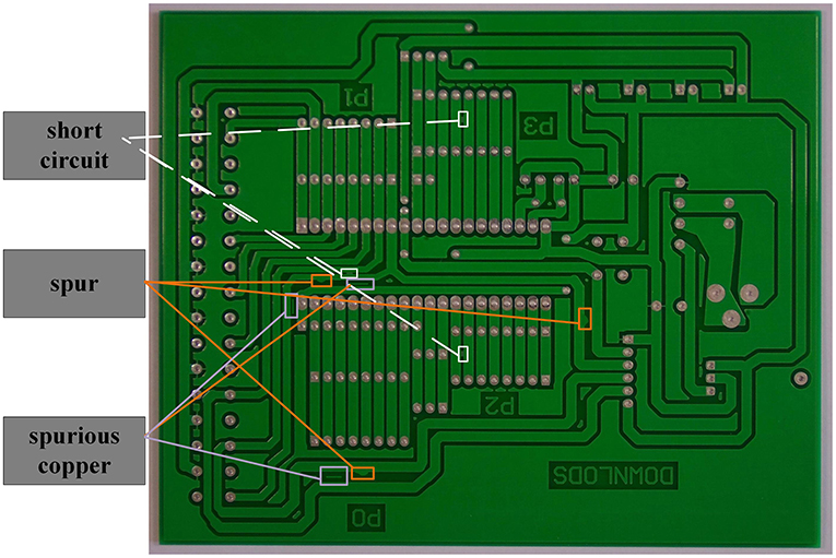
Minor defects account for a small proportion of the entire printed circuit board and the number is small, so there cause a problem of an imbalance between positive and negative samples. Firstly, in order to solve this problem, this paper uses data enhancement, which enhances the number of positive samples by randomly pasting defective areas to different positions. Figure 4 shows the PCB image after data enhancement. Secondly, because of the high complexity and similarity between different samples, a problem of difficulty in classification, which is also a special problem of sample imbalance, is generated. Therefore, in the fourth stage, this paper uses focal loss to optimize the RFCN target detection network, and proposes the FC-RFCN method to solve the problem of small target sample imbalance. Thirdly, in the deep convolutional neural network, the shallow network can retain more features of the original image, but the receptive field is smaller, and the deep feature receptive field is larger but will lose the features of the small target. The pixel values of the minor defects are all less. After multiple down-sampling, the deep features and the features of the small areas may be lost. The traditional target detection method is to simultaneously improve the detection rate of large and small targets through the fusion of convolutional layers of different scales. Since all minor defects of printed circuit boards are small targets, this paper proposes a PHFE method (parallel high-resolution feature extraction method) to improve the recognition rate of minor defects.
Image Acquisition and Data Enhancement of Minor Defects
The defects in the printed circuit board are small, so we need to choose a high-resolution camera for image acquisition. According to the classification of photosensitive chips, high-definition cameras are classified, which are mainly divided into two types: CCD camera and CMOS camera. The two cameras are mainly different in materials, and there is no essential difference in image acquisition. This article chooses the MER-231-41GM camera for PCB image acquisition, this camera has a large frame, less noise and global exposure function.
When choosing a camera lens, it should be noted that a larger lens can recognize a smaller target, but a smaller lens has a poorer ability to retain information on a large target. Therefore, this article chooses the m0814-mp2 lens as the data acquisition lens in the experiment. Both the aperture and focal length of the lens can be adjusted manually. The image resolution of the printed circuit board and the distance of the camera can be combined to calculate the true size of the tiny defect. Identifying the true size of the tiny defect can provide accurate data for the robot to automatically repair the PCB defect. Therefore, it is necessary to accurately measure the distance from the lens to the PCB surface. In this experiment, the distance between the camera and the printed circuit board is 160 mm.
Where, fCCD means focal length of high-resolution camera, dPCB represents the distance between the camera and the PCB, Hm represent the height of the imaging plane and Hn means the field of view of the lens focal length camera.
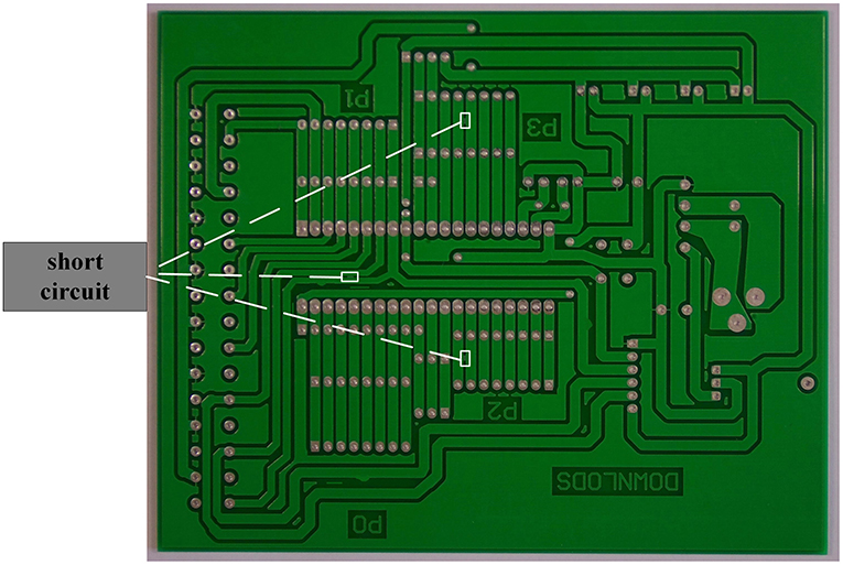
After building the PCB image collection platform, we collected PCB images with a resolution of 3,634 × 2,464. First, we use the tool named labelling to label minor defects in the PCB. The PCB image label with labelling is as shown in Figure 3. It can be seen that the number and area of minor defects in the printed circuit board are too small, and there only be one type of minor defect in a circuit board. Since most of the PCB images have very few minor defects, this paper randomly pastes the target area and replaces the background to enhance the positive samples. Figure 4 shows the printed circuit board image after data enhancement. It can be seen from Figure 4 that the types and number of minor defects in the printed circuit board image after data enhancement have increased.
Feature Extraction Method of Minor Defects of Printed Circuit Board Based on PHFE
The size of the original image collected by the camera is 3,634 × 2,464, and its size is too large. The image input to the neural network usually has a resolution of 640 × 640. So, we crop the image. Then, input the cropped PCB image into the neural network for minor defect recognition. Finally, the recognition results of the cropped images are stitched together. This also prevents the pixel values of tiny defects from being further lost during the image resize process.
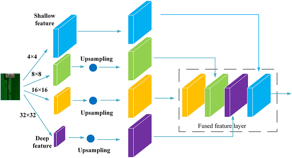
In order to improve the feature extraction ability of the network for small targets, the neural network is used to extract features from the PCB image. The characteristic pyramid is used to form a characteristic pyramid of four scales. The scales from low-rise to high-rise are 80 × 80, 40 × 40, 20 × 20, and 10 × 10. The area of the micro defect is small, and the feature of the micro defect will be lost in the feature layer after the size is 20 × 20. We propose a parallel high-definition feature extraction method, in which the bottom layer features are added every time the feature layers of different scales are fused, so that the features at the minor defects always exist in the feature map. Other defect feature extraction methods are simply superimposing feature layers of different sizes to fuse feature, and the feature extraction capabilities of network are not enhanced for small targets. The proposed method can increase the proportion of small target features in the feature map, which enhanced the feature extraction capabilities of network for minor defects.
Figure 5 shows the structure of the parallel high-definition feature extraction method. First, the PCB image uses 4 × 4, 8 × 8, and 16 × 16 convolution kernels for multi-scale feature extraction. [2] is the formula for feature extraction.
Where, Fj means the characteristic map of 4 × 4, 8 × 8, and 16 × 16 convolution output; X means the input data of the defect image in the printed circuit board; f means the activation function Relu; Wj is 4 × 4, 8 × 8, and 16 × 16 convolution kernel weights, respectively; Bj is the bias of 4 × 4, 8 × 8, and 16 × 16 convolution kernels, respectively.
The feature maps with sizes of 40 × 40 and 20 × 20 are, respectively, up-sampled at different scales and then merged with the 80 × 80 feature maps to form high-definition features of tiny defects. [3] is the calculation method for the fusion of feature layers of different scales.
Where, F1 is a feature map with a size of 10 × 10. F2 is a feature map with a size of 20 × 20. F3 is a feature map with a size of 40 × 40. F4 is a feature map with a size of 80 × 80, which is shallow feature map. F is the high-definition feature map, which is the result of feature map fusion by PHFE method.
Then, the feature maps with sizes of 40 × 40, 20 × 20, and 10 × 10 are up-sampled, and the size after up-sampling is consistent with the size of the shallow feature map. Finally, by adding together, the shallow features and the two up-sampled feature maps are fused to obtain a new feature layer, which is used as the input of the next layer of convolution to provide rich image feature information for the lower layer of convolution, thereby improving the feature extraction ability of the network model and the recognition rate of minor defects in the PCB. After multiple feature fusions, the high-definition feature map is obtained.
Recognition Method of Minor Defects of Printed Circuit Board Based on FL-RFCN
After the feature map is extracted, the feature map is sent to the RPN network to generate candidate frames that may exist in the minor defect area. Then classify the tiny areas in these candidate frames. Because minor defects occupy a small area in the printed circuit board, and there are problems of high complexity between different defects, this is a special data imbalance problem.
In the previous stage, the model simultaneously outputs four different scale feature maps of 80 × 80, 40 × 40, 20 × 20, and 10 × 10. Each pixel in the feature map is a cell, and each cell has three detection frames, that is, 2,550 detection frames are output at the same time. But only a very small part of the inspection frame contains the target, especially when the proportion of minor defects is small. Therefore, most of the detection frames will be marked as negative samples, and minor defects are positive samples. Therefore, during model training, the difference between the number of positive and negative samples is too large, so that negative samples dominate the direction of gradient update. The network cannot learn useful information, and the recognition rate of minor defects is reduced.
Therefore, this paper uses focal loss to optimize the loss function in RFCN, and proposes the FL-RFCN. By reducing the weight of negative samples in model training to correct the update direction of the model gradient, the network can learn more useful information and improve the recognition rate of minor defects.
In the RFCN network, the cross-entropy formula was originally used to calculate the confidence loss of negative samples. The formula is shown in [4].
Where, y means the real label, 1 means a positive sample, and 0 means a negative sample; y' means the predicted value, and its range is from 0 to 1.
For positive samples, the higher the detection rate, the smaller the value of the cross-entropy loss. For negative sample appearance, the lower the detection probability, the smaller the cross-entropy loss. Therefore, if a large number of negative classification samples are used for iterative training, the model cannot be optimized to an ideal state, resulting in a decrease in the detection rate of minor defects.
Focal loss is a new loss function to balance positive and negative samples, and its calculation formula is shown in [5].
Where, γ is the weighting factor, when γ = 0, formula of focal loss is same as the formula of cross entropy loss. When γ > 0, the loss function will reduce the calculation amount of easy-to-classify samples and increase the proportion of difficult-to-classify samples; α is a balance factor, used to adjust the imbalance of positive and negative samples. LFL is the loss function of focal loss.
Experiments and Analysis
Dataset
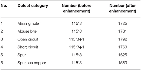
In this paper, 692 images of minor defects in printed circuit boards are collected. We divide the defect categories into six categories. Each category is selected about 115 images, and we use the labelme to label the data. The label content contains category information and location information of the minor defect. The number of defects in each printed circuit board picture is only 3. Therefore, we use data enhancement to expand the data volume. The data enhancement method used in this article is that randomly pastes the target area and replaces the background to enhance the positive samples. The categories and numbers of minor defects before and after data enhancement are shown in Table 1.
Tests and Results
mAP is the most commonly used and most important evaluation index in the target detection algorithm. It is one of the best evaluation criteria for the comprehensive performance of the model. Its calculation formula is shown in [6].
Where, APc is the average accuracy of each category, N(classes) is the number of categories in the minor defects.
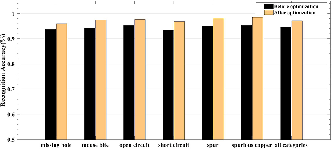
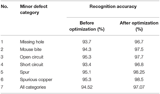
This article uses the parallel high-definition feature extraction method to improve the feature extraction capability of the neural network for small targets. Therefore, we designed a set of ablation experiments to compare the recognition accuracy of minor defects before and after the improvement under different data volumes. Figure 6 shows the accuracy comparison chart, and Table 2 shows the recognition accuracy of minor defects under different data volumes corresponding to Figure 6. It can be seen from the comparison that the parallel high-definition feature extraction method can effectively improve the detection rate of minor defects in the PCB.
In order to verify the adaptability of the FC-RFCN method. This article conducted related ablation experiments. Figure 7 shows the comparison results of mAP before and after optimization using focal loss under different data volumes. It can be seen from the figure that before optimization, as the sample size increases, the imbalance between positive and negative samples will expand. After using focal loss optimization, as the number of samples increases, the accuracy of minor defect recognition remains almost unchanged. Therefore, this verifies the effectiveness of FC-RFCN to solve the problem of sample imbalance.
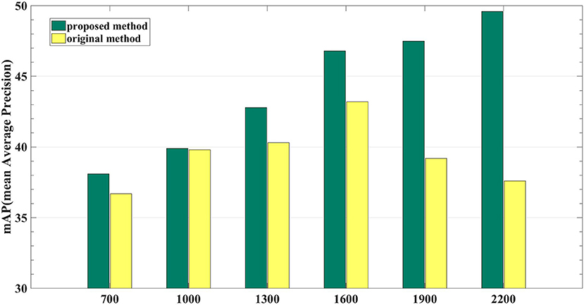
Figure 7. The comparison results of mAP before and after optimization using focal loss under different data volumes.
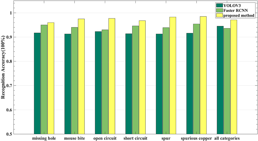
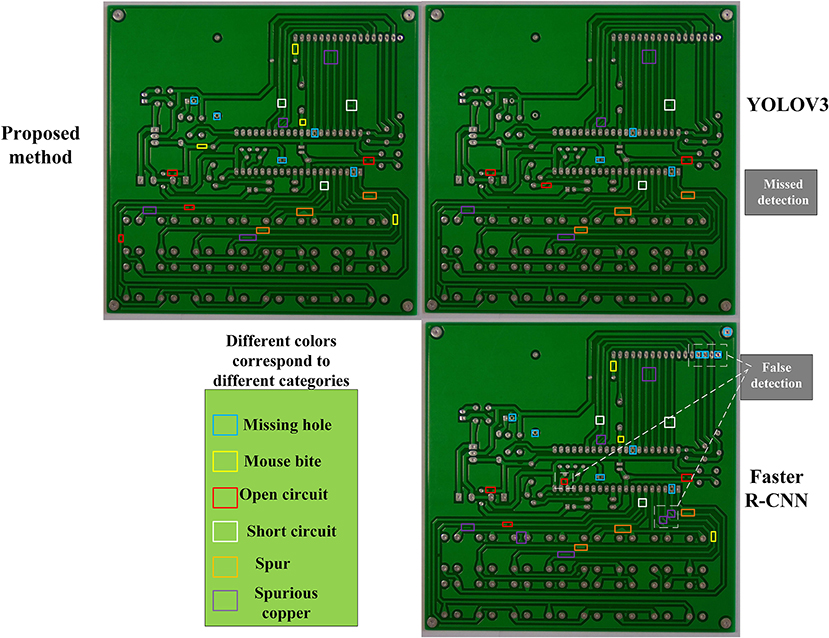
In order to more intuitively observe the advantages of the method in this paper compared with other target detection algorithms in PCB's minor defects. Compare the method proposed in this article with YOLO v3 and Faster RCNN. Figure 8 shows the average accuracy comparison results of different methods. In terms of recognition speed, Faster RCNN requires 0.15 s to recognize an image. YOLOv3 requires 0.031 s. The proposed method requires 0.089 s. It can be seen from Figure 8 that the recognition accuracy of the method in this paper is the highest, and the calculation speed of the method proposed is higher than Faster RCNN. Figure 9 is a comparison diagram of PCB identification effects of different methods. From Figure 9, it can be found that YOLOv3 has a large number of missed detections in the detection of small targets. Faster RCNN not only has the problem of missed detection of small targets, but also has a higher false detection rate. The method proposed in this paper can not only accurately identify all the minor defects, but also has a very low false detection rate. Therefore, the method in this paper is better than Faster RCNN and YOLOV3.
In terms of structure, compared with other deep learning methods, the proposed method can always retain the high-definition features of the first layer of the feature map in terms of structure. In terms of accuracy, the proposed method improves the detection rate of minor defects compared with traditional PCB inspection methods.
Conclusion
Aiming at the problem that it is difficult to identify the minor defects on the PCB surface, a minor defect detection method for printed circuit boards based on FL-RFCN and PHFE is designed. First use data enhancement to increase the amount of data in small areas. Then, use the PHFE method to extract the high-definition features of the small area, and finally use the Focal loss to optimize the RFCN network to solve the sample imbalance problem. Comparative experiments show that the accuracy of the network proposed in this paper is 97.3%, which is higher than other network models, and as the amount of data increases, the problem of sample imbalance will not affect the accuracy of the network. At the same time, the method in this paper can also be used to identify and locate circuit components in PCB boards. In future work, we will compress the network to improve its real-time performance.
Data Availability Statement
The original contributions presented in the study are included in the article/supplementary material, further inquiries can be directed to the corresponding author/s.
Author Contributions
SX and FW: conceptualization and writing—original draft preparation. FX and FW: methodology. SX and LH: software. FW, FX, and LH: validation. QW, FX, and XL: formal analysis. FW and XL: investigation. FX, XL, and LH: resources. QW and FX: data curation. FW, FX, and SX: writing—review and editing. FW: visualization. FX and SX: supervision. All authors have read and agreed to the published version of the manuscript.
Funding
This work was partially supported by the National Key Research and Development Program of China (Grant No. 2017YFB1103200), the National Natural Science Foundation of China (Grant Nos. 41974033 and 61803208), the Scientific and Technological Achievements Program of Jiangsu Province (BA2020004), and 2020 Industrial Transformation and Upgrading Project of Industry and Information Technology Department of Jiangsu Province. Postgraduate Research & Practice Innovation Program of Jiangsu Province (KYCX20_1257).
Conflict of Interest
The authors declare that the research was conducted in the absence of any commercial or financial relationships that could be construed as a potential conflict of interest.
Acknowledgments
The authors gratefully acknowledges the helpful comments and suggestions of the reviewers.
References
1. Zhang C, Shi W, Li X, Zhang H, Liu H. Improved bare PCB defect detection approach based on deep feature learning. J Eng. (2018) 16:1415–20. doi: 10.1049/joe.2018.8275
2. Li Y, Kuo P, Guo J. Automatic industry PCB Board DIP process defect detection system based on deep ensemble self-adaption method. IEEE Trans Comp Packag Manuf Technol. (2021) 11:312–23. doi: 10.1109/TCPMT.2020.3047089
3. Wei P, Liu C, Liu M, Gao Y, Liu H. CNN-based reference comparison method for classifying bare PCB defects. J Eng. (2018) 16:1528–33. doi: 10.1049/joe.2018.8271
4. Gaidhane V, Hote Y, Singh V. An efficient similarity measure approach for PCB surface defect detection. Patter Anal Appl. (2018) 21:277–89. doi: 10.1007/s10044-017-0640-9
5. Lin T, Goyal P, Girshick R, He K, Dollar P. Focal loss for dense object detection. IEEE Trans Pattern Anal Mach Intell. (2020) 42:318–27. doi: 10.1109/TPAMI.2018.2858826
6. Shi W, Lu Z, Wu W, Liu H. Single-shot detector with enriched semantics for PCB tiny defect detection. J Eng. (2020) 13:366–72. doi: 10.1049/joe.2019.1180
7. Tang C, Chen S, Zhou X, Ruan S, Wen H. Small-scale face detection based on improved R-FCN. Appl Sci. (2020) 10:1–16. doi: 10.3390/app10124177
8. Song J, Kim Y, Park TH. Defect classification method of PCB solder joint by color features and region segmentation. J Inst Control Robot Syst. (2017) 23:1086–91. doi: 10.5302/J.ICROS.2017.17.0187
9. Wu D, Wu Q, Yin X, Jiang B, Wang H, He D, et al. Lameness detection of dairy cows based on the YOLOv3 deep learning algorithm and a relative step size characteristic vector. Biosyst Eng. (2020) 189:150–63. doi: 10.1016/j.biosystemseng.2019.11.017
Keywords: printed circuit board, minor defect, data enhancement, focal loss, high-definition feature extraction
Citation: Xia S, Wang F, Xie F, Huang L, Wang Q and Ling X (2021) An Efficient and Robust Target Detection Algorithm for Identifying Minor Defects of Printed Circuit Board Based on PHFE and FL-RFCN. Front. Phys. 9:661091. doi: 10.3389/fphy.2021.661091
Received: 30 January 2021; Accepted: 14 April 2021;
Published: 10 May 2021.
Edited by:
Lei Guo, The University of Queensland, AustraliaCopyright © 2021 Xia, Wang, Xie, Huang, Wang and Ling. This is an open-access article distributed under the terms of the Creative Commons Attribution License (CC BY). The use, distribution or reproduction in other forums is permitted, provided the original author(s) and the copyright owner(s) are credited and that the original publication in this journal is cited, in accordance with accepted academic practice. No use, distribution or reproduction is permitted which does not comply with these terms.
*Correspondence: Fei Xie, eGllZmVpQG5qbnUuZWR1LmNu
 Siyu Xia1
 Fan Wang
 Fei Xie
 Lei Huang