
94% of researchers rate our articles as excellent or good
Learn more about the work of our research integrity team to safeguard the quality of each article we publish.
Find out more
ORIGINAL RESEARCH article
Front. Phys., 26 March 2021
Sec. Optics and Photonics
Volume 9 - 2021 | https://doi.org/10.3389/fphy.2021.659782
This article is part of the Research TopicPhysical Model and Applications of High-Efficiency Electro-Optical Conversion DevicesView all 24 articles
 Jingda Zhao1,2
 Xin Wang2*Yuzhu Pan2Yubing Xu2Yuwei Li2Jing Chen2Jun Wu2Qing Li2Zhiwei Zhao2Xiaobing Zhang2Javed Akram3Byung Seong Bae4Haining Yang2Wei Lei2*
Organic-inorganic hybrid methylammonium lead halide perovskite MAPbX3 (where MA = CH3NH3, and X = Cl, Br, I) single crystals are potential semiconductors for photo-detection due to their excellent optoelectronic performance. In particular, MAPbCl3 single crystal is a wide-band-gap (2.9 eV) semiconductor which is suitable for ultraviolet (UV) detection. In this work, n−-n+ photo-diodes are fabricated through solution-processed epitaxial growth, growing Bi-doped MAPbCl3 epitaxial layer on MAPbCl3 single crystal substrate. The epitaxial layer effectively improves the interface between n−-type and n+-type layers and leads to low dark current. This work provides useful information for UV detection based on perovskites.
Recently, Organic-inorganic hybrid methylammonium lead halide perovskite (MAPbX3, where MA = CH3NH3, and X = Cl, Br, I) perovskite have attracted a lot of attention due to their excellent optoelectronic properties, such as tunable band gap, low trap density, and long diffusion length [1, 2]. MAPbX3 have been proved to have potential in a number of optoelectronic devices, such as photodetectors, light-emitting diodes, and solar cells [3–9]. There are reports on the visible and near infrared detection applications of MAPbI3 and MAPbBr3 single crystals because of their suitable band gap and high optical absorption coefficient [10, 11]. MAPbCl3 single crystals are wide-bandgap (2.9 eV) semiconductors [12] which are insensitive to visible light while having a high absorption for ultraviolet (UV) radiation (wavelength ~100–400 nm) [13]. These characters make MAPbCl3 single crystals suitable in applications of UV detection [14–16]. To best our knowledge, little work carried out to study the optoelectronic characteristics of photo-diode based on MAPbCl3, which is important to develop optoelectronic device based on PSCs. Therefore, it is necessary to obtain a photo-diode based on MAPbCl3 with high performance.
The properties of conventional semiconductor could be adjusted by impurity doping, similarly, heterovalent metals doping into PSCs is an efficient way to change the electrical and optical properties [17–21]. MAPbCl3 is proved to be a n− type semiconductor [12], while doping Bi3+ into MAPbX3 would move Femi level close to conduction band [22, 23]. Inspired by the above work, we suppose to fabricate n−-n+ photo-diodes based on n−-type MAPbCl3 single crystal substrate with n+-type Bi-doped MAPbCl3 epitaxial layer. Different to conventional heterojunction, the PSCs homojunction has low lattice mismatch rate, continuous band alignments, and low trap densities [24–26] which allow the device to have a lower dark current when the device is under reverse bias.
In this work, a bulk MAPbCl3 single crystal with cubic shape and high crystallization quality was synthesized by inverse temperature crystallization (ITC) method [27], and we fabricated a UV photo-diode by growing Bi-doped MAPbCl3 epitaxial layer on MAPbCl3 single crystal substrate. This photo-diode shows a low dark current density of −2.15 μAcm−2 at −20 V bias voltage while its photocurrent reaches −82.69 μAcm−2 under 393 nm LED with the illumination of 20 mWcm−2. Due to the successful fabricating of the n−-n+ junction, the responsibility reaches 404.7 mA/W, ~1–2 orders of magnitude higher than pervious reported photodetector based on MAPbCl3 [14, 28], and its detectivity reaches 4.87 × 10¹¹ Jones, which is two orders of magnitude higher than that of the previously reported MAPbCl3 photodetectors [14]. The relatively high carrier mobility makes the rise time reach 176.3 ns while decay reaches 11.6 μs, which is 1–3 orders of magnitude faster than that of the previously reported MAPbCl3 photodetectors [14, 15, 28].
Lead chloride (PbCl2, 99%) were purchased from Sigma Aldrich. N, N-Dimethylformamidel (DMF, 99.5%), and Dimethyl sulfoxide were purchased from Chinese reagents. Bismuth Chloride (BiCl3, 98%) and Methylamine hydrochloride (MACl, 98%) were purchased from Aladdin. All commercial products were used as received.
1 mol/L MACl and 1 mol/L PbCl2 were dissolved in 50 ml dimethylformamide (DMF) and dimethylsulfoxide (DMSO) mixed solution (1:1 v/v) to act as precursor solutions. The poly tetra fluoroethylene (PTFE) filters with a 30 μm pore size were used to filter the solutions. Then, the precursor solutions, after being filtered, were transferred to a crystallizing dish by dropper. The crystallizing dish was placed on a programmable heating station (IKA-RET control-visc). The temperature was set to rise 0.5°C per hour from 40 to 60°C, the whole process is shown in Figure 1A. After two days, the pristine MAPbCl3 single crystal could be obtained, Figure 1B shows the MAPbCl3 substrate with the size of 6.95 × 6.96 × 2.52 mm.
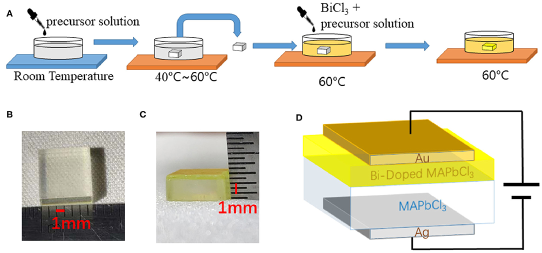
Figure 1. (A) Processing of the growth of PSC and epitaxial. (B) Optical photo of pristine MAPbCl3 PSC. (C) Optical photo of MAPbCl3 single crystal with Bi-doped MAPbCl3 epitaxial layer. (D) Schematic representation of the photodiode structure.
Similarly, 1 mol/L MACl, 1 mol/L PbCl2, and 0.1 mol/l BiCl3 were dissolved in 10 ml dimethylformamide (DMF) and dimethylsulfoxide (DMSO) mixed solution (1:1 v/v) to prepare for epitaxial growth. The pristine MAPbCl3 single crystal was put into the epitaxial solution. After the heating station temperature kept at 60°C for 4 h. the MAPbCl3 with epitaxial layer could be obtained, and Figure 1C is a photograph of MAPbCl3 single crystal with epitaxial layer after polishing the edges of the crystal, obviously, the color of the epitaxial layer is yellow and the thickness of the epitaxial layer is nearly 0.52 mm. To fabricated the photo-diodes, the gold electrode acted as anode is deposited on the side of the MAPbCl3 substrate while the sliver electrode acted as cathode is deposited on the side of the epitaxial layer. The structure of this device is shown in Figure 1D.
X-ray diffraction (XRD) patterns were taken by X'TRA (Switzerland). Photoluminescence (PL) spectra were measured by UV–vis spectroscopy (Lab Tech Bluestar, USA). I-V curve was measured by a Keithley 4200 semiconductor analyzer. EQE was measured by Zolix tunable 500-W arc lamplight. A 355-nm pulsed Nd: YAG laser with 6-ns pulse width at 10 Hz as the illumination source and an Agilent oscilloscope were used to measure the carrier mobility.
Firstly, we study the optical properties of the pristine MAPbCl3 substrate, MAPbCl3 with Bi-doped MAPbCl3 epitaxial layer, and Bi-doped MAPbCl3 single crystal, the PL spectra and absorption are shown in Figures 2A,B. The absorption edge of pristine MAPbCl3 single crystal was located at 430 nm, and the PL peak is obtained at 436 nm with a narrow FWHM of 14.9 nm confirming the high quality of the single crystal [7]. Doping into single crystal would cause a larger increase of the lattice defect which is the reason why the PL of the Bi-doped MAPbCl3 has a broadening effect [29]. The absorption of Bi-doped MAPbCl3 single crystal is in good agreement with results that were previously reported [30]. The PL of MAPbCl3 with Bi-doped MAPbCl3 epitaxial layer is the stack of the pristine MAPbCl3 and Bi-doped MAPbCl3 single crystal, which indicated the successful growth of the Bi-doped MAPbCl3 epitaxial layer. The absorption moves from 430 to 480 nm after epitaxial growth which approaches the Bi-doped MAPbCl3 single crystal.
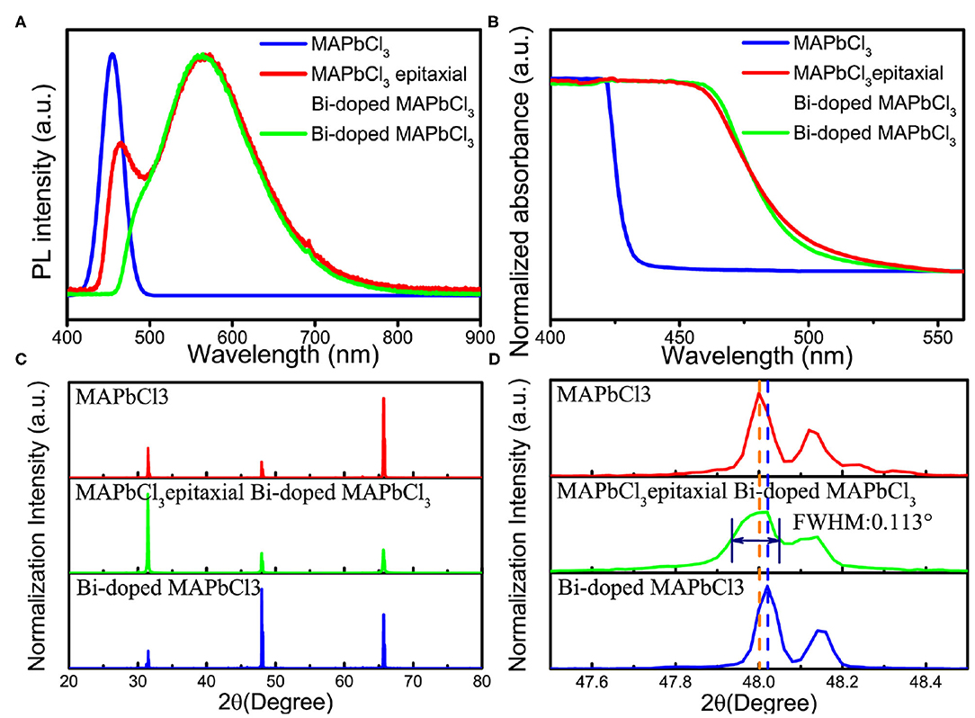
Figure 2. (A) PL spectra of pristine MAPbCl3 substrate, MAPbCl3 with epitaxial layer, and Bi-doped MAPbCl3. (B) Absorption of pristine MAPbCl3 substrate, MAPbCl3 with epitaxial layer, and Bi-doped MAPbCl3. (C) XRD spectra of the pristine MAPbCl3 substrate, MAPbCl3 with Bi-doped MAPbCl3 epitaxial layer, and Bi-doped MAPbCl3 single crystal. (D) XRD spectra from 47.5° to 48.5° of the three kinds of PSCs.
Figures 2C,D provide XRD spectra of pristine MAPbCl3 single crystal, MAPbCl3 with epitaxial layer, and Bi-doped MAPbCl3. To (100) planes, the strongest peaks of MAPbCl3 are observed at 2θ = 31.48°, 48.00°, 65.68°, while the strongest peaks of Bi-doped MAPbCl3 at 2θ = 31.50°, 48.02°, 65.70° indicating no phase change after doping Bi3+. Besides, Figure 2D illustrates the FWHM of pristine MAPbCl3 single crystal with the epitaxial layer is 0.113° which confirms the epitaxial layer remains single crystalline. The stagger XRD peak of MAPbCl3 substrate and epitaxial layer causes the FWHM of photo-diode to be widened. The lattice constants could be calculated from the XRD spectra by Bragg law (2dsinθ = n*λ, where d is the distance between two atoms, θ is the angle of crystal plane and X-ray, n is constant, and λ is the wavelength of the X-ray), the lattice constants of MAPbCl3 and Bi-doped MAPbCl3 are 5.67902 Å and 5.67550 Å, respectively, the lattice constants of MAPbCl3 is same as previously reported [31]. After doping Bi3+, the lattice constant is smaller than pristine MAPbCl3 single crystal indicating the Bi3+ ions are possibly substituting Pb2+ ions in the crystal. The mismatch rate (mismatch rate can be calculated by γ = (a1−a2)/(a1 + a2), where ai is the lattice constants of the crystal) of MAPbCl3 and Bi-doped MAPbCl3 single crystal is 0.3%, suggesting that their lattice could match well.
Further, the charge mobility of the photo-diode is investigated by the TOF method. After the optical signal is received, the photo-induced holes could immediately be collected under forward bias, while electrons have to drift through the whole device to be collected, the electrons mobility could be calculated through the drift time. Similarly, under the reverse voltage, the holes' mobility could be calculated in the same way. A 355-nm pulsed Nd: YAG laser with 6-ns pulse width at 10 Hz is used as the illumination source, the direction of the light is shown in Figure 3A. The average electron mobility was measured as shown in Figure 3B. And the average hole mobility was measured as shown in Figure 3C. The carrier mobility can be calculated according to:
where μ is the carrier mobility, L is the thickness of the photo-diode, Vs is the bias voltage between two electrodes, and Ttof is the transmit time [32, 33]. The fitting plot of carrier mobility vs. reciprocal of the bias voltage is shown in the insets, the result shows that the average holes mobility is 55.06 ± 0.61 cm2V−1s−1 is faster than UV detector based on MAPbCl3 single crystal (26 cm2V−1s−1) reported [16], the reason is Bi-Doped MaPbCl3 has a high conductivity. And the average electrons mobility is 40.01 ± 1.30 cm2V−1s−1.
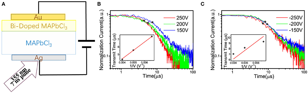
Figure 3. (A) Illustration of the optoelectronic experiment. (B) Holes mobility measured by time-of-flight (TOF) method. (C) Electrons mobility measured by the TOF method.
Figure 4A illustrates the EQE of the photo-diode under −20V, the EQE peak locates at 398 nm which prove the device can be applied in UV photo-detection. EQE is calculated by:
where ILight is the photocurrent (A), IDark is the dark current (A), h is Plank's constant, ν is the frequency of incident light, S is the area being illuminated, and P is the incident illumination power density (W/cm2), and e is the element charge [34].
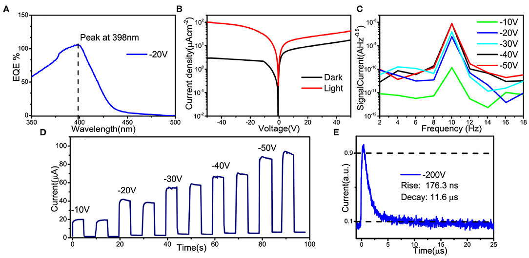
Figure 4. (A) EQE curve under −20 V from 350 to 500 nm. (B) Current density vs. Voltage curve. (C) Signal current as a function of frequency under different voltage bias. (D) Temporal response of the photo-diode under different Voltage. (E) Rise time and decay time of the photo-diode at −200 V bias.
To further study the optoelectronic performance of this photo-diode, an LED with an emission peak of 393 nm and the power intensity of the LED is 20 mWcm−2, and the current-voltage characterization of the device in the dark and under illumination is shown in Figure 4B, respectively. The photocurrent under reverse bias is much larger than the photocurrent under forward bias. Because of the built-in electric field, holes are hard to transfer from MAPbCl3 substrate to Bi-MAPbCl3 epitaxial layer and electrons are hard to transfer from Bi-MAPbCl3 epitaxial layer to MAPbCl3 substrate when the device is under reverse bias and in a dark environment, and the homojunction restrains the dark current further. Thanks to the highly crystallized epitaxial layer, the dark current of the photo-diode is −2.15 μAcm−2 at −20 V, while its photocurrent reaches approximately −82.69 μAcm−2 under illumination. To analyze the response ability of the photo-diode to UV radiation, the responsivity (R) and detectivity (D) of the photo-diode was calculated as follow [35, 36]:
The responsivity is calculated to be 404.7 mA/W, detectivity is calculated to be 4.87 × 10¹¹ Jones which is one order of magnitude larger compared to MAPBCl3 film (6.87 × 10¹⁰ Jones) [37].
To study the signal noise at low frequency, we investigate 10 Hz temporal response of the photo-diode under different reverse voltage bias from −10 to −50 V, the Fast Fourier Transform (FFT) method is used to transfer the current vs. time curve to signal current vs. frequency curve. The signal noise from 2 to 18 Hz is calculated and the curve is shown in Figure 4C. The average noise current increases from 2.3 pAHz−0.5 to 17.0 nAHz−0.5 under illumination with bias voltage from −10 to −50 V.
Figure 4D illustrates the on–off switching properties of the photo-diode with the bias voltage range from −10 to −50 V. Obviously, the photo-diode could switch rapidly and stably under different bias. The response speed was measured as shown in Figure 4E, the rise time is 176.3 ns and the fall time is 11.6 μs under the bias of −150 V, the fast carrier mobility contributes to the rapid response speed.
The comparison of responsivity and response time between this work and previously reported MAPbCl3 photodetector is summarized in Table 1. The photo-diode fabricated in this work has a higher responsivity than most UV detectors reported, and the decay time is the fastest.
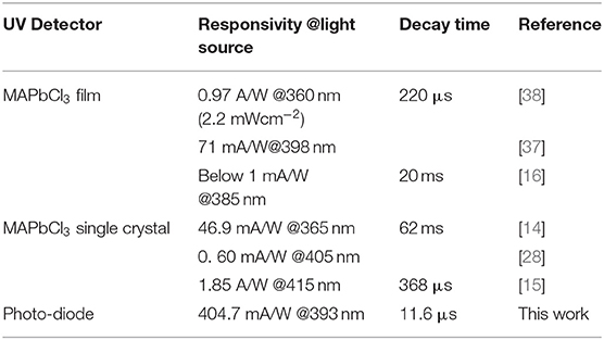
Table 1. Comparison between this work and previously reported MAPbCl3 photodetectors.
In summary, we have fabricated a UV photo-diode by growing Bi-doped MAPbCl3 epitaxial layer on a pristine MAPbCl3 single crystal substrate. And we calculate the lattice constants of pristine MAPbCl3 and Bi-doped MAPbCl3 single crystal through XRD, which are lattice-matched. Further, we investigate the optoelectronic properties of the photo-diode. At −20 V voltage, the dark current is −2.15 μAcm−2 while the photocurrent reaches −82.69 μAcm−2, the on-off ratio reaches nearly 40 under a 393 nm LED with 20 mW/cm2. Moreover, the photo-diode has a responsivity of 404.7 mW/cm2 and detectivity of 4.87 × 10¹¹ Jones. The carrier mobility is calculated to be 55.06 ± 0.61 cm2V−1s−1 by TOF. The rise time and decay time are 176.3 ns and 11.6 μs, which is faster than the previously reported UV detector based on MAPbCl3 single crystal and ploy-crystal film. This work provides useful information for UV detection and photoelectrical device based on MAPbX3.
The raw data supporting the conclusions of this article will be made available by the authors, without undue reservation.
JZ and YP grew the perovskite single crystals. JZ did the epitaxial experiments. YX and JZ did the measurements. XW and JZ analyzed these results. JZ wrote this manuscript. All authors make comments on the manuscript.
This work was financially supported by the funding of State Key Laboratory of Nuclear Power Safety Monitoring Technology and Equipment (K-A2020.415), National Key Research and Development Program of China (2018YFE0125500, 2016YFB0401600), Program 111_2.0 in China (BP0719013), National Natural Science Foundation Project of China (61775034, 51879042, 61674029, 12005038), Research Fund for International Young Scientists (62050410350), International Cooperative Research Project of Jiangsu Province (BZ2018056), Leading Technology of Jiangsu Basic Research Plan (BK20192003).
JZ is employed by China Nuclear Power Engineering Co. Ltd., Shenzhen, Guangzhou, China.
The remaining authors declare that the research was conducted in the absence of any commercial or financial relationships that could be construed as a potential conflict of interest.
1. Shi D, Adinolfi V, Comin R, Yuan M, Alarousu E, Buin A, et al. Low trap-state density and long carrier diffusion in organolead trihalide perovskite single crystals. Science. (2015) 347:519–22. doi: 10.1126/science.aaa2725
2. Dong. Electron-hole diffusion lengths >175 μm in solution-grown CH3NH3PbI3 single crystals. Sci Expr. (2015) 43210:1–8. doi: 10.1126/science.aaa5760
3. Yusoff ARBM, Nazeeruddin MK. Organohalide lead perovskites for photovoltaic applications. J Phys Chem Lett. (2016) 7:851–66. doi: 10.1021/acs.jpclett.5b02893
4. Jena AK, Kulkarni A, Miyasaka T. Halide perovskite photovoltaics: background, status, and future prospects. Chem Rev. (2019) 119:3036–103. doi: 10.1021/acs.chemrev.8b00539
5. Jaramillo-Quintero OA, Sanchez RS, Rincon M, Mora-Sero I. Bright visible-infrared light emitting diodes based on hybrid halide perovskite with Spiro-OMeTAD as a hole-injecting layer. J Phys Chem Lett. (2015) 6:1883–90. doi: 10.1021/acs.jpclett.5b00732
6. Wehrenfennig C, Liu M, Snaith HJ, Johnston MB, Herz LM. Homogeneous emission line broadening in the organo lead halide perovskite CH3NH3PbI3−xClx. J Phys Chem Lett. (2014) 5:1300–6. doi: 10.1021/jz500434p
7. Veldhuis SA, Boix PP, Yantara N, Li M, Sum TC, Mathews N, Mhaisalkar SG. Perovskite materials for light-emitting diodes and lasers. Adv Mater. (2016) 28:6804–34. doi: 10.1002/adma.201600669
8. Pan Y, Wang X, Xu Y, Li Y, Elemike EE, Shuja A, et al. Enhanced performance of perovskite single-crystal photodiodes by epitaxial hole blocking layer. Front Chem. (2020) 8:791. doi: 10.3389/fchem.2020.00791
9. Xu Y, Wang X, Pan Y, Li Y, Emeka Elemike E, Li Q, et al. Perovskite photodetectors based on p-i-n junction with epitaxial electron-blocking layers. Front Chem. (2020) 8:811. doi: 10.3389/fchem.2020.00811
10. Yakunin S, Dirin DN, Shynkarenko Y, Morad V, Cherniukh I, Nazarenko O, et al. Detection of gamma photons using solution-grown single crystals of hybrid lead halide perovskites. Nat Photon. (2016) 10:585–9. doi: 10.1038/nphoton.2016.139
11. Xu Q, Shao W, Li Y, Zhang X, Ouyang X, Liu J, et al. High-performance surface barrier x-ray detector based on methylammonium lead tribromide single crystals. ACS Appl Mater Interfaces. (2019) 11:9679–84. doi: 10.1021/acsami.8b21605
12. Liu Y, Yang Z, Cui D, Ren X, Sun J, Liu X, et al. Two-inch-sized perovskite CH3NH3PbX3 (X = Cl, Br, I) crystals: growth and characterization. Adv Mater. (2015) 27:5176–83. doi: 10.1002/adma.201502597
13. Li D, Jiang K, Sun X, Guo C. AlGaN photonics: recent advances in materials and ultraviolet devices. Adv Opt Photon. (2018) 10:43. doi: 10.1364/AOP.10.000043
14. Maculan G, Sheikh AD, Abdelhady AL, Saidaminov MI, Haque MA, Murali B, et al. CH3NH3PbCl3 single crystals: inverse temperature crystallization and visible-blind UV-photodetector. J Phys Chem Lett. (2015) 6:3781–6. doi: 10.1021/acs.jpclett.5b01666
15. Cheng Z, Liu K, Yang J, Chen X, Xie X, Li B, et al. High-performance planar-type ultraviolet photodetector based on high-quality CH3NH3PbCl3 perovskite single crystals. ACS Appl Mater Interfaces. (2019) 11:34144–50. doi: 10.1021/acsami.9b09035
16. Adinolfi V, Ouellette O, Saidaminov MI, Walters G, Abdelhady AL, Bakr OM, et al. Fast and sensitive solution-processed visible-blind perovskite UV photodetectors. Adv Mater. (2016) 28:7264–8. doi: 10.1002/adma.201601196
17. Klug MT, Osherov A, Haghighirad AA, Stranks SD, Brown PR, Bai S, et al. Tailoring metal halide perovskites through metal substitution: Influence on photovoltaic and material properties. Energy Environ Sci. (2017) 10:236–46. doi: 10.1039/C6EE03201J
18. Sarkar P, Srivastava A, Tripathy SK, Baishnab KL, Lenka TR, Menon PS, et al. Exploring the effect of Ga3+ doping on structural, electronic and optical properties of CH3NH3PbCl3 perovskites: an experimental study. J Mater Sci Mater Electron. (2020). doi: 10.1007/s10854-020-04019-w. [Epub ahead of print].
19. Zhang J, Shang MH, Wang P, Huang X, Xu J, Hu Z, et al. N-type doping and energy states tuning in CH3NH3Pb1−xSb2x/3I3 perovskite solar cells. ACS Energy Lett. (2016) 1:535–41. doi: 10.1021/acsenergylett.6b00241
20. Choi H, Jeong J, Kim HB, Kim S, Walker B, Kim GH, et al. Cesium-doped methylammonium lead iodide perovskite light absorber for hybrid solar cells. Nano Energy. (2014) 7:80–85. doi: 10.1016/j.nanoen.2014.04.017
21. Xiong Y, Xu L, Wu P, Sun L, Xie G, Hu B. Bismuth doping–induced stable seebeck effect based on MAPbI3 polycrystalline thin films. Adv Funct Mater. (2019) 29:1–10. doi: 10.1002/adfm.201900615
22. Li C, Chen X, Li N, Liu J, Yuan B, Li Y, et al. Highly conductive n-type CH3NH3PbI3 single crystals doped with bismuth donors. J Mater Chem C. (2020) 8:3694–704. doi: 10.1039/C9TC06854F
23. Abdelhady AL, Saidaminov MI, Murali B, Adinolfi V, Voznyy O, Katsiev K, et al. Heterovalent dopant incorporation for bandgap and type engineering of perovskite crystals. J Phys Chem Lett. (2016) 7:295–301. doi: 10.1021/acs.jpclett.5b02681
24. Shah JM, Li YL, Gessmann T, Schubert EF. Experimental analysis and theoretical model for anomalously high ideality factors (n≫2.0) in AlGaN/GaN p-n junction diodes. J Appl Phys. (2003) 94:2627–30. doi: 10.1063/1.1593218
25. Jin Y, Keum DH, An SJ, Kim J, Lee HS, Lee YH. A Van der waals homojunction: ideal p-n diode behavior in MoSe2. Adv Mater. (2015) 27:5534–40. doi: 10.1002/adma.201502278
26. Li F, Li J, Gao L, Long X, Hu Y, Wang C, et al. Facile regrowth of Mg-Fe2O3/P-Fe2O3 homojunction photoelectrode for efficient solar water oxidation. J Mater Chem A. (2018) 6:13412–8. doi: 10.1039/C8TA05194A
27. Saidaminov MI, Abdelhady AL, Murali B, Alarousu E, Burlakov VM, Peng W, et al. High-quality bulk hybrid perovskite single crystals within minutes by inverse temperature crystallization. Nat Commun. (2015) 6:8586. doi: 10.1038/ncomms8586
28. Cheng X, Jing L, Zhao Y, Du S, Ding J, Zhou T. Crystal orientation-dependent optoelectronic properties of MAPbCl3 single crystals. J Mater Chem C. (2018) 6:1579–86. doi: 10.1039/C7TC05156E
29. Wang R, Zhang X, He J, Ma C, Xu L, Sheng P, Huang F. Bi3+-doped CH 3 NH 3 PbI 3: red-shifting absorption edge and longer charge carrier lifetime. J Phys Chem C. (2017) 695:555–60. doi: 10.1016/j.jallcom.2016.11.125
30. Zhang Z, Ren L, Yan H, Guo S, Wang S, Wang M, et al. Bandgap narrowing in bi-doped CH3NH3PbCl3 perovskite single crystals and thin films. J Phys Chem C. (2017) 121:17436–41. doi: 10.1021/acs.jpcc.7b06248
31. Baikie T, Barrow NS, Fang Y, Keenan PJ, Slater PR, Piltz RO, et al. A combined single crystal neutron/X-ray diffraction and solid-state nuclear magnetic resonance study of the hybrid perovskites CH3NH3PbX3(X=I,Br and Cl). J Phys Chem C. (2015) 3:9298–307. doi: 10.1039/C5TA01125F
32. Huang J, Shao Y, Dong Q. Organometal trihalide perovskite single crystals: a next wave of materials for 25% efficiency photovoltaics and applications beyond J Phys Chem Lett. (2015) 6:3218–27. doi: 10.1021/acs.jpclett.5b01419
33. Thirimanne HM, Jayawardena KDGI, Parnell AJ, Bandara RMI, Karalasingam A, Pani S, et al. High sensitivity organic inorganic hybrid X-ray detectors with direct transduction and broadband response. Nat Commun. (2018) 9:2926. doi: 10.1038/s41467-018-05301-6
34. Li C, Wang H, Wang F, Li T, Xu M, Wang H, et al. Ultrafast and broadband photodetectors based on a perovskite/organic bulk heterojunction for large-dynamic-range imaging. Light Sci Appl. (2020) 9:31. doi: 10.1038/s41377-020-0264-5
35. Dou L, Yang YM, You J, Hong Z, Chang WH, Li G, Yang Y. Solution-processed hybrid perovskite photodetectors with high detectivity. Nat Commun. (2014) 5:5404. doi: 10.1038/ncomms6404
36. Li C, Lu J, Zhao Y, Sun L, Wang G, Ma Y. Highly sensitive, fast response perovskite photodetectors demonstrated in weak light detection circuit and visible light communication system. Small. (2019) 15:e1903599. doi: 10.1002/smll.201903599
37. Zheng E, Yuh B, Tosado GA, Yu Q. Solution-processed visible-blind UV-A photodetectors based on CH3NH3PbCl3 perovskite thin films. J Mater Chem. (2017) 5:3796–806. doi: 10.1039/C7TC00639J
Keywords: UV detection, perovskite, single crystal, epitaxial growth, photo-diodes
Citation: Zhao J, Wang X, Pan Y, Xu Y, Li Y, Chen J, Wu J, Li Q, Zhao Z, Zhang X, Akram J, Bae BS, Yang H and Lei W (2021) Photo-Diodes Based on CH3NH3PbCl3 Perovskite Single Crystals by Epitaxial Growth for Ultraviolet Photo-Detection. Front. Phys. 9:659782. doi: 10.3389/fphy.2021.659782
Received: 28 January 2021; Accepted: 25 February 2021;
Published: 26 March 2021.
Edited by:
Feng Chi, University of Electronic Science and Technology of China, ChinaReviewed by:
Liming Liu, University of Electronic Science and Technology of China, ChinaCopyright © 2021 Zhao, Wang, Pan, Xu, Li, Chen, Wu, Li, Zhao, Zhang, Akram, Bae, Yang and Lei. This is an open-access article distributed under the terms of the Creative Commons Attribution License (CC BY). The use, distribution or reproduction in other forums is permitted, provided the original author(s) and the copyright owner(s) are credited and that the original publication in this journal is cited, in accordance with accepted academic practice. No use, distribution or reproduction is permitted which does not comply with these terms.
*Correspondence: Xin Wang, MjMwMTU5NDI0QHNldS5lZHUuY24=; Wei Lei, bHdAc2V1LmVkdS5jbg==
Disclaimer: All claims expressed in this article are solely those of the authors and do not necessarily represent those of their affiliated organizations, or those of the publisher, the editors and the reviewers. Any product that may be evaluated in this article or claim that may be made by its manufacturer is not guaranteed or endorsed by the publisher.
Research integrity at Frontiers
Learn more about the work of our research integrity team to safeguard the quality of each article we publish.