 Mara Bruzzi1,2*
 Cinzia Talamonti2,3
- 1Dipartimento di Fisica e Astronomia, Università degli Studi di Firenze, Firenze, Italy
- 2Istituto Nazionale di Fisica Nucleare, Sezione di Firenze, Firenze, Italy
- 3Dipartimento di Scienze Biomediche Sperimentali e Cliniche “Mario Serio” Università degli Studi di Firenze, Firenze, Italy
Lead halide perovskite CsPbBr3 is a wide-gap semiconductor material potentially very attractive for next generations of real-time monitors and particle detectors in high-energy physics. Here, we present the first characterization of crystalline CsPbBr3 point dosimeters with submillimeter size, under 6 MV X-photon beams used in clinical radiotherapy. Current response of the devices proved to be promising in terms of fast rise and decay times, of the same order of the X-ray beam onset and offset ones; absence of polarization effects; reproducibility to repeated irradiations; and linearity of the collected charge as a function of the absorbed dose. Comparing the measured sensitivity with the theoretical one, a charge collection distance of about 100 μm has been evaluated, of the same order of the linear dimensions of crystallites within the samples, suggesting that recombination centers are mainly placed at grain boundaries. A much higher sensitivity per unit area measured with crystalline CsPbBr3 as compared with drop-casted ones can be explained in terms of a less disordered crystalline structure. This work opens the way to CsPbBr3 point dosimeters, with linear dimensions meeting the strict spatial resolution constraints for bidimensional dose mapping required in clinical radiotherapy.
Introduction
The ever increasing interest for novel devices in medical applications has recently focused toward perovskite-based semiconductors. In particular, lead halide perovskites, with crystal structure APbX3 (A = Cs+, CH3NH3+ methylammonium, CH(NH2)2+), are potentially quite attractive for future photodetectors and dosimeters in advanced medical imaging and clinical radiotherapy [1–7]. In these latter applications, high-energy X-Ray beams focused on tumors are required to spare as much as possible the surrounding healthy tissues. This requirement is fulfilled by most recent technology now used in hospital, volumetric modulated arc therapy (VMAT), where the delivered dose conformation to the tumor volume is obtained by continuously changing spatial distribution of multi-linear collimator (MLC) leaves, dose rates, and gantry rotation speed [8]. In such irradiation conditions, devices used to measure 2D and 3D dose maps are subjected to severe constraints as high resolutions in time and space, ability to cover nonplanar geometries with flexible substrates, and use in transmission mode for in vivo verifications. The bidimensional maps of dose are typically obtained using arrays and matrices of pixels, and the spatial resolution of the device is determined by both pixel dimensions and pitch. The principle of operation of a real-time dosimeter is to collect charge at electrodes when the active volume is subjected to a flux of high-energy particles. Linear behavior is a stringent requirement of the device: the collected charge must be directly proportional to the absorbed dose. The sensitivity of the device is defined as the slope of the charge vs dose curve,
where G is the e-h pair generation rate:
where ρ is the mass density and Ei is the mean ionization energy. This latter is the average energy needed to create one electron–hole (e-h) pair. It is usually determined by the Klein's semiempirical relationship [10]:
Here, r (
The material proposed in this study, a lead halide perovskite, CsPbBr3, is a semiconductor with an exceptionally high theoretical sensitivity. Using Klein’s relationship, the mean ionization energy of CsPbBr3, characterized by an energy gap Eg = 2.4 eV at 300 K, should lie in the range: Ei = 7.2–7.7 eV. Nonetheless, recent results on CsPbBr3 single crystals for high-resolution gamma detectors allowed for the experimental determination of a significantly lower mean ionization value, Ei = 5.3 eV [11]. Of note is that Ei mean ionization energies smaller than those predicted by the Klein's relationship are observed also in other halide semiconductors, such as HgI2, TlBr, and PbI2 [12]. Figure 1 resumes the mean energy Ei as a function of the energy gap for several semiconductors, evidencing those following the Klein’s rules and those lying outside its semiempirical prediction. Values have been taken from the literature [10–13]. In the plot, two solid lines in black are indicating the range of linear dependence of Klein’s formula in case 0.5eV < r (
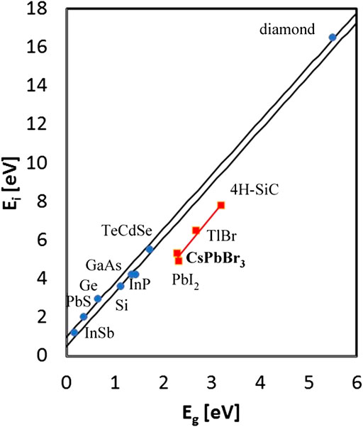
FIGURE 1. Mean energy value required to create an e–h pair in several semiconductor materials. The two solid lines evidence the range of applicability of the Klein’s empirical rules. The halide perovksite under study in this work is part of a group of materials not following this rule.
The relatively high mass density, 4.55 g/cm3 combined with the low mean ionization energy, results in a sensitivity per unit volume for CsPbBr3,
Further, other arguments in favor of using CsPbBr3 in real-time radiation monitoring applications are as follows:
CsPbBr3 is characterized by easy deposition methods, allowing to deposit on almost any kind of substrates nanostructures, single crystals and polycrystalline thin films [14];
the material is potentially defect tolerant and less prone to mid-gap states as conventional semiconductors such as Si, GaAs, and InP, since main defects in CsPbBr3 are mostly related to shallow and intra-band levels [15];
besides promising transport properties as high diffusion lengths and high charge carrier mobilities [16], CsPbBr3 has a relatively high bandgap so that it can be considered intrinsically “radiation resistant” as a particle detector. In fact, defect-assisted thermal generation of electron–hole pairs, usually originating noise in a radiation detector, should be in principle negligible at room temperature, even after very high accumulated doses [17].
This work reports on first characterizations of crystalline CsPbBr3 as dosimeters for clinical radiotherapy. In-house manufactured devices have been tested under 6 MV X-ray beams with dose and dose rates in the range of typical interest for clinical applications, in view to test the feasibility of high spatial resolution point dosimeters which could be used as pixel elements in linear and bidimensional arrays. Point dosimeters with 0.4 mm linear size have been manufactured to achieve spatial resolutions in bidimensional mapping below 1 mm. Linearity of response with the absorbed dose and the dosimetric sensitivity is evaluated. Active volume and sensitivity per unit surface are then compared with those obtained in previous works using similar samples produced as drop-casted films.
Experimental Procedure
Crystalline CsPbBr3 samples have been grown using a solvent/anti-solvent procedure, starting from a saturated solution of the CsBr and PbBr2 1:1 molar ratio in dimethyl sulfoxide. Details on the growth method are given in [18, 19]. Figure 2B shows the set of millimeter-sized crystalline CsPbBr3 samples used in this study. Optical microscope photographs evidencing the polycrystalline structure of the samples, composed by crystallites with different orientations and variable dimensions, up to about 200 μm linear size, are shown in Figure 2C. More details on the crystalline quality of the samples are reported elsewhere [18]. Details on a full sample characterization by scanning electron microscope (SEM), X-ray diffraction (XRD), and photoluminescence (PL) spectroscopy under continuous wave and picosecond excitation in the temperature range 10–300 K to assess the quality of the material can be found in Ref. [20].
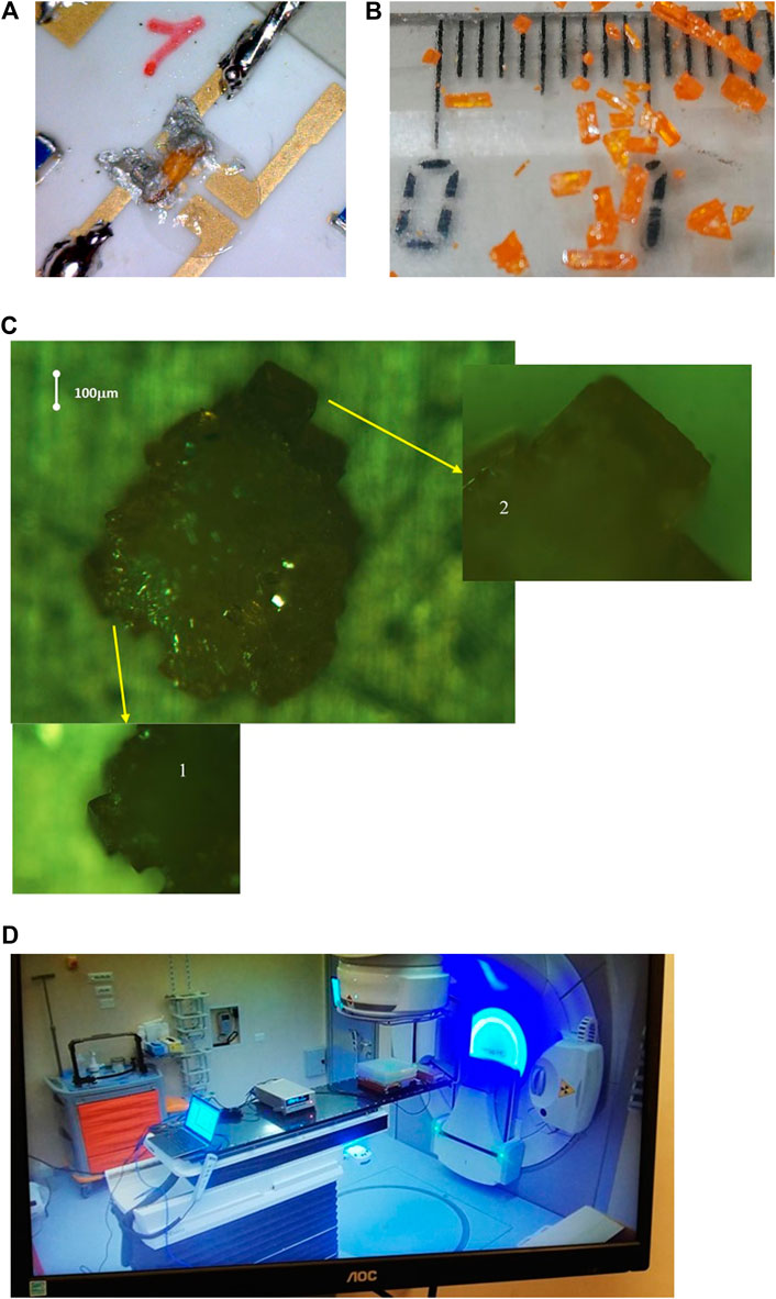
FIGURE 2. (A) A crystalline CsPbBr3 sample mounted on the alumina PCB equipped with Au contacts. (B) Photograph of the set of millimeter-sized crystalline CsPbBr3 samples used in this study; (C) Optical microscope photographs evidencing the polycrystalline structure of our samples. Crystallites with dimensions up to about 100 µm linear size are visible in insets 1 and 2; (D) The perovskite dosimetric system running under the X-ray beam within the treatment room at Dipartimento di Scienze Biomediche Sperimentali e Cliniche “Mario Serio,” Universitá di Firenze, Italy.
To produce point dosimeters, crystalline grains have been glued with silver paint in between Au planar contacts deposited on alumina printed circuit boards (PCBs). Electrode distance is 0.4 mm, and crystal surface area normal to the beam is about 0.16 mm2. The crystalline sample mounted on the PCB is then covered with PolyMethylMethAcrylate (PMMA) to prevent deterioration due to air and water vapor exposure [20]. Figure 2A shows a photograph of a crystalline sample mounted on an alumina PCB equipped with Au contacts, covered with PMMA [21].
To perform the dosimetric characterization, the device is placed within a PMMA finger inserted into a solid water phantom, positioned under the linac head at 100 cm from the source, kept under 10 cm depth of water equivalent phantom (PMMA, solid water) in view to achieve charge particle equilibrium conditions. The beam size is 10 cm x 10 cm to provide field uniformity without penumbra effects on the device which is placed on the central axis. The device is connected to a Keithley 6517A for current readout and voltage source supply remotely driven during irradiation by PC with MATLAB software. Electron read-out integrating times are in the range 10–40 ms. Figure 2D shows the device ready for dosimetric tests within the treatment room at Radiotherapy Section of Dipartimento di Scienze Biomediche Sperimentali e Cliniche “Mario Serio,” Università di Firenze, Italy.
Prior irradiation, we measured the dark current–voltage (IV) characteristics of the device mounted in the finger. After applying an external voltage across the electrodes, we waited a few minutes to achieve current stabilization [22, 23]. We used voltages in the range of ±1 V, to keep a sufficiently low electric field within the material. In fact, recent studies on CsPbBr3 samples [23] showed that, if a high electric field is applied to crystals, defect proliferation phenomena, originating from ion migration, may take place. The resulting IV characteristics are shown in Figure 3. Within our measurement errors, evaluated, respectively, ±3 pA and ±50 mV in these operative conditions, data can be interpreted considering an ohmic regime, with room temperature resistivity of about 0.8 GΩcm.
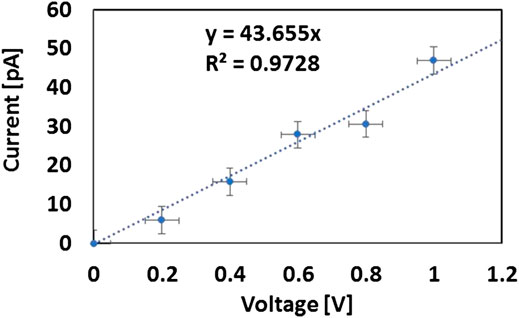
FIGURE 3. I-V characteristics in dark of a crystalline CsPbBr3 device measured as a function of applied voltage (T = 290 K) evidencing ohmic regime.
Experimental Results and Discussion
To calibrate our crystalline perovskite dosimeters, charge and current signals have been measured under conventional 6 MV X-photon beams from a linac, in a uniform 10 × 10 cm2 radiation field. The device is kept at room temperature, and a constant voltage of 1V has been applied across electrodes. To favor current stabilization, we started each measurement a few minutes after bias application. A first irradiation cycle is performed in order to “prime” the device, namely, to let traps present in the material to capture charges and then to passivate [18]. In general, a dose of about 1–3 Gy is required, depending on the samples. Then, the current signal, background subtracted, appears to be reproducible when using the same doses and dose rates. As an example, in Figure 4A, we show the current signal measured when two successive radiation pulses, each corresponding to a dose of 500cGy, are delivered under a constant dose rate (8.34 Gy/min). The current signal measured when the beam is switched on is quite similar for the two radiation pulses. In fact, current signals appear to be reproducible, as evidenced by the plot of Figure 4B, where the two signals are aligned with the same onset times. Moreover, current signals are characterized by fast decay and rise times, of the order of 1s, with the absence of transients due to polarization effects or persistent currents. The linac pulse repetition frequencies (PRF) are in the range 50–400 Hz and our read-out electronics is integrating the signal on a time frame of 10 ms, measuring the current signal under about a 4-Hz rate. In these conditions, we are not actually able to evaluate the slew rate of the sensor (in future, we plan to refine our timing measurements by means of a trans-impedance front end).
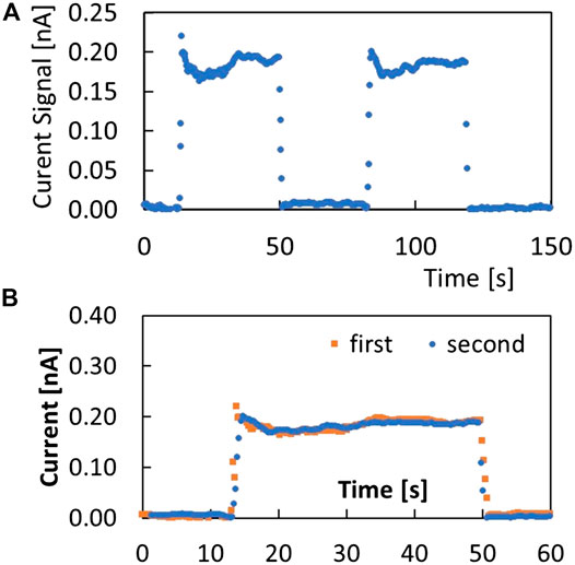
FIGURE 4. (A) Current signal of a crystalline perovskite dosimeter measured with 1V bias under a 6-MV photon beam from linac, 8.34 Gy/min constant dose rate: two successive radiation pulses, 5Gy each. (B) Comparison of the two signal responses with the same onset times.
The dosimetric response as a function of the dose has been studied measuring the current signal of our devices under an X-ray beam with a constant dose rate and increasing exposure times, to cover a dose range from 5cGy to 10Gy. Figure 5A shows the current signal (after background subtraction) measured with one CsPbBr3 device during a cycle of seven successive 6 MV photon beam irradiation pulses with Dr = 2.58 Gy/min. The complex structure of the signal for different time elongations is evidenced in Figure 5B, where pulses corresponding to different doses have been aligned in order to have the same onset times. Current instability observed in Figures 4, 5 is probably due to priming of defects which are capturing/releasing defects, activating especially at the early stage of each irradiation step. Anyway, the plot highlights how all current signals follow the same pattern, developing with the same function with time when increasing the pulse duration. Concerning the measured rise and decay times, they can be considered fast, when using conventional beams where relevant delivery times are of the order or higher than 1s.
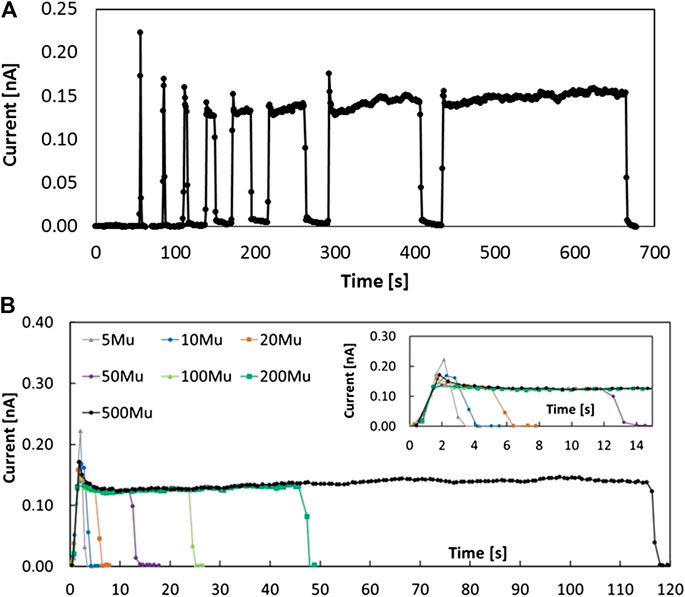
FIGURE 5. Dosimetric test results of a crystalline perovskite dosimeter under linac 6 MV X-photon beam irradiation at the same dose rate, 2.58 Mu/min, when 1V external voltage is applied across the sample. (A) Current signal as a function of time for seven successive pulses and increasing duration; (B) comparison of current signals with the same onset times for different doses, in the range up to 500Mu. Inset highlights the shorter pulses.
The charge response at different doses is measured as the integral of the current response during each irradiation pulse, after subtraction of the extrapolated background current. The plot of the collected charge as a function of the dose is shown in Figure 6A. Results evidence the linear dependence of the collected charge on the absorbed dose. We observe that the current instability measured during irradiation is not influencing the dose calculated by current signal integration at each delivery step. This can be explained considering that active defects are capturing and releasing charged carriers within the time window of the dose delivery itself; thus, they are not affecting the dose calculation. To determine the sensitivity of our device, data have been best-fitted to a line: slope value is S = 3.4 nC/Gy. To be able to work with modern radiotherapy machines, as VMAT, where dose rates are continuously varying during treatments, a dosimetric device should be characterized also by a linear dependence of the current signal on the dose rate. The current signal measured with another device (same material, and same voltage applied and contact geometry) under four different dose rates in the range 30–530 Mu/min (X6MV photon beam) is plotted as a function of the dose rate in Figure 6B.
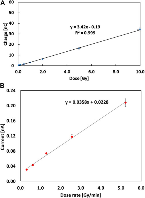
FIGURE 6. (A) Charge signal measured with one crystalline perovskite dosimeter when 1V applied external voltage under X photon beam from linac: charge as a function of dose for the same dose rate, 258 Mu/min in case of 6 MeV highest energy. Best fit to data evidences a linear behavior of charge with dose. (B) Current signal as a function of dose rate measured with a different crystalline perovskite dosimeter when applied a 1V external voltage under X6MV photon beam from linac. Best fit of data of figures evidence linear behavior.
From the sensitivity S value determined by our charge vs dose measurements, it is possible to get a first evaluation of the charge collection distance, ccd, namely, the average distance the e–h pairs created by radiation can travel in our samples before they are recombined at a defect. Starting from the known theoretical value of the sensitivity per unit volume, SV = 860 nC/(Gy mm3), considering our sample as a cube with size 0.4 mm, we estimate:
Finally, we observe that first results obtained with crystalline CsPbBr3 dosimeters compare favorably with those previously obtained with drop-casted CsPbBr3 thin films deposited on similar PCBs [6]. This holds in particular for the sensitivity per unit surface for crystalline devices, about 22 nC/(Gy mm2), much higher than 1.4 nC/(Gy mm2), the value measured with drop-casted CsPbBr3 thin films [6]. As a consequence of this increased sensitivity per unit surface, crystalline CsPbBr3 can act as point dosimeters with linear dimensions well below 1 mm, so matching the ultimate constraint for spatial resolution in bidimensional mapping of the dose in clinical radiotherapy.
Conclusion
Lead halide perovskite CsPbBr3 is a wide-gap semiconductor material potentially very attractive for next generations of real-time dosimeters and possibly for future particle detectors in high-energy physics. This work reports on first experimental results concerning crystalline CsPbBr3 samples. First submillimeter point dosimeters have been produced and tested with a high-energy X-photon beam used for clinical radiotherapy applications. First results reported here are promising in terms of fast rise and decay times, absence of polarization effects during irradiation, reproducibility of the current signal in repeated pulses, and linearity of the collected charge as a function of the absorbed dose. If we compare the measured sensitivity with the theoretical one, we estimate a charge collection distance ccd of about 100 μm, a value of the same order of the linear dimensions of the crystallites composing the material. This suggests that recombination centers responsible for incomplete charge collection may be placed at grain boundaries. If so, crystalline samples should be less subjected to the detrimental effects due to defects then drop-casted samples, composed by grains of only a few micron size [6, 18]. In order to further increase the sensitivity per unit volume of our devices, in future, a more efficient charge collection should be achieved, for example, by further increasing the linear dimension of the crystallites and their orientation through the sample. This can be, in principle, performed by a detailed control of the growth process parameters [24]; this will be the subject of a forthcoming work.
Finally, we observe that the crystalline samples tested in this work are characterized by a much higher sensitivity per unit area than that of drop-casted CsPbBr3 thin films. This opens the way to CsPbBr3 point dosimeters with linear dimensions below 1mm, well matching the strict spatial resolution constraints in bidimensional dose mapping required in clinical radiotherapy. In future, we plan to perform studies with the same devices under IMRT and VMAT beams. To this purpose, the read-out electronics will be optimized to evaluate correctly even doses delivered with times lower than 1s. Further, we are planning to measure output factors, namely, the response of the device under beams of decreased size, to study the effect of the profile of a collimated x-ray beam on the dosimetric response of the device.
Data Availability Statement
The raw data supporting the conclusions of this article will be made available by the authors, without undue reservation.
Author Contributions
Conceptualization, MB and CT; methodology, MB and CT; software, MB; device manufacturing, MB; validation, MB and CT; formal analysis, MB; investigation, MB and CT; resources, MB and CT; data curation, MB and CT; writing—original draft preparation, MB; writing—review and editing, MB and CT; supervision, MB; project administration, MB; and funding acquisition, MB.
Funding
This work was performed in the framework of the experiment PERO2 financed by Istituto Nazionale di Fisica Nucleare, CSN5-INFN, Italy.
Conflict of Interest
The authors declare that the research was conducted in the absence of any commercial or financial relationships that could be construed as a potential conflict of interest.
Acknowledgments
The authors warmly thank N. Calisi and S. Caporali of Università di Firenze, Dipartimento di Ingegneria Industriale, Via S. Marta 3, 50139 Firenze, Italy, for having provided the crystalline CsPbBr3 samples. They also wish to thank Anna Vinattieri and Naomi Falsini of Università di Firenze, Dipartimento di Fisica e Astronomia, Via G. Sansone 1, 50019 Sesto Fiorentino (FI), Italy, for useful discussions about material characterization.
References
1. Tsai H, Liu F, Shrestha S, Fernando K, Tretiak S, Scott B, et al. A sensitive and robust thin-film x-ray detector using 2D layered perovskite diodes. Sci Adv (2020) 6(15):815. doi:10.1126/sciadv.aay0815
2. Saidaminov MI, Adinolfi V, Comin R, Abdelhady AL, Peng W, Dursun I, et al. Planar-integrated single-crystalline perovskite photodetectors. Nat Commun (2015) 6:8724. doi:10.1038/ncomms9724
3. Pierre A, Deckman I, Lechêne PB, Arias AC. High detectivity all-printed organic photodiodes. Adv Mater (2015) 27(41):6411–7. doi:10.1002/adma.201502238
4. Kim YC, Kim KH, Son DY, Jeong DN, Seo JY, Choi YS, et al. Printable organometallic perovskite enables large-area, low-dose X-ray imaging. Nature (2017) 550(7674):87–91. doi:10.1038/nature24032
5. Gill HS, Elshahat B, Kokil A, Li L, Mosurkal R. Flexible perovskite based X-ray detectors for dose monitoring in medical imaging applications. Phys Med (2018) 5:20. doi:10.1016/j.phmed.2018.04.001
6. Bruzzi M, Talamonti C, Calisi N, Caporali S, Vinattieri A. First proof-of-principle of inorganic perovskites clinical radiotherapy dosimeters. Appl Phys Lett Mat (2019) 7:051101. doi:10.3390/nano10010060
7. Stoumpos CC, Malliakas CD, Peters JA, Liu Z, Sebastian M, Im MJ, et al. Crystal growth of the perovskite semiconductor CsPbBr3: a new material for high-energy radiation detection. Cryst Growth Des (2013) 13 2722–7.
8. Allison RR, Sibata C, Patel R. Future radiation therapy: photons, protons and particles. Future Oncol (2013) 9:493–504. doi:10.2217/fon.13.13
9. Bruzzi M. Novel silicon devices for radiation therapy monitoring. Nucl Instrum Methods Phys Res Sect A (2016) 809:105. doi:10.1016/j.nima.2015.10.072
10. Klein CA. Bandgap dependence and related features of radiation ionization energies in semiconductors. J Appl Phys (1968) 39:2029. doi:10.1063/1.1656484
11. Yihui H, Matei L, Jung HJ, McCall KM, Chen M, Stoumpos CC, et al. High spectral resolution of gamma-rays at room temperature by perovskite CsPbBr3 single crystals. Nat Commun (2018) 9:1609. doi:10.1038/s41467-018-04073-3
12. Shah KS, Lund JC, Olschner G, Moy L, Squillante MR. Thallium bromide radiation detectors. IEEE Trans Nucl Sci (1989) 36:199–202. doi:10.1109/23.34434
13. Owens A, Peacock A. Compound semiconductor radiation detectors. Nucl Instrum Methods Phys Res A (2004) 531:18–37. doi:10.1016/j.nima.2004.05.071
14. Seth S, Samanta A. A facile methodology for engineering the morphology of CsPbX3 perovskite nanocrystals under ambient condition. Sci Rep (2016) 6:37693. doi:10.1038/srep37693
15. Kovalenko MV, Protesescu L, Bodnarchuk MI. Properties and potential optoelectronic applications of lead halide perovskite nanocrystals Science (2017) 358:745–50. doi:10.1126/science.aam7093
16. Motta C, El-Mellouhi F, Sanvito S. Charge carrier mobility in hybrid halide perovskites. Sci Rep (2014) 5:12746. doi:10.1038/srep12746
17. Bruzzi M, Sadrozinski HFW, Seiden A. Comparing radiation tolerant materials and devices for ultra rad-hard tracking detectors. Nucl Instrum Methods Phys Res A (2007) 579:754–61. doi:10.1016/j.nima.2007.05.326
18. Bruzzi M, Falsini N, Calisi N, Vinattieri A. Electrically active defects in polycrystalline and single crystal metal halide perovskite. Energies (2020) 13:1643. doi:10.3390/en13071643
19. Rakita Y, Kedem N, Gupta S, Sadhanala A, Kalchenko V, Böhm ML, et al. Low-temperature solution-grown CsPbBr3 single crystals and their characterization. Cryst Growth Des (2016) 16:5717–25.doi:10.1021/acs.cgd.6b00764
20. Gabelloni F, Biccari F, Falsini N, Calisi N, Caporali S, Vinattieri A. Long-living nonlinear behavior in CsPbBr3 carrier recombination dynamics. Nanophotonics (2019) 8:1447–55. doi:10.1515/nanoph-2019-0013
21. Calisi N, Caporali S, Milanesi A, Innocenti M, Salvietti E, Bardi U. Composition-dependent degradation of hybrid and inorganic lead perovskites in ambient conditions. Top Catal (2018) 61:1201–8.
22. Chen C, Fu Q, Guo P, Chen H, Wang M, Luo W, et al. Ionic transport characteristics of large-size CsPbBr3 single crystals. Mater Res Express (2019) 6:115808. doi:10.1088/2053-1591/ab4d79
23. Zhang BB, Wang F, Zhang H, Xiao B, Sun Q, Guo J, et al. Defect proliferation in CsPbBr3 crystal induced by ion migration. Appl Phys Lett (2020) 116:063505. doi:10.1063/1.5134108
Keywords: photodetectors, lead halide perovskite, CsPbBr3, 1D dosimeter, radiotherapy, real-time monitor system
Citation: Bruzzi M and Talamonti C (2021) Characterization of Crystalline CsPbBr3 Perovksite Dosimeters for Clinical Radiotherapy. Front. Phys. 9:625282. doi: 10.3389/fphy.2021.625282
Received: 02 November 2020; Accepted: 15 January 2021;
Published: 04 March 2021.
Edited by:
Gian-Franco Dalla Betta, University of Trento, ItalyReviewed by:
Marco Petasecca, University of Wollongong, AustraliaBruce Wessels, Northwestern University, United States
Copyright © 2021 Bruzzi and Talamonti. This is an open-access article distributed under the terms of the Creative Commons Attribution License (CC BY). The use, distribution or reproduction in other forums is permitted, provided the original author(s) and the copyright owner(s) are credited and that the original publication in this journal is cited, in accordance with accepted academic practice. No use, distribution or reproduction is permitted which does not comply with these terms.
*Correspondence: Mara Bruzzi, bWFyYS5icnV6emlAdW5pZmkuaXQ=