
95% of researchers rate our articles as excellent or good
Learn more about the work of our research integrity team to safeguard the quality of each article we publish.
Find out more
ORIGINAL RESEARCH article
Front. Phys. , 18 March 2021
Sec. Radiation Detectors and Imaging
Volume 9 - 2021 | https://doi.org/10.3389/fphy.2021.618390
This article is part of the Research Topic Advanced fabrication technologies for semiconductor radiation detectors View all 13 articles
 Julie Segal1*
 Christopher Kenney1Jeffrey M. Kowalski2
 Jeffrey E. Kowalski2Gabriel Blaj1
 Lisa Rozario1Jasmin Hasi1Angelo Dragone1Pietro Caragiulo1Lorenzo Rota1
New free electron lasers, such as SLAC’s LCLS-II, will provide unique scientific imaging opportunities. In order to fully utilize these facilities, we need to develop detectors with shallow entrance windows that will enable detection of soft x-rays from 250 eV to 1.5 KeV. Achieving adequately shallow entrance windows is challenging because the high temperature anneal needed to activate the dopant also drives the dopant profile deeper, growing the region that is insensitive to soft x-rays. A new microwave annealing technology provides an efficient way to achieve shallow entrance windows in fully depleted high-resistivity silicon sensors. The microwave anneal technique can activate dopants at low substrate temperature, with minimal dopant diffusion, and can be used to fabricate both n-type and p-type entrance windows. SRP and SIMS measurements were used to verify dopant activation with negligible dopant diffusion. We then applied the microwave anneal process to a planar sensor wafer, using the new process to create the backside diode contact. Electrical test of the resulting sensors shows good reverse bias characteristics. The sensors have been bump-bonded to a read-out ASIC and used successfully to measure an Fe-55 x-ray spectrum. Process and device simulations were performed to characterize the quantum efficiency of the entrance window for soft x-rays. This technique is useful for other sensor applications requiring a shallow entrance window, including detectors for UV photons, low energy ions and low energy electrons.
SLAC’s LCLS-II will provide unique opportunities for scientific imaging. To take advantage of this potential we need to develop detectors for soft x-rays from 250 eV to 1.5 KeV. Our challenge is to develop detectors with adequately low noise to resolve these energies, and with shallow entrance windows to avoid absorbing the x-rays in the insensitive region of the sensor [1–3]. Other free electron laser facilities in Germany, China, Korea, Japan, and Switzerland as well as synchrotrons would also benefit from a low-cost, reliable method for forming shallow entrance windows.
Fully depleted high resistivity silicon sensors require a highly doped region at the entrance window to terminate and contact the diode. Typically, this region is created by ion implantation of the dopant species, followed by a high temperature anneal to activate the dopant. This anneal also drives the dopant profile deeper, increasing the entrance window depth and limiting sensitivity to soft x-rays. The available solutions, such as laser annealing, are very expensive and difficult to implement in volume manufacturing.
Microwave annealing (MWA) has the potential to be an efficient, cost effective way to achieve shallow entrance windows in silicon sensors. The dopants become polarized in the microwave chamber, allowing for dopant activation while the bulk silicon temperature remains at less than 500°C. The result is dopant activation with negligible dopant diffusion [3–6].
To support a range of sensor applications that includes both hole-collecting and electron-collecting silicon sensors, we need a solution that applies to both n-type and p-type entrance windows. We applied the microwave anneal process to test wafers implanted with Arsenic, Phosphorus, Boron, and BF2. Arsenic and BF2 have shallower implant profiles, making them the most promising options for shallow entrance windows. The implant conditions are shown in Table 1. The microwave anneal step was performed with DSG Technologies’ Axom tool.
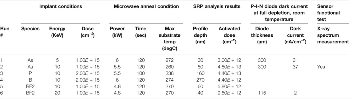
TABLE 1. Microwave annealed dopant profiles results. Implant parameters and microwave anneal conditions for our experiments, with SRP results and, where available, dark current results.
A secondary ion mass spectrometry (SIMS) profile was acquired to determine the dopant distribution for run #2 (10 KeV Arsenic implant) after microwave anneal. The result was compared with a simulated as-implanted profile in Figure 1. The dopant profile did not shift significantly compared to the expected as-implanted profile, indicating negligible dopant diffusion.
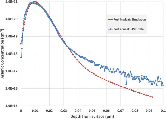
FIGURE 1. Profile for 10 KeV Arsenic implant: process simulation of post-implanted profile, and experimental results (SIMS data) for the same implant after microwave anneal.
Spreading resistance profile (SRP) measurements were acquired to characterize the activated dopant profiles, with approximate profile depth (defined as depth where implanted dopant concentration drops to 1014 cm−3) and activated dopant levels (based on integrated carrier concentration) shown in Table 1. The shallow profile depth confirms the conclusion that there was negligible dopant diffusion during the anneal. In our initial experiments, the activated dose was only a small fraction of the implanted dose. In the case of the 5 KeV Arsenic implant less than 1/100th of the dose was activated. The low activation level for the 5 KeV Arsenic implant compared to the 10 KeV implant may be due to the lower implant energy causing less lattice damage, because the activation occurs in part when then dopant is incorporated into the lattice during re-crystallization [5]. We expect that further co-optimization of the implant and microwave anneal processes will improve the dopant activation level.
For our sensor application the low dopant activation levels are adequate, because we only need enough dopant to terminate the P-intrinsic-N (P-I-N) diode structure. For 300 V over-bias above depletion voltage on a 300 μm thick sensor, 6.4 × 1010 cm−2 is the minimum active dose.
Arsenic entrance windows were applied to P-I-N diode sensor wafers fabricated at the Stanford Nanofabrication Facility (SNF) [3]. Our in-house built sensors are processed on 300 um thick n-type high resistivity float-zone silicon, with p-type diffusion on the front side (Figures 2, 3). Thick metal (0.5 μm) is patterned around the edge of the entrance window for electrical contact, and a thin metal layer (10 nm) was deposited on the entrance window to block unwanted light. In order to ensure that the microwave annealed dopant profile terminates the P-I-N diode without defects and without damage to the silicon lattice, area-based dark currents were measured at room temperature. Dark current results, shown in Table 1 and Figure 4, are comparable to measurements on similar structures terminated with conventionally annealed implants. Full depletion was reached at approximately 40 V, with no breakdown occurring at diode bias up to 200 V.
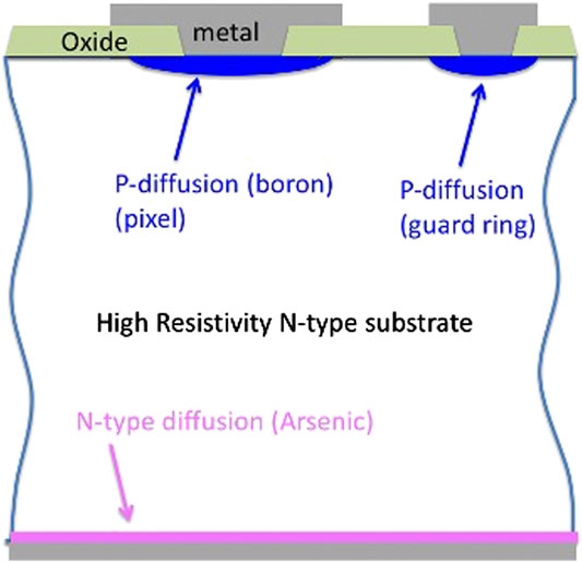
FIGURE 2. Schematic cross-section of SLAC in-house planar sensor process. The n-type Arsenic profile constitutes the entrance window.
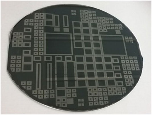
FIGURE 3. SLAC planar sensor wafer processed at the Stanford Nanofabrication Facility (SNF). The entrance window with patterned metal is shown.
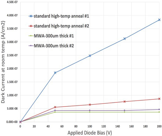
FIGURE 4. Dark current measured on PIN diodes test structures with conventional anneal and microwave anneal. The microwave annealed sensors have comparable dark current based on this small sample of typical devices.
We deployed several small proto-type size (96 × 96 pixels) sensors with 50 μm pixel pitch from our planar sensor wafers with microwave annealed arsenic entrance windows. The sensors were bump-bonded to the ePix100 read-out ASICs [7,8]. The resulting camera is shown in Figure 5. We tested the proto-type with an Fe-55 x-ray source, and successfully obtained the spectrum shown in Figure 6. From these results we can conclude that the microwave anneal process is compatible with high resistivity silicon detector processing. Future work will involve testing the system with soft x-rays to experimentally verify the shallow entrance window.
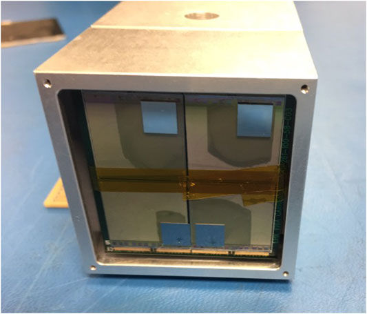
FIGURE 5. Camera assembled with prototype shallow entrance window sensors bump-bonded to SLAC ePix100 read-out ASIC.

FIGURE 6. Fe-55 spectrum (shown in blue) measured on planar sensor with microwave annealed entrance window bump-bonded to ePix100 ASIC. Results are comparable to measurements taken with conventional sensors.
We performed TCAD process and device simulations to understand the physics of entrance windows with very shallow dopant profiles, and to characterize the quantum efficiency of these structures for soft x-ray photons.
The baseline simulation structure is a 300 um thick P-I-N diode fabricated on 4.3 K ohm cm n-type silicon, illustrated in Figure 7. For these simulations, we focused on a hole-collecting sensor configuration with an n-type entrance window. However, the results are expected to be similar for the reverse configuration with equivalent p-type entrance window profiles. We used Synopsys Sentaurus process and device simulation tools. We performed a full 3D simulation in order to accurately model the charge cloud evolution and drift. All default parameters were used, with the exception of minority carrier lifetime which was set at 1 mS to reflect the use of float-zone silicon used for high resistivity sensors.
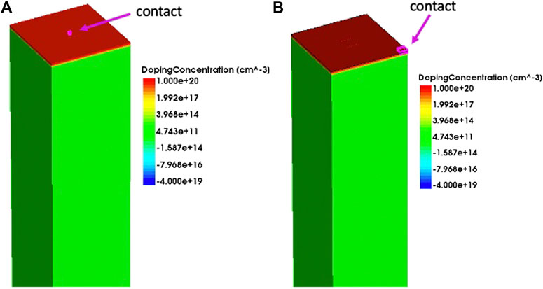
FIGURE 7. PIN diode structure used for TCAD simulations of x-ray charge collection. (A)(left) has a contact (shown in pink) in the center, where the simulated photon is absorbed. (B) right has an oxide interface over the simulated photon absorption location, with an electrical contact (pink square) in the corner.
We simulated four n-type different dopant profiles: 1) 5 KeV Arsenic implant, based on the SRP results for run #1 in Table 1, 2) 10 KeV Arsenic implant, based on the SRP results run #2 in Table 1, 3) Simulated 20 KeV Arsenic implant with a 900 deg 30 min conventional anneal, resulting in a 0.2 μm deep profile, and 4) A 2 μm deep profile, which could be achieved with a phosphorus implant and long high-temperature anneal. The four profiles are shown in Figure 8. During the first round of simulations, the electrode was defined in the center of the entrance window where the photon absorption is simulated, as shown in Figure 7A. The electrode behaves electrically like a metal contact.
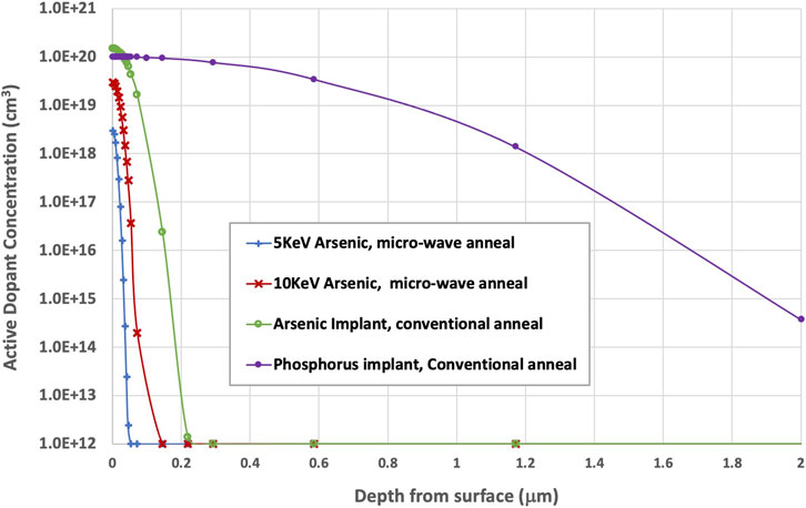
FIGURE 8. Activated dopant profiles for four entrance window profiles simulated for this work. The spacing of the data points reflects the grid spacing in the vertical direction, which is about 5 nm for the first 50 nm from the surface.
A simulated bias of 100 V was applied to all four structures. The resulting electric field near the entrance window is shown in Figure 9A. Note that for all of the dopant profiles, with the exception of the deepest, there is significant electric field present all the way to the surface. This can be understood from examining the electron density, shown in Figure 9B. For the deepest profile, the n-type dopant profile is mostly undepleted, and the electron density is similar to the activated dopant density in Figure 8. In the case of the shallower three profiles, however, the steep impurity gradient result in the electric field near the surface. In general, a graded impurity distribution in silicon causes a built-in electric field due to carrier diffusion along the gradient [9]. This effect becomes important when the gradient is large, as we can see by comparing the electron distribution in Figure 9B to the activated n-type dopant distribution in Figure 8.
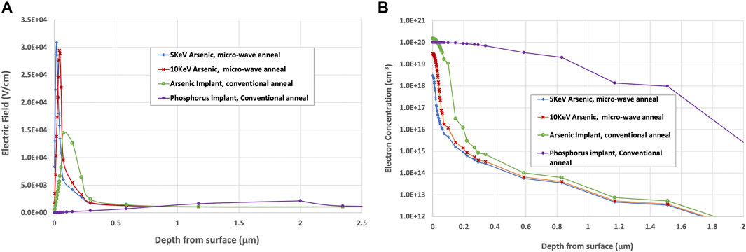
FIGURE 9. With simulated applied bias of 100 V (A) Electric field near entrance window, and (B) electron density near entrance window. These results are the same for the center and corner contact versions of the simulation.
In order to simulate the absorption of photons, electron-hole pair clouds were placed at various distances from the interface at the center of the entrance face using the heavy ion model, as illustrated in Figure 10. The resulting readout signal was studied. The total integrated read-out current was compared to the initial charge that was deposited in the substrate. The results are shown in Figure 11A. The percentage of the charge that gets collected decreases dramatically for photons absorbed near the surface, despite the presence of a significant electric field shown in Figure 9A. We can understand this mechanism by comparing structure in Figures 7A,B. We added oxide to the surface of the structure in Figure 7B and moved the electrical contact to the corner, away from the photon absorption region. We see the impact of this change comparing Figures 11A,B. In Figure 11B, with an oxide interface instead of a metallic electrode, greater than 90% of the charge packet is collected for three of the four entrance window designs. The difference is the surface recombination velocity of the metal contact (approximately 106 cm s−1) compared to oxide interface (103 cm s−1). (Default surface recombination velocity parameters from Sentaurus Synopsis were used.) With shallow absorption, holes diffuse to the surface and recombine at the metal contact interface, instead of being swept away from the interface by the electric field. On the other hand, with the oxide interface surface recombination is negligible, and only the deepest dopant profile, with a significant zero-field region, results in enough bulk recombination to diminish the signal collection.
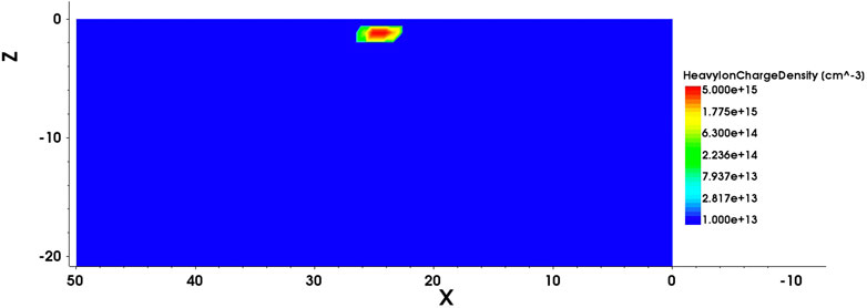
FIGURE 10. Illustration of photon absorption simulation, showing charge cloud initiated 1 mm (1000 μm) from the entrance window surface.
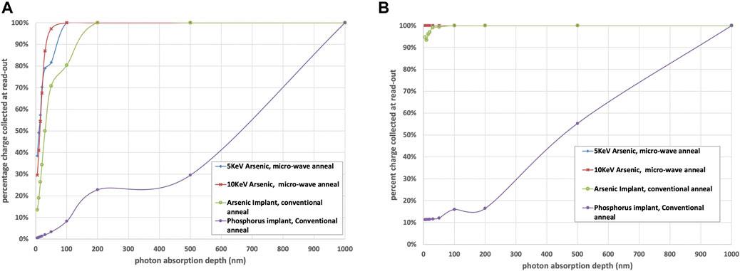
FIGURE 11. Simulated charge read-out vs. photon absorption depth in silicon for (A) metal contacted entrance window, and (B) oxide interface. Figures show percentage of generated charge that is collected at read-out node.
Note that the actual surface recombination velocity at the oxide-silicon interface is highly process dependent [10,11]. In practice, the sensor process requirements and limits on x-ray blocking insulator thickness may constrain process options. Our objective for these simulations is to understand how electric field distribution at the entrance window and surface recombination interact to control the quantum efficiency for soft x-rays.
A further observation from Figure 11A is that the percentage charge read-out for photons absorbed between 30 and 100 nm is higher for the 10 KeV Arsenic implant than for the 5 KeV implant, despite the fact the 5 KeV implant results in a shallow profile. This is likely due to the fact that the electric field in this region is higher for the 10 KeV implant, as seen in Figure 9A, which speeds up the separation of the electrons and holes and moves the holes away from the interface. Similarly, the arsenic junction with conventional annealing is about 200 nm deep in Figure 8, but the collection is signification at 100 nm and below in Figure 11. This can again be understood from Figure 9A, showing the electric field actually peaks around 100 nm.
In general, the electric field profile determines the functional entrance window. For traditional diffused junctions, which are deeper with more gently graded profiles, the electric field is very low in the doped region. For shallow, steep profiles the electric field may be quite high in the doped region. In any case, we need to look at the electric field profile to understand the entrance window performance.
Based on the simulation results in Figures 11A,B and standard models for absorption of photons in silicon, we calculated the quantum efficiency for four photon energies of interest: 250, 619, 930 and 1500 eV. The results for our four entrance window structures are shown in Figure 12A for metal contact, and Figure 12B for oxide interface. Note that these results do not take into account any losses through metal or oxide films. Also note that the actual quantum efficiency of a detector system will depend on the read-out technique and other factors, such whether the amplifier will register a fractional read-out, and signal to noise ratio. Nevertheless, these results are useful for understanding how the shallow dopant profiles that are achievable with microwave annealing may affect sensor quantum efficiency. For these structures, bulk recombination in the undepleted window region is not responsible for signal loss in our simulations. Instead, the surface treatment will become the dominant concern.
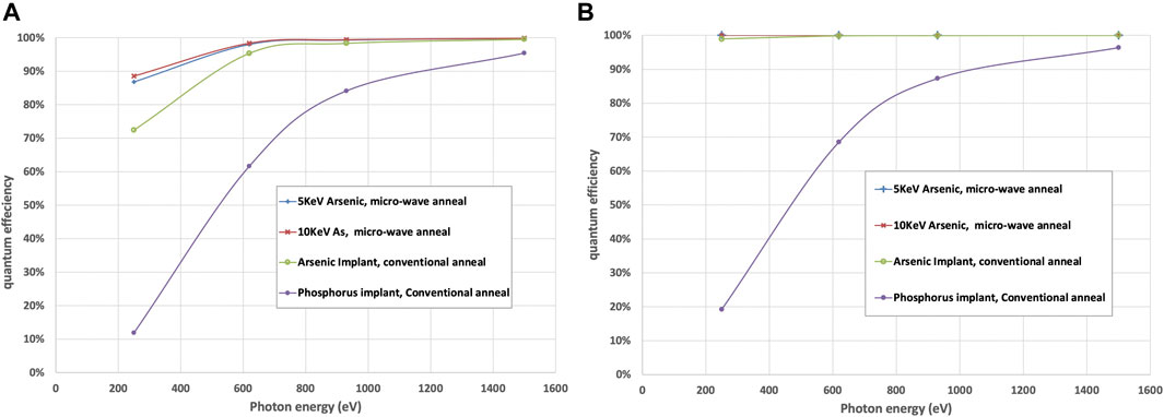
FIGURE 12. Simulated quantum efficiency for entrance window with (A) metal contacted entrance window, and (B) oxide interface for 250, 619, 930 and 1500 eV photons, based on percentage absorption shown in Figure 10. Losses from photon absorption in metal or oxide layers are not included in the calculations.
We have demonstrated a new technology, microwave annealing, with the potential to enable simple, low cost processing of shallow entrance windows for high resistivity silicon soft x-ray sensors. The new entrance window process has been successfully applied to high resistivity silicon sensors and deployed for x-ray detection. TCAD simulations have been performed to understand the quantum efficiency for the resulting shallow dopant profiles.
Spreading resistance profile measurements of dopant activation, dark current results, and x-ray spectrum results all point to a high-quality sensor with a very shallow entrance window. However, we have not yet tested the quantum efficiency of our structure for soft x-rays. It is possible that un-annealed silicon damage from the implant or the presence of un-activated dopant will affect the sensitivity of the sensor near the entrance window. Further measurements will be required to resolve this issue.
In addition to providing a shallow junction, microwave annealing for sensor dopant activation can add flexibility to the process integration. Because the substrate is not heated during the anneal, the technique can be used to post-process the backside of fully depleted monolithic CMOS sensors and CCD’s, significantly simplifying the process [4].
Finally, this technique may prove useful for other sensor applications requiring shallow entrance windows, including detectors for UV photons, low energy ions and low energy electrons.
The raw data supporting the conclusions of this article will be made available by the authors, without undue reservation.
JS and CK conceived the idea for this work and planned and evaluated experiments. JS also performed TCAD simulations and prepared the manuscript. JMK and JEK developed and executed the microwave anneal process. LIR and JH performed wafer processing and bump bonding. GB assembled camera and ran and analyzed tests to obtain x-ray spectrum. AD an PC are responsible for the design and development of the read-out ASIC used to obtain x-ray spectrum. LOR was responsible for test structure design.
This work was supported in part by the U.S. Department of Energy under Contract No. DE-AC02-76SF00515. Work was performed in part in the nano@Stanford labs, which are supported by the National Science Foundation as part of the National Nanotechnology Coordinated Infrastructure under award ECCS-2026822. Additional funding provided by DOE Basic Energy Science (BES) program and DOE High Energy Physics (HEP) program.
Authors JMK and JEK were employed by DSG Technologies.
The remaining authors declare that the research was conducted in the absence of any commercial or financial relationships that could be construed as a potential conflict of interest.
1. Hartmann R, Strüder L, Kemmer J, Lechner P, Fries O, Lorenz E, et al. Ultrathin entrance windows for silicon drift detectors. Nucl Instrum Methods A (1997) 387:250–4. doi:10.1016/s0168-9002(96)01000-5
2. Rota L, Tamma C, Segal JD, Caragiulo P, Kenney C, Dragone A. Design of ePixM, a fully-depleted monolithic CMOS active pixel sensor for soft X-ray experiments at LCLS-II. JINST (2019) 14(12):C12014. doi:10.1088/1748-0221/14/12/c12014
3. Segal JD, Kenney CJ, Rozario L, Blaj G, Chang CE, Hasi J, et al. Thin-entrance window sensors for soft X-rays at LCLS-II. In: IEEE nuclear science symposium and medical imaging conference proceedings (NSS/MIC); 2018 Nov 10–17; Sydney, Australia. Sydney, Australia: IEEE (2018). p. 1–2. doi:10.1109/NSSMIC.2018.8824674
4. Segal JD, Kenney CJ, Rozario L, Blaj G, Chang CE, Hasi J, et al. Low-temperature junction formation for thinned high energy physics sensors. In: IEEE nuclear science symposium and medical imaging conference proceedings (NSS/MIC); 2018 Nov 10–17; Sydney, Australia. Sydney, Australia: IEEE (2018). p. 1–2. doi:10.1109/NSSMIC.2018.8824728
5. Kowalski JM, Kowalski JE, Lojek B. Microwave annealing for low temperature activation of as in Si. In: 15th international conference on advanced thermal processing of semiconductors; 2007 Oct 2; Sicily, Catania. IEEE (2007). p. 51–6. doi:10.1109/RTP.2007.4383818
6. Lee YJ, Hsueh FK, Huang SC, Kowalski JM, Kowalski JE, Cheng AT, et al. A low-temperature microwave anneal process for boron-doped ultrathin Ge epilayer on Si substrate. IEEE Electron Device Lett (2009) 30(2):123–125. doi:10.1109/led.2008.2009474
7. Dragone A, Caragiulo P, Markovic B, Herbst R, Reese B, Herrmann SC, et al. ePix: a class of architectures for second generation LCLS cameras. J Phys Conf (2014) 493:012012. doi:10.1088/1742-6596/493/1/012012
8. Blaj G, Caragiulo P, Dragone A, Haller G, Hasi J, Kenney CJ, et al. X-ray imaging with ePix100a: a high-speed, high-resolution, low noise camera. In: SPIE proceedings, hard x-ray, gamma-ray and neutron detector physics XVIII; 2016 Sep 30; Bellingham, WA. Bellingham, WA: SPIE (2016) 9968. p. 99680J
9. Muller RS, Kamins TI. Device electronics for integrated circuits. 2nd ed. New York: John Wiley and Sons (1986). 168–73.
10. Cuevas A, Basore PA, Giroult‐Matlakowski G, Dubois C. Surface recombination velocity of highly doped n-type silicon. J Appl Phys (1996) 80(6):3370–5. doi:10.1063/1.363250
Keywords: silicon sensors, x-ray sensors, micro-wave anneal, soft x-rays, silicon processing
Citation: Segal J, Kenney C, Kowalski JM, Kowalski JE, Blaj G, Rozario L, Hasi J, Dragone A, Caragiulo P and Rota L (2021) Thin-Entrance Window Process for Soft X-Ray Sensors. Front. Phys. 9:618390. doi: 10.3389/fphy.2021.618390
Received: 16 October 2020; Accepted: 05 January 2021;
Published: 18 March 2021.
Edited by:
Angela Kok, Sintef Digital, NorwayReviewed by:
Carlo Fiorini, Politecnico di Milano, ItalyCopyright © 2021 Segal, Kenney, Kowalski, Kowalski, Blaj, Rozario, Hasi, Dragone, Caragiulo and Rota. This is an open-access article distributed under the terms of the Creative Commons Attribution License (CC BY). The use, distribution or reproduction in other forums is permitted, provided the original author(s) and the copyright owner(s) are credited and that the original publication in this journal is cited, in accordance with accepted academic practice. No use, distribution or reproduction is permitted which does not comply with these terms.
*Correspondence: Julie Segal, anNlZ2FsQHNsYWMuc3RhbmZvcmQuZWR1
Disclaimer: All claims expressed in this article are solely those of the authors and do not necessarily represent those of their affiliated organizations, or those of the publisher, the editors and the reviewers. Any product that may be evaluated in this article or claim that may be made by its manufacturer is not guaranteed or endorsed by the publisher.
Research integrity at Frontiers
Learn more about the work of our research integrity team to safeguard the quality of each article we publish.