 Zeyong Wei
 Hongkun Li1,2
94% of researchers rate our articles as excellent or good
Learn more about the work of our research integrity team to safeguard the quality of each article we publish.
Find out more
ORIGINAL RESEARCH article
Front. Phys. , 29 January 2021
Sec. Optics and Photonics
Volume 8 - 2020 | https://doi.org/10.3389/fphy.2020.632902
This article is part of the Research Topic Tunable and Reconfigurable Optical Metamaterials View all 11 articles
In recent years, active metasurfaces have induced more interests, which provides great freedom of wave manipulation and gives rise to many novel phenomena. High impedance metasurfaces are a kind of artificial structures characterized by the in-phase reflection at the resonant frequency. It works as a magnetic mirror and can be applied in subwavelength cavity, low profile reflector antenna, etc. When introduce in tunable components, it possesses versatile functionalities and broader application. In this paper, we proposed an active high impedance metasurface which exhibits highly efficient absorption to the electromagnetic incidence. As an array of diodes are loaded between the gap of periodic gratings and applied with positive bias, the absorption frequency can be dynamically controlled by the level of bias voltage. At the resonant frequency, the reflection from the metasurface can be less than 1%, implying that most of the incidence is absorbed by the magnetic resonance of high impedance metasurface. When the bias voltage is tuned from 0 to +1.33 V (the forward voltage), the resonant peak rises from 8.5 to 9.1 GHz, providing a flexible control of electromagnetic wave absorption in X band.
Recently, metasurfaces [1] have attracted a great deal of attention due to their ability to freely manipulate electromagnetic waves within the sub-wavelength thickness, obtaining desirable electromagnetic properties that are not available in nature [2–5]. They have great potential for applications in microwave communication, integrated circuits, antennas, and so on [4, 6–9]. When combined with tunable mechanism, metasurfaces present variable electromagnetic properties with respect to the external condition and provide dynamic control of the incident waves [10, 11]. Metasurfaces based on tunable mechanisms such as optical [12, 13], thermal [14], electrical [15–19], and MEMS [20, 21] have been proposed to enable the dynamic control of electromagnetic waves.
High impedance surface (HIS) [22, 23]is a kind of sandwich structures comprised of periodical metallic patterns, dielectric spacer and metallic ground plane. They behave as a highly efficient magnetic conductor (PMC) to the incident wave at resonant frequency with high surface impedance, giving zero phase shift to the reflected wave [24, 25]. HIS is widely investigated and found to be an electromagnetic band gap (EBG) material which suppresses the propagation of surface waves. These properties can be utilized for low-profile antenna, and back lobe suppression, etc [26, 27]. Meanwhile, it is worth noting that the local field is enhanced by several orders around the resonant frequency. HIS can also be used as an electromagnetic absorber when appropriate loss is introduced. It works with small loss factor and electrically thin thickness, while gives high absorption efficiency [28–30]. In 2019, Liu et al. introduced PIN diode into a HIS, making a reconfigurable metasurface with multiple applications [31].
In this paper, we have designed and measured for the first time the highly efficient absorption effect of an active high-impedance metasurface. we fabricated a HIS which consists of a metallic grating and a ground plane, with a dielectric substrate sandwiched between them. Then a diode and a passive resistor are loaded on each gap of the grating. Highly efficient electromagnetic absorption can be achieved by dedicated design of the resistance of passive resistor; and the absorption frequency can be dynamically changed with the tunable characteristics of the diode. It is observed with finite-difference time-domain (FDTD) simulations that, the absorption efficiency is 99% at 8.5 GHz without the DC bias; while applied with positive bias voltage, the series resistance of the diode decreases, resulting in a higher resonant frequency of HIS; and at the forward voltage +1.33 V of the diode, the absorption frequency increases to 9.7 GHz. Reflection from the sample is measured with microwave experiments. The tuning range is from 8.5 to 9.1 GHz with a minimum reflection of −30 dB observed during the measurements, which agrees well with the theoretical predictions. This work can make good contributions to instrument protection, electromagnetic wave shielding and other areas.
The proposed active HIS is a three-layered periodic structure as schematically shown in Figure 1. A metallic grating is on the top surface with a period of px = 12.2 mm and a gap of g = 3 mm, so that the width of the grating is w = 9.2 mm. Then a diode and a passive resistor are loaded in series across each gap and periodically arrayed along y direction with an interval of py = 12 mm. We adopted Aluminum Gallium Arsenide (AlGaAs) flip-chip PIN diodes (MA4AGP907) with a small junction capacitance of 0.025 pF, and the resistance of the passive resistor is R = 100 Ω. On the bottom layer is a metallic ground plane. The thickness of the dielectric layer is h = 0.78 mm, and that of each metallic layer is t = 0.017 mm, giving rise to a total thickness of 0.814 mm of the sample. The dielectric constant of the substrate is
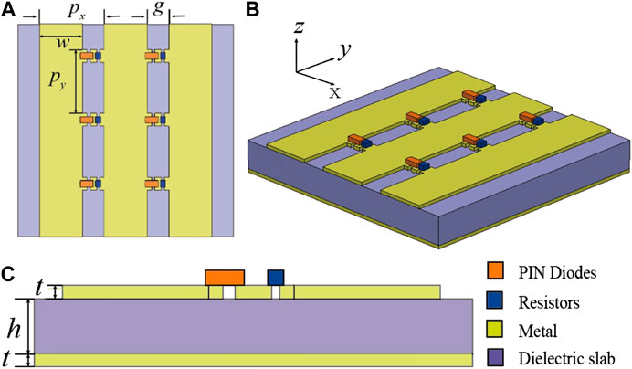
FIGURE 1. (A) Schematic diagram of the metasurface (top view). The purple part is dielectric, the yellow part is metal, the orange part represents diodes, and the blue part represents passive resistors. (B) 3D view of the metasurface. (C) side view of the metasurface.
According to the equivalent circuit model theory [23], a HIS can be modeled as a parallel RLC resonant circuit. The gap of grating behaves as a capacitor and the resonant loop forming among the top and the bottom layer provides an equivalent inductance, giving rise to a constant resonant frequency determined by the structural geometry. When the gap is loaded with a diode and a passive resistor, it turns into an active HIS with equivalent circuit model as shown in Figure 2. The diode forms a parallel RC circuit with the junction capacitance
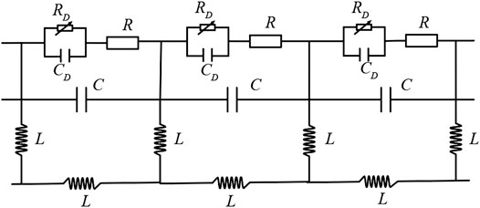
FIGURE 2. Equivalent circuit model of the active high impedance metasurface.
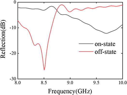
FIGURE 3. The simulated reflection spectra of the active high impedance metasurface when the loaded PIN diodes are on-state (black line) and off-state (red line).
For verification, a HIS sample is fabricated with printed circuit board (Taconic TLX-8) with a lateral size of 180 × 180 mm, as shown in Figure 4. 224 chip diodes and an equal number of chip resistors are surface mounted with gold silk bonding technology on the top layer of the sample. By alternatively applying positive and negative DC voltage on adjacent gratings, the diode is biased with tuneable voltage level.
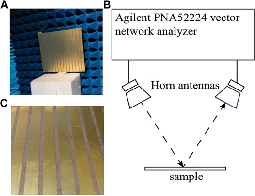
FIGURE 4. (A) The photo of experimental setup of the reflection measurement, (B) schematic experimental setup, and (C) the close-up photo of the sample.
The reflection is measured in a microwave anechoic chamber, with the sample placed on a foam and two standard gain horn antennas placed in front of it. The main lobe of horn antennas is perpendicularly incident on the sample surface, as schematically shown in Figure 4B. The horn emitter and the horn receiver are connected to an Agilent PNA52224 vector network analyzer to measure the S parameter S21. At first, a metal plate with the same size as the sample is measured to record the calibration field intensity. When the sample is under test, we get the reflected field intensity. Then the reflection coefficient is derived from the difference between these data.
We measured the reflection spectra for 0 V and +1.33 V bias voltage, corresponding to the off-state and on-state of diode respectively. Figure 5 shows the normalized reflection coefficient for both states from measurements. It can be observed that, when the bias is not loaded (0 V), the resonant absorption peak appears at 8.5 GHz with a reflection minimum of −24 dB. While applied with +1.33 V bias voltage, the absorption peak shifts to a higher frequency of 9.1 GHz, which agrees well with the theoretical calculation.
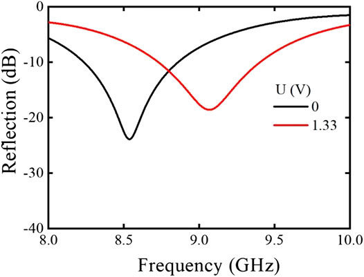
FIGURE 5. The measured reflection spectra of the active high impedance metasurface when the PIN diodes are loaded with +1.33 V bias voltage (red line) and in open-circuit state (black line).
In addition to the on-state and off-state, the resistance of the diode will continuously vary during the increase of positive bias voltage from 0 V to +1.33 V. The reflection of the sample is measured at several intermediate levels of bias voltage as shown in Figure 6. It is proved that the resonant absorption peak can be dynamically tuned between 8.5 and 9.1 GHz, by adjusting the bias voltage. The reflection of the sample is low than −18 dB during the whole range. When +1 V bias voltage is applied, the reflection coefficient drops below −30 dB, implying a wonderful absorption of incidence.
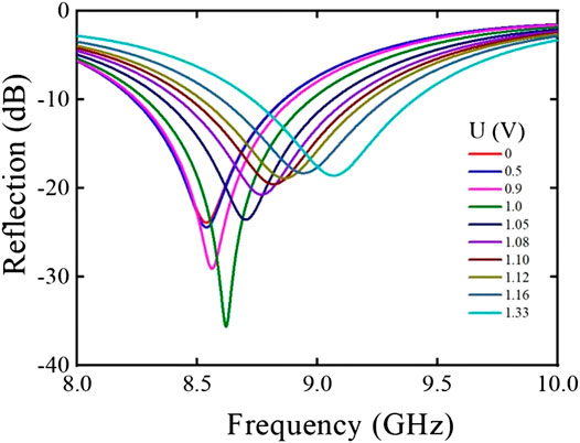
FIGURE 6. The measured reflection spectra when bias voltage varies from 0 to +1.33 V.
In conclusion, we have designed an active HIS to achieve dynamic control of the electromagnetic absorption. The impedance matching between the HIS and the incident wave is met by introducing a passive series resistor on the top surface of the HIS. By adjusting the positive bias voltage of the diode, the resistance of the diode can be tuned in a range to achieve dynamic control of the highly efficient electromagnetic absorption. Experimental samples are fabricated and measured to verify this phenomenon for the first time. Both theoretical simulations and experimental measurements demonstrate that the active HIS can achieve electromagnetic absorption with an absorption efficiency greater than 99% at resonant frequencies. By changing the diode from off-state to on-state, a dynamic switch between the electromagnetic absorption and reflection is observed at 8.5 and 9.1 GHz in experiments. Furthermore, continuous changing of the absorption peak between 8.5 and 9.1 GHz can be achieved by gradually varying the positive bias voltage of the diode. This work has great potential in electromagnetic wave stealth, shielding, and electromagnetic compatibility.
The original contributions presented in the study are included in the article/Supplementary Material, further inquiries can be directed to the corresponding authors.
ZW conceived the idea and supervised the whole study. HL and WX conducted the numerical calculations and performed the experiments. YC derived the theory, carried out the analysis and drafted the manuscript. All authors contributed to the review of manuscript.
This work is supported by the National Natural Science Foundation of China (Grant NOs 11674248, 11874285, 11204218, 62020106009, 61925504); supported by the Fundamental Research Funds for the Central Universities; Major Projects of Science and Technology Commission of Shanghai (Grant No. 17JC1400801); Pudong New Area Science and Technology Development Fund Industry-University-Research Special-Antenna Calibration and Test Equipment Research of 5G base Stations (Project No. PKX2019-D15).
Author YC was employed by the company Shanghai Mi Xuan Electronic Technology Co., Ltd.
The remaining authors declare that the research was conducted in the absence of any commercial or financial relationships that could be construed as a potential conflict of interest.
1. Yu N, Genevet P, Kats MA, Aieta F, Tetienne JP, Capasso F, et al. Light propagation with phase discontinuities: generalized laws of reflection and refraction. Science (2011) 334(6054):333–337. doi:10.1126/science.1210713
2. Yu N, Capasso F. Flat optics with designer metasurfaces. Nat Mater (2014) 13(2):139–150. doi:10.1038/nmat3839
3. Chen HT, Taylor AJ, Yu N. A review of metasurfaces: physics and applications. Rep Prog Phys (2016) 79(7):076401. doi:10.1088/0034-4885/79/7/076401
4. Glybovski SB, Tretyakov SA, Belov PA, Kivshar YS, Simovski CR. Metasurfaces: from microwaves to visible. Phy Rep (2016) 634:1–72. doi:10.1016/j.physrep.2016.04.004
5. Zhang L, Mei ST, Huang K, Qiu CW. Advances in full control of electromagnetic waves with metasurfaces. Adv Opt Mater (2016) 4(6):818–833. doi:10.1002/adom.201500690
6. Cheng KY, Wei ZY, Fan YC, Zhang XM, Wu C, Li HQ. Realizing broadband transparency via manipulating the hybrid coupling modes in metasurfaces for high-efficiency metalens. Adv Opt Mater (2019) 7(15):1900016. doi:10.1002/adom.201900016
7. Fan YC, Shen NH, Zhang FL, Zhao Q, Wei ZY, Zhang P, et al. Photoexcited graphene metasurfaces: significantly enhanced and tunable magnetic resonances. Acs Photonics (2018) 5(4):1612–1618. doi:10.1021/acsphotonics.8b00057
8. Wei Z, Cao Y, Su X, Gong Z, Long Y, Li H. Highly efficient beam steering with a transparent metasurface. Opt Express (2013) 21(9):10739–10745. doi:10.1364/OE.21.010739
9. Wei ZY, Cao Y, Fan YC, Yu X, Li HQ. Broadband polarization transformation via enhanced asymmetric transmission through arrays of twisted complementary split-ring resonators. Appl Phys Lett (2011) 99(22):221907. doi:10.1063/1.3664774
10. Bang S, Kim J, Yoon G, Tanaka T, Rho J. Recent advances in tunable and reconfigurable metamaterials. Micromachines (2018) 9(11):560. doi:10.3390/mi9110560
11. Fan K, Padilla WJ. Dynamic electromagnetic metamaterials. Mater Today (2015) 18(1):39–50. doi:10.1016/j.mattod.2014.07.010
12. Chowdhury DR, Singh R, O’Hara JF, Chen H-T, Taylor AJ, Azad AK. Dynamically reconfigurable terahertz metamaterial through photo-doped semiconductor. Appl Phys Lett (2011) 99:231101. doi:10.1063/1.3667197
13. Sun L, Zhang H, Dong G, Li P, Zhu Z, Li Y, et al. Dynamically tunable terahertz anomalous refraction and reflection based on graphene metasurfaces. Opt Commun (2019) 446:10–15. doi:10.1016/j.optcom.2019.04.058
14. Luo H, Cheng Y. Thermally tunable terahertz metasurface absorber based on all dielectric indium antimonide resonator structure. Opt Mater (2020) 102 doi:10.1016/j.optmat.2020.109801
15. Shadrivov IV, Morrison SK, Kivshar YS. Tunable split-ring resonators for nonlinear negative-index metamaterials. Opt Express (2006) 14(20):9344–9349. doi:10.1364/oe.14.009344
16. Xu HX, Tang S, Ma S, Luo W, Cai T, Sun S, et al. Tunable microwave metasurfaces for high-performance operations: dispersion compensation and dynamical switch. Sci Rep (2016) 6:38255. doi:10.1038/srep38255
17. Chen HT, Padilla WJ, Zide JM, Gossard AC, Taylor AJ, Averitt RD. Active terahertz metamaterial devices. Nature (2006) 444(7119):597–600. doi:10.1038/nature05343
18. Li Y, Lin J, Guo H, Sun W, Xiao S, Zhou L. A tunable metasurface with switchable functionalities: from perfect transparency to perfect absorption. Adv Opt Mater (2020) 8(6):1901548. doi:10.1002/adom.201901548
19. Sun Y, Tong Y-W, Xue C-H, Ding Y-Q, Li Y-H, Jiang H, et al. Electromagnetic diode based on nonlinear electromagnetically induced transparency in metamaterials. Appl Phys Lett (2013) 103(9):091904. doi:10.1063/1.4819854
20. Liu X, Padilla WJ. Dynamic manipulation of infrared radiation with MEMS metamaterials. Adv Opt Mater (2013) 1(8):559–562. doi:10.1002/adom.201300163
21. Arbabi E, Arbabi A, Kamali SM, Horie Y, Faraji-Dana M, Faraon A. MEMS-tunable dielectric metasurface lens. Nat Commun (2018) 9(1):812. doi:10.1038/s41467-018-03155-6
22. Sievenpiper D, Zhang L, Broas RF, Alexopolous NG, Yablonovitch E. High-impedance electromagnetic surfaces with a forbidden frequency band. IEEE Trans Microw Theor Tech (1999) 47(11):2059–2074. doi:10.1109/22.798001
23. Sievenpiper DF. High-impedance electromagnetic surfaces. IEEE Trans Microw Theor Tech (1999) 47(11):2059–2074. doi:10.1109/9780470545324.ch8
24. Zhou L, Wen W, Chan CT, Sheng P. Multiband subwavelength magnetic reflectors based on fractals. Appl Phys Lett (2003) 83(16):3257–3259. doi:10.1063/1.1622122
25. Hendevari MS, Bemani M, Nikmehr S. A novel dual-band double-sided high-impedance surface (DB-DS-HIS) with systematic design methodology. Int J Electron Commun (2020) 115:153039. doi:10.1016/j.aeue.2019.153039
26. Panda PK, Ghosh D. Wideband and high gain tuning fork shaped monopole antenna using high impedance surface. Int J Electron Commun (2019) 111:152920. doi:10.1016/j.aeue.2019.152920
27. Rao M, Sowmya N. Design and analysis of High impedance surface modified 3D antennas. CSI Transactions on ICT (2018) 6(2):173–177. doi:10.1007/s40012-018-0194-z
28. Wang L-L, Liu S-B, Zhang H-F, Kong X-K, Liu L-L. High-impedance surface-based flexible broadband absorber. J Electromagn Waves Appl (2017) 31(13):1216–1231. doi:10.1080/09205071.2017.1326850
29. Costa F, Monorchio A, Manara G. Analysis and design of ultra thin electromagnetic absorbers comprising resistively loaded high impedance surfaces. IEEE T Antenn Propag (2010) 58(5):1551–1558. doi:10.1109/tap.2010.2044329
30. Tretyakov SA, Maslovski SI. Thin absorbing structure for all incidence angles based on the use of a high-impedance surface. Microw Opt Technol Lett (2003) 38(3):175–178. doi:10.1002/mop.11006
Keywords: high-impedance, metasurface, dynamic control, eqivalent circuit model, magnetic resonance, absorption
Citation: Wei Z, Li H, Xu W and Cao Y (2021) Dynamic Control of Ultrathin Electromagnetic Absorber Using Active High Impedance Metasurfaces. Front. Phys. 8:632902. doi: 10.3389/fphy.2020.632902
Received: 24 November 2020; Accepted: 29 December 2020;
Published: 29 January 2021.
Edited by:
Qian Zhao, Tsinghua University, ChinaReviewed by:
Jiafu Wang, Air Force Engineering University, ChinaCopyright © 2021 Wei, Li, Xu and Cao. This is an open-access article distributed under the terms of the Creative Commons Attribution License (CC BY). The use, distribution or reproduction in other forums is permitted, provided the original author(s) and the copyright owner(s) are credited and that the original publication in this journal is cited, in accordance with accepted academic practice. No use, distribution or reproduction is permitted which does not comply with these terms.
*Correspondence: Zeyong Wei, d2VpemV5b25nQHRvbmdqaS5lZHUuY24=; Yang Cao, Y2FveWFuZzg1QDE2My5jb20=
Disclaimer: All claims expressed in this article are solely those of the authors and do not necessarily represent those of their affiliated organizations, or those of the publisher, the editors and the reviewers. Any product that may be evaluated in this article or claim that may be made by its manufacturer is not guaranteed or endorsed by the publisher.
Research integrity at Frontiers
Learn more about the work of our research integrity team to safeguard the quality of each article we publish.