- 1Key Laboratory of Specialty Fiber Optics and Optical Access Networks, Shanghai University, Shanghai, China
- 2State Key Laboratory of Millimeter Waves, Southeast University, Nanjing, China
A two-way Fano resonance switch in the plasmonic metamaterials has been proposed and experimentally demonstrated. The electrical Fano switch is composed of two concentric spoof localized surface plasmon (LSP) resonators. By adjusting the slit in the inner spoof LSP resonator, two different Fano resonance modes could be supported. By loading a Schottky barrier diode (SBD)across the slit in the inner LSP resonator, both Fano resonance modes can be simultaneously switched when the SBD is forward biased or reverse biased, and their switch status is opposite. Both simulated and measured results agree well at microwave frequencies and verify the two-way Fano resonance switch. The devices could be applied in many applications such as plasmonic circuits, multiway sensing or switching, and so on.
Introduction
In 1961, Ugo Fano discovered a new type of resonance in the study of the autoionizing states of atoms [1]. Unlike the symmetric lineshape of the Lorentzian resonance, the Fano resonance exhibits a distinctly asymmetric lineshape, which results from the destructive interference of a narrow discrete resonance with a broad continuum of states. The Fano interference is a universal phenomenon because the manifestation of configuration interference does not depend on the matter [2], which has been realized in many systems, such as photonic crystals [3], plasmonic nanostructures [4–9], metamaterials [10–13], plasmonic metamaterials [14–16], etc. Fano resonance may be used for the design of spin filters [17], switches [18], chemical or biological sensors [19–26], etc.
Active metamaterials are promising for the multifunctional systems with tunable, switchable, and non-linear functionalities [27]. For example, to conquer the bottleneck of Fano resonance sensing that the high Q factor Fano resonance is accompanied with an extremely small resonance intensity [28, 29], gain-assisted active spoof plasmonic Fano resonance is proposed to enhance both the Q factor and resonance intensity simultaneously [30]. Active Fano resonance switches were also demonstrated. The on–off switching of the Fano resonance of a plasmonic cluster by its incorporation into a polarization rotating liquid crystal device was demonstrated in a voltage-dependent manner [31]. Electrically controlled damping of Fano resonance in a graphene-nanoantenna hybrid device was observed [32]. Active photoswitching of sharp Fano resonances in silicon-implanted terahertz asymmetric metallic split-ring resonator structure was demonstrated, where the strength of the Fano resonance is modulated by changing the optical pump powers [33]. By changing the pH value of the solution environment, the active plasmonic Fano resonance switching is enabled by varying the refractive index of a layer of polyaniline between the Au nanosphere and the Au nanoplate [34]. The Fano resonance generated in Si nanosphere dimers on a VO2 layer can be actively tuned by utilizing the phase transition of VO2 with temperature [35]. However, there are still great challenges that are difficult to overcome, such as slow switching speed, high operation voltage, low contrast of modulation, etc. Furthermore, it is impossible to achieve two-way or multiway Fano switches based on the discussed mechanisms.
Here, we investigated an electrically two-way Fano resonance switch in the plasmonic metamaterials, which is composed of two concentric spoof localized surface plasmon (LSP) resonators. It has been demonstrated that there would be two different Fano resonance modes when adjusting the slit in the inner spoof LSP resonator. By loading a Schottky barrier diode (SBD) across the slit in the inner LSP resonator, both Fano resonance modes can be simultaneously controlled (OFF/ON) when the SBD diode is forward biased or reverse biased. Hence, a two-way Fano resonance switch can be realized. Both simulated and measured results agree well at microwave frequencies.
Passive Spoof Plasmonic Fano Resonance
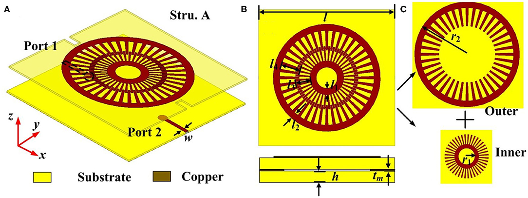
To understand the physical mechanism of the two-way Fano resonance switch, we first investigate the Fano resonances of two spoof plasmonic Fano resonance Structures A and B. The three-dimensional (3D) schematic of Structure A is illustrated in Figure 1A, which contains two vertically stacked layers. The top layer is the spoof plasmonic Fano resonator, and the bottom layer is a microstrip feeding line. The top view and side view of Structure A are shown in Figure 1B, where the length l of the spoof plasmonic Fano resonator is 52 mm. The width w of the microstrip line is 1.3 mm, and the thickness h of the substrate and the thickness tm of the copper are 0.5 and 0.018 mm, respectively. As demonstrated in Figure 1C, the spoof plasmonic Fano resonator is composed of two concentric spoof LSP resonators. The outer and inner corrugated metallic rings are printed on the dielectric substrate (F4B), whose relative dielectric permittivity is 2.65, and loss tangent is 0.002. The radiuses r1 and r2 of the inner and outer corrugated rings are 1.5 and 10.5 mm, respectively. Both the lengths l1 and l2 are 2.5 mm, and the groove depths l3 and l4 are 5 and 7.5 mm, respectively.

Figure 1. Spoof plasmonic Fano resonance Structure A. (A) Three-dimensional schematic of Structure A, (B) top view and side view of Structure A, and (C) outer and inner corrugated rings.
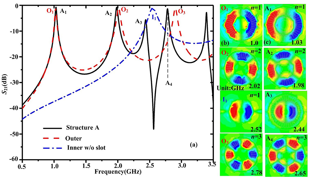
The transmission coefficients (S21) are plotted in Figure 2a, which are obtained by using the commercial software HFSS. The driven modal solver is used. The wave port and the radiation boundary condition are adopted. The minimum mesh size is 0.06 mm. The spoof LSP modes with Lorentzian lineshapes of outer and inner corrugated rings are marked as O1, O2, O3, and I1 modes. The corresponding resonant frequencies are 1.0, 2.02, 2.78, and 2.52 GHz, respectively. Figure 2b illustrates the 2D Ez-field distributions on the xoy plane 2 mm above the spoof LSP resonators, where it can be seen that the spoof LSP modes O1-O3 are dipolar mode (n = 1), quadrupolar mode (n = 2), and hexapolar mode (n = 3) for the outer corrugate ring. The spoof LSP mode I1 is the dipolar mode (n = 1). For structure A, the resonant peaks are denoted by A1, A2, A3, and A4. The corresponding resonant frequencies are 1.03, 1.98, 2.44, and 2.65 GHz, respectively. It can be seen that there exists an asymmetric Fano lineshape between A2 and A4, which stems from the destructive interference of the narrow discrete spoof LSP mode I1 with the broad continuum state between modes O2 and O3 of the outer corrugated ring. Figure 2c illustrates the 2D Ez-field distributions on the xoy plane 2 mm above Structure A. It can be clearly observed that the modes A1, A2, and A4 are corresponding to the spoof LSPs modes O1, O2, and O3, respectively, while the resonant peak A3 corresponds to the spoof LSPs mode I1.

Figure 2. (a) Simulation transmission coefficients S21 of Structure A, outer corrugated ring, and inner corrugated ring. Two-dimensional Ez-field distributions on the xoy plane 2 mm above (b) the spoof localized surface plasmon (LSP) resonators and (c) Structure A.
Next is structure B, whose 3D schematic is illustrated in Figure 3A. The top view of Structure B is shown in Figure 3B. From Figure 3C, it can be seen that Structure B is also composed of two concentric LSP resonators. The difference with Structure A is that there is a slit in the inner corrugated ring, where the slit is cut at the position of θ = 90°.

Figure 3. Spoof plasmonic Fano resonance Structure B. (A) Three-dimensional schematic of Structure B, (B) top view of Structure B, and (C) outer corrugated ring and the inner corrugated ring with a slit.
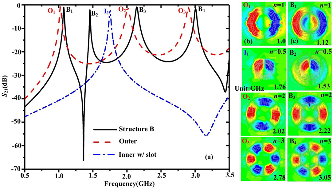
The simulation transmission coefficients S21 of Structure B, outer corrugated ring, and inner corrugated ring with a slit are given in Figure 4a. The LSP modes are different for the inner corrugated ring and the corrugated ring with a slit. Here, the spoof LSP modes of outer and inner corrugated rings are also marked as O1, O2, O3, and I1 modes. Figure 4b illustrates the corresponding 2D Ez-field distributions on the xoy plane 2 mm above the spoof LSP resonators. The resonant frequencies of the outer corrugated ring are the same, and the spoof LSP modes Ez-field distributions are also unchanged, as shown in Figure 4b. It can be seen that the resonant frequency of the inner ring with a slit has changed from 2.52 to 1.76 GHz, as the mode I1 of the inner ring with a slit is the half-integer LSP mode (n = 0.5). For structure B, the resonant peaks are marked as B1, B2, B3, and B4. The corresponding resonant frequencies are 1.12, 1.53, 2.22, and 3.05 GHz, respectively. We can see that there appears an asymmetric Fano lineshape between B1 and B3, which results from the destructive interference of the narrow discrete mode I1 with the broad continuum state between modes O1 and O2 of the outer corrugated ring, and there is no resonance mode between modes O2 and O3 of the outer corrugated ring. Figure 4c illustrates the 2D Ez-field distributions on the xoy plane 2 mm above Structure B. It can be clearly observed that the modes B1, B3, and B4 are corresponding to the spoof LSPs modes O1, O2, and O3, respectively, whereas the resonant peak B2 corresponds to the mode I1.

Figure 4. (a) Simulation transmission coefficients S21 of Structure B, outer corrugated ring, and inner corrugated ring with a slit. Two-dimensional Ez-field distributions on the xoy plane 2 mm above (b) the spoof LSPs resonators and (c) Structure B.
Active Two-Way Fano Resonance Switch
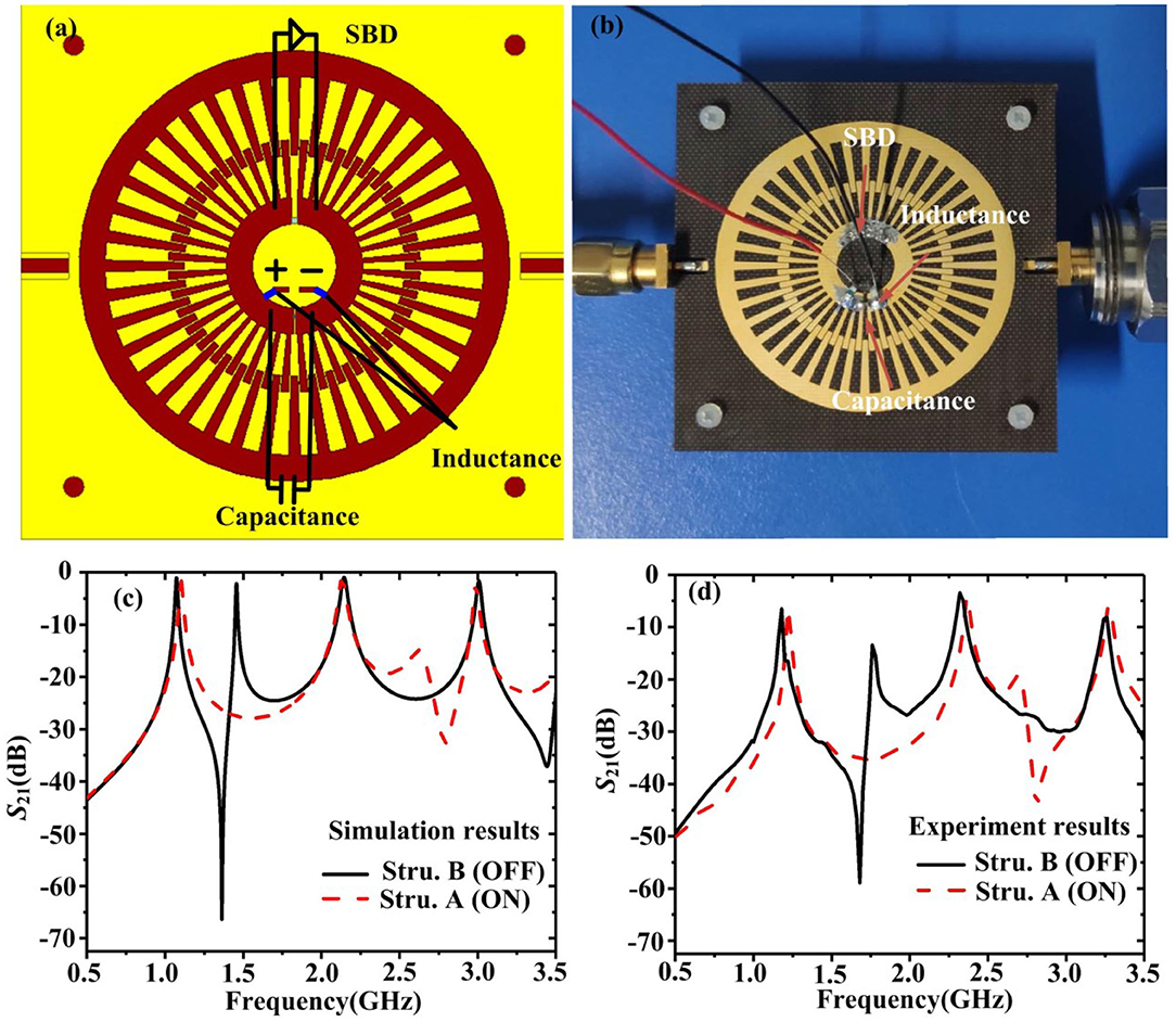
Considering the responses of passive Structure A and Structure B, it can be concluded that when there exists a slit in the inner corrugated ring, the Fano resonance appears between the O1 and O2 modes, and when there is no slit in the inner corrugated ring, the Fano resonance appears between the O2 and O3 modes. Hence, if a switch diode is loaded across the slit, the two Fano resonance modes could be switched. As there is no charge carrier depletion region at the junction, the SBD diode has a shorter recovery time than the PIN diode. For a small signal, the switching time of the SBD diode is only 100 ps. Here, an SBD diode (MACOM MA4E 1317) is used to switch the Fano resonance mode, whose operating bias voltage is 0.6–0.8 V. The optimum bias voltage is 0.75 V. The DC voltage source is GW Instek linear DC power supplies GPS-1850D. Figure 5a illustrates the schematic of the active two-way Fano resonance switch, where an SBD diode is mounted across the slit in the inner corrugated ring. The capacitance is used to isolate the DC signal, whereas the inductance is used to isolate the AC signal. The fabricated sample is shown in Figure 5b. In the simulation, the SBD is equivalent to an RLC series circuit, where Rs is the series resistance, Ls is the inductance arising from the metallic contacting strap, and Cj is the diode junction capacitance, and the values are 4 Ω, 0.45 nH, and 0.02 pF, respectively. The simulated transmission coefficients S21 are plotted in Figure 5c. It can be seen that when the SBD diode is forward biased (ON), there is no slit in the corrugated ring. The structure is equivalent to Structure A, where the second Fano resonance appears. When the SBD diode is reverse biased (OFF), there is a slit in the corrugated ring. The structure is equivalent to Structure B, where the first Fano resonance appears. Hence, a two-way Fano resonance switch could be realized. The sample is measured by using a vector network analyzer (Agilent N5227A). The experimental results shown in Figure 5d agree well with the simulation results. When the diode is ON, the Fano resonance appears between the quadrupolar mode and hexapolar mode. When the diode is OFF, the Fano resonance appears between the dipolar mode and the quadrupolar mode. The measured transmission coefficients are almost 10 dB lower than the simulation results, which may be caused by the higher series resistance Rs and the welding quality in the measurements.

Figure 5. (a) Schematic of the active two-way Fano resonance switch. (b) Fabricated sample. (c) Simulated and (d) measured transmission coefficients S21 of the active two-way Fano resonance switch.
Conclusion
In summary, we have proposed and experimentally demonstrated an active two-way Fano resonance switch in the microwave frequency. When the SBD diode is forward biased, the second Fano resonance appears between the quadrupole mode and hexapole mode. When the SBD diode is reverse biased, the first Fano resonance appears between the dipolar mode and the quadrupole mode. The experimental results agree well with the simulated results. The Fano resonance switch has advantages such as two-way switches, fast switching speed, and low operation voltage, which could find applications in plasmonic circuits, sensors, devices, etc.
Data Availability Statement
All datasets presented in this study are included in the article/supplementary material.
Author Contributions
All authors listed have made a substantial, direct and intellectual contribution to the work, and approved it for publication.
Funding
This work was supported in part by the National Natural Science Foundation of China under grant no. 61971469, in part by the Science and Technology Commission of Shanghai Municipality (STCSM) under grant no. 18ZR1413500, and in part by the Open Project Program of the State Key Laboratory of Millimeter Waves under grant no. K202109.
Conflict of Interest
The authors declare that the research was conducted in the absence of any commercial or financial relationships that could be construed as a potential conflict of interest.
References
1. Fano U. Effects of Configuration Interaction on Intensities and Phase Shifts. Phys Rev. (1961) 124:1866–78. doi: 10.1103/PhysRev.124.1866
2. Yong S .J, Arkady MS, Chang SK. Classical analogy of Fano resonances. Phys Scr. (2006) 74:259–66. doi: 10.1088/0031-8949/74/2/020
3. Rybin MV, Khanikaev AB, Inoue M, Samusev KB, Steel MJ, Yushin G, et al. Fano resonance between Mie and Bragg scattering in photonic crystals. Phys Rev Lett. (2009) 103:023901. doi: 10.1103/PhysRevLett.103.023901
4. Bachelier G, Russier AI, Benichou E. Fano profiles induced by near-field coupling in heterogeneous dimers of gold and silver nanoparticles. Phys Rev Lett. (2008) 101:197401. doi: 10.1103/PhysRevLett.101.197401
5. Liu N, Langguth L, Weiss T. Plasmonic analogue of electromagnetically induced transparency at the Drude damping limit. Nat Mater. (2009) 8:758–762. doi: 10.1038/nmat2495
6. Verellen N, Sonnefraud Y, Sobhani H. Fano resonances in individual coherent plasmonic nanocavities. Nano Lett. (2009) 9:1663–7. doi: 10.1021/nl9001876
7. Sonnefraud Y, Verellen V, Sobhani H, Guy AE, Victor VM. Experimental realization of subradiant, superradiant, and Fano resonances in ring/disk plasmonic nanocavities. ACS Nano. (2010) 4:1664–70. doi: 10.1021/nn901580r
8. Miroshnichenko AE, Flach S, Kivshar YS. Fano resonances in nanoscale structures. Rev Mod Phys. (2010) 82: 2258–90. doi: 10.1103/RevModPhys.82.2257
9. Fu YH, Zhang JB, Yu YF. Generating and manipulating higher order fano resonances in dual-disk ring plasmonic nanostructures. ACS Nano. (2012) 6:5130–7. doi: 10.1021/nn3007898
10. Fedotov VA, Rose M, Prosvirnin SL, Papasimakis N, Zheludev NI. Sharp trapped-mode resonances in planar metamaterials with a broken structural symmetry. Phys Rev Lett. (2007) 99:147401. doi: 10.1103/PhysRevLett.99.147401
11. Zhang S, Genov DA, Wang Y, Liu M, Zhang X. Plasmon-induced transparency in metamaterials. Phys Rev Lett. (2008) 101:047401. doi: 10.1103/PhysRevLett.101.047401
12. Boris L, Nikolay IZ, Stefan AM, Naomi JH, Peter N, Harald G, et al. The fano resonance in plasmonic nanostructures and metamaterials. Nat Mater. (2010) 9:707–15. doi: 10.1038/nmat2810
13. Singh R, Al-Naib IAI, Koch M, Zhang W. Sharp fano resonances in THz metamaterials. Opt Express. (2011) 19:6312–9. doi: 10.1364/OE.19.006312
14. Liao Z, Pan BC, Shen XP, Cui TJ. Multiple fano resonances in spoof localized surface plasmons. Opt Express. (2014) 22:15710. doi: 10.1364/OE.22.015710
15. Xiao QX, Yang BJ, Zhou YJ. Spoof localized surface plasmons and Fano resonances excited by flared slot line. J Appl Phys. (2015) 118:233112. doi: 10.1063/1.4938153
16. Chen L, Xu NN, Singh L, Cui TJ, Singh R, Zhu YM, et al. Defect-induced fano resonances in corrugated plasmonic metamaterials. Adv Opt Mat. (2017) 5:1–7. doi: 10.1002/adom.201600960
17. Song JF, Ochiai Y, Bird JP. Fano resonances in open quantum dots and their application as spin filters Appl Phys Lett. (2003) 82:4561. doi: 10.1063/1.1586788
18. Sámson ZL, MacDonald KF, De Angeils F. Metamaterial electro-optic switch of nanoscale thickness. Appl Phys Lett. (2010) 96:143105. doi: 10.1063/1.3355544
19. Chung YC, Jay Guo L. Biochemical sensors based on polymer microrings with sharp asymmetrical resonance. Appl Phys Lett. (2003) 83:1–4. doi: 10.1063/1.1605261
20. Lahiri B, Khokhar AZ, De La Rue RM, McMeekin SG, Johnson NP. Asymmetric split ring resonators for optical sensing of organic materials. Opt Express. (2009) 17:1107–15. doi: 10.1364/OE.17.001107
21. Liu N, Weiss T, Mesch M. Planar metamaterial analogue of electromagnetically induced transparency for plasmonic sensing. Nano Lett. (2010) 10:1103–7. doi: 10.1021/nl902621d
22. Hua L, Xueming L, Dong M, Guoxi W. Plasmonic nanosensor based on fano resonance in waveguide-coupled resonators. Opt Lett. (2012) 37:3780. doi: 10.1364/OL.37.003780
23. Ranjan S, Wei C, Ibraheem A, Longqing C, Withawat W, Weili Z. Ultrasensitive terahertz sensing with high-Q fano resonances in metasurfaces. Appl Phys Lett. (2014) 105:1–6. doi: 10.1063/1.4895595
24. Elena S, Ran D, George S, Ravindra P. Sensing based on fano-type resonance response of all-dielectric metamaterials. Sensors. (2015) 15:9344–59. doi: 10.3390/s150409344
25. Kuang LL, Hsuan YH, Meng LY, Chia CC, Ming YP, Xu S, et al. Highly sensitive aluminum based biosensors using tailorable fano resonances in capped nanostructures. Sci Rep. (2017) 7:44104. doi: 10.1038/srep44104
26. Chen J, Gan F, Wang Y. Plasmonic sensing and modulation based on fano resonances. Adv Opt Mater. (2018) 6:1701152. doi: 10.1002/adom.201701152
27. Zheludev NI, Kivshar YS. From metamaterials to metadevices. Nat Mater. (2012) 11:917–24. doi: 10.1038/nmat3431
28. Cong LQ, Manjappa M, Xu NN, Al NI, Zhang WL, Singh R. Fano resonances in terahertz metasurfaces: a figure of merit optimization. Adv Opt Mater. (2015) 3:1537. doi: 10.1002/adom.201500207
29. Bochkova E, Han S, Lustrac A, Singh R, Burokur SN, Lupu A. High-Q fano resonances via direct excitation of an antisymmetric dark mode. Opt Lett. (2018) 43:3818. doi: 10.1364/OL.43.003818
30. Zhou YJ, Li QY, Zhao HZ, Cui TJ. Gain-assisted active spoof plasmonic fano resonance for high-resolution sensing of glucose aqueous solutions. Adv Mater Technol. (2019) 5:1900767. doi: 10.1002/admt.201900767
31. Chang WS, Lassiter JB, Swanglap P, Sobhani H, Khatua S, Nordlander P, et al. A plasmonic fano switch. Nano Lett. (2012) 12:4977–82. doi: 10.1021/nl302610v
32. Emani NK, Chung TF, Kildishev AV, Shalaev VM, Chen YP, Boltasseva A. Electrical modulation of fano resonance in plasmonic nanostructures using graphene. Nano Lett. (2014) 14:78–82. doi: 10.1021/nl403253c
33. Manukumara M, Yogesh KS, Longqing C, Ibraheem AN, Ranjan S. Active photo switching of sharp fano resonances in THz metadevices. Adv Mater. (2017) 29:1603355. doi: 10.1002/adma.201603355
34. Lu W, Cui X, Chow TH, Shao L, Wang H, Chen H, et al. Switching plasmonic fano resonance in gold nanosphere-nanoplate heterodimers. Nanoscale. (2019) 11:9641–53. doi: 10.1039/C9NR01653H
Keywords: Fano resonance, localized surface plasmons (LSPs), plasmonic, metamaterials (MMs), switchable
Citation: Zhou YJ, Dai LH, Li QY and Xiao ZY (2020) Two-Way Fano Resonance Switch in Plasmonic Metamaterials. Front. Phys. 8:576419. doi: 10.3389/fphy.2020.576419
Received: 26 June 2020; Accepted: 22 September 2020;
Published: 22 October 2020.
Edited by:
Lin Chen, University of Shanghai for Science and Technology, ChinaReviewed by:
Dejun Liu, Shanghai Normal University, ChinaBai Cao Pan, Hangzhou Dianzi University, China
Copyright © 2020 Zhou, Dai, Li and Xiao. This is an open-access article distributed under the terms of the Creative Commons Attribution License (CC BY). The use, distribution or reproduction in other forums is permitted, provided the original author(s) and the copyright owner(s) are credited and that the original publication in this journal is cited, in accordance with accepted academic practice. No use, distribution or reproduction is permitted which does not comply with these terms.
*Correspondence: Yong Jin Zhou, eWp6aG91QHNodS5lZHUuY24=
 Yong Jin Zhou
 Li Hui Dai1