
94% of researchers rate our articles as excellent or good
Learn more about the work of our research integrity team to safeguard the quality of each article we publish.
Find out more
ORIGINAL RESEARCH article
Front. Phys. , 29 September 2020
Sec. Optics and Photonics
Volume 8 - 2020 | https://doi.org/10.3389/fphy.2020.00385
This article is part of the Research Topic Advanced Photonics Metasurfaces: Design, Fabrication, and Applications View all 15 articles
In this article, we propose the design of a multispectral metasurface (MSM), which can simultaneously achieve quite good optical transparency, low infrared (IR) emissivity, and wideband microwave absorption. To this end, optically transparent materials were used in the MSM design, including indium tin oxide, polyethylene terephthalate, and polymethyl methacrylate. The MSM is composed of three functional layers: a frequency-selective surface (FSS) on the top, a resistively absorbing layer in the middle and a complete conducting sheet at the bottom. Because of large occupation ratio of conducting area and the low-pass property of the FSS, electromagnetic waves are allowed to penetrate through it into the middle absorbing layer, simultaneously with low surface IR emissivity. A prototype was designed, fabricated, and measured. Both the simulation and experiment results show that the MSM can achieve strong absorption of > 90% in 12.03–29.43 GHz and low IR emissivity of about 0.3 in 3.0–14.0 μm simultaneously. Moreover, the average optical transparency is higher than 90%. Because of the excellent multispectral compatibility, the MSM may find applications in electromagnetic protection, stealth technologies, etc.
Metamaterials as artificial materials could actualize the propagation characteristic of manipulating electromagnetic wave [1, 2]. Plenty of metamaterial structures are designed as low-scattering materials, perfect absorbers, invisible cloak, surface wave suppressing materials, and so on [3–10]. With the rapid development of the technologies of metamaterials, the function of single-waveband materials can no longer satisfy the needs of various applications. It is the mainstream to design the multispectral metasurfaces (MSMs) to apply under a variety of environments [11–16]. According to spectroscopy, microwave band, infrared (IR) band, and visible light band are the most commonly used region. However, the mechanisms of microwave and IR counter each other in stealth technology. The mechanism of radar for microwave is to reduce echoes from the detected objects [17–20]. In contrast, IR detection requires the low-emissivity materials to be undetected. According to Kirchhoff's law, high-reflectivity materials, which are low emitters, should be needed for IR band. Therefore, this problem needs to be solved in our design thought.
Many scientists have studied the metasurfaces in multiband applications. Wang et al. [21] designed IR-radar bistealth frequency-selective surface (FSS) with IR emissivity below 0.3 and above 90% absorption in 8–18 GHz for microwave band. Zhong et al. [22] proposed a thin artificial structure with wideband absorption from 3 to 8 GHz up to incident angles of 30° and low IR emission value of 0.2. Hao et al. [23] designed a stealth-compatible structure consisting of metallic FSS and resistive FSS with reflectivity below –10 dB in whole radar X wave band and IR emissivity < 0.3 in the IR region of 8–14 μm. Pang et al. [24] fabricated an HMS with an efficient reflection reduction larger than 10 dB in the frequency band of 8.2–18 GHz and low IR emissivity < 0.27 from 3 to 14 μm. Zhang et al. [25] present a thin metasurface with broadband microwave absorptivity > 8.2–16.0 GHz and low IR emissivity in the region from 8 to 14 μm.
Except for using metals, scientists also chose the visible transparent materials for studying these problems to use in more scenes, such as using indium tin oxide as main materials, polymethyl methacrylate (PMMA) as dielectric material, and so on. Xu et al. [26] proposed optically transparent metamaterial structure with a high absorptivity > 90% in the region of 6.28–12.29 GHz for TE polarization, and the absorptivity in the region of 7.19–15.26 GHz is > 90% for TM polarization. Its IR emissivity is about 0.30 in the IR region from 3 to 14 μm. Shuomin et al. [27] deposited four indium tin oxide films on metasurface in order to realize a low microwave reflectivity < 0.1 from 1.5 to 9 GHz and a thermal emissivity approaching 0.52.
In microwave band, radar absorbers must be the most stable application. As the absorber, the operational bandwidth is the most important parameter. In this article, we propose the design of an MSM that can simultaneously achieve quite good optical transparency, low IR emissivity, and wideband microwave absorption. To this end, optically transparent materials were used in the metasurface design, including indium tin oxide, polyethylene terephthalate (PET), and PMMA. The MSM is composed of three functional layers: an FSS on the top, a resistively absorbing layer in the middle, and a complete conducting sheet at the bottom. Because of large occupation ratio (OR) of conducting area and the low-pass property of the FSS, electromagnetic waves are allowed to penetrate through it into the middle absorbing layer, simultaneously with low surface IR emissivity. A prototype was designed, fabricated, and measured. Both the simulation and experiment results show that the MSM can achieve strong absorption > 90% in 12.03–29.43 GHz and low IR emissivity about 0.3 in 3.0–14.0 μm simultaneously. Moreover, the average optical transparency is higher than 90%. To better observe our properties of our MSM, the compared results of typical compatible metamaterials are presented as Table 1. It can be observed clearly that our MSM has the best properties.
In IR band, the most commonly used materials are metals because of their low emissivity property, such as gold, aluminum, silver, copper, etc. However, when human needs the perspective property of the naked eyes, these metals could not work anymore. Thus, in this article, a fabricated MSM chose the ITO as the main material and utilized PET and PMMA as dielectric material to achieve the feature of the visible transparency. And the ITO also has the property of metal, so it is appropriate that metals are replaced by ITO.
In the design process of the MSM, the tailored structure was divided into three functional layers: an FSS on the top, a resistively absorbing layer in the middle, and a complete conducting sheet at the bottom, as depicted in Figure 1. The electromagnetic waves, including IR wave, microwave, and visible, propagate in different directions after working with the MSM. Because of the existence of the top layer, which consists of the ITO patches as the low emissivity of IR layer (LIRL), it has the property of displaying low temperature. For the microwave, it must pass through the low-emissivity top layer and work at the resistively absorbing layer. Thus, it must be a loss-pass and high-resistance FSS to make the radar wave propagate to the resistively absorbing layer as the wideband microwave absorber (WMA) and be absorbed. For visible light, because of the optical transparent materials, it can achieve visible transparence.
Figure 2 depicts the unit of the MSM structure. Figures 2A,B exhibit LIRL and WMA, respectively. And the resistance of LIRL and WMA is different. The LIRL's resistance is 6 Ω/Sq, and that of WMA is 30 Ω/Sq. The side view is shown in Figure 2C. And the thicknesses of two stealth layers' PET are different. The thickness of LIRL's is 0.175 mm, and that of WMA's is 0.125 mm. The other parameters are D = 1 mm, d = 0.1 mm, L = 19 mm, l1 = 18.7 mm, l2 = 11.8 mm, Φ1 = 4.8 mm, Φ2 = 3 mm, D1 = 0.5 mm, D2 = 1 mm, and the ITO of LIRL OR is 81%.
Because the emissivity of ITO is low, in the IR band, the total IR emissivity ε can be calculated by the square rate in the following formula:
where ε in Equation (1) is the emissivity of the MSM, and the εi and εp are emissivities of the ITO and PET, respectively. And the fi is the OR of the ITO's area to that of the metasurface. The fp is the OR of the PET's to metasurface's. For this MSM, the emissivity of the PET is high, nearly > 0.8, but filling ratio is < 0.2, so the emissivity of the MSM lower than 0.3.
In the microwave band, the simulation results were obtained by the commercial software CST Microwave Studio. The unit cell condition is set in the x–y direction, and in the z direction, the open boundary condition is chosen. The absorption can be calculated by Equation (2),
where |S21|2 and |S11|2, respectively, represent the transmissivity and reflectivity. However, the microwave could not propagate through the MSM because of the bottom a complete conducting sheet of ITO without gaps, so the average transmission is nearly zero. For this reason, Equation (2) could be simplified as Equation (3).
MSM could be equivalent to the circuit as shown in Figure 3. Z0 is the impendence of free space, which is equal to 377 Ω. ZL and ZW are the equivalent impendence of the LIRL and WMA, respectively.
We can calculate the ABCD matrix as Equation (4), where θ = βt, β = 2π/λ:
The calculated absorption curves including TE and TM polarization are exhibited in Figure 4A. The MSM showed a strong absorptivity of > 90% from 12.03 to 29.43 GHz. And the simulation results of different polarizing angles ϕ are depicted in Figure 4B to indicate that the tailored structure is polarization independent significantly. The calculated absorption curves at different incident angles are shown in Figure 4C. And it reveals that the absorption of the MSM is > 80% within 40° of incident angles.

Figure 4. (A) Simulated absorption at different polarization modes for TE polarized and TM polarized. (B) Simulated absorption at different polarization modes for full angle domain. (C) Simulated absorption at different incident angles.
In order to uncover the physics mechanism of the microwave absorption, the surface current distributions and electric field at resonant frequencies were chosen.
On the idea of designing the LIRL, the microwave must propagate through it and work at the WMA. According to the above reasons, a loss-pass and high-resist FSS is chosen, as shown in Figure 5. To explain the physics mechanism of the microwave absorption behavior, based on the result of simulation, three resonant frequencies are chosen, f = 13.33, 24.43, and 27.85 GHz, with absorbance of 96.54, 97.65, and 95.68%, respectively.
It could be observed that an electric current loop is formed between the top and bottom layer as Figures 6–8 depicted. It means that a magnetic dipole is at work to obtain the absorption peak of microwave.
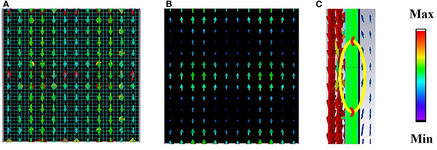
Figure 6. Distribution of surface current resonance frequency f = 13.33 GHz: (A) top view, (B) bottom view, (C) side view.
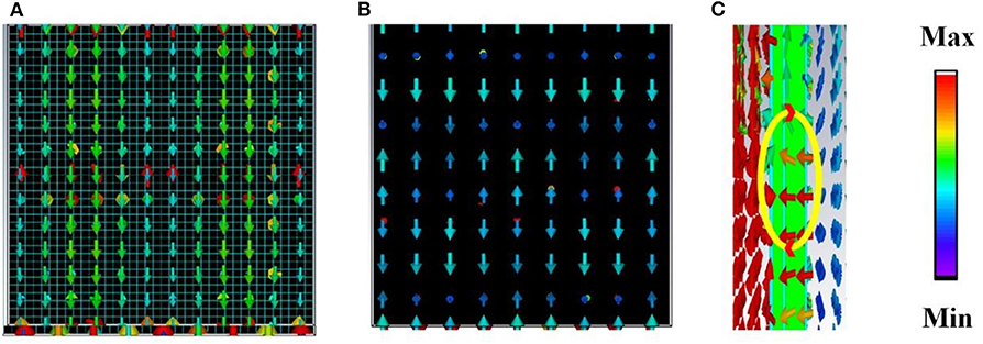
Figure 7. Distribution of surface current resonance frequency f = 24.43 GHz: (A) top view, (B) bottom view, (C) side view.
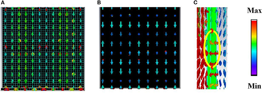
Figure 8. Distribution of surface current resonance frequency f = 27.85 GHz: (A) top view, (B) bottom view, (C) side view.
To understand the resonant modes of the three resonance frequencies at the WMA, the distribution of the electric field is shown in Figure 9. It is clear to observe that their strong interaction with the position of ITO ring is different. Figure 9A depicts that the resonant mode at f = 13.33 GHz is mostly the circular ring. By contrast, at f = 27.85 GHz, the resonant mode is mostly ITO square ring as Figure 9B shows. And as presented in Figure 9C, the mode at f = 34.43 GHz includes the circular ring and the square ring.
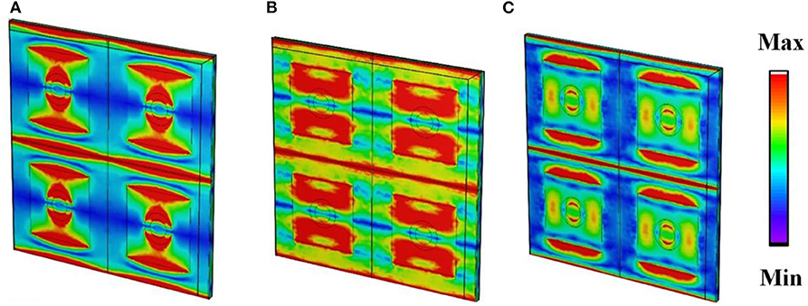
Figure 9. Distribution of the electric field of WMA (A) f = 13.33 GHz, (B) f = 24.43 GHz, (C) f = 27.85 GHz.
A 300 × 300-mm sample was tailored by the printed circuit board technique to check the simulation result of the MSM. The PBC technique is one of the electron printing techniques. In our article, we adopted this printing technique to obtain a more accurate sample. First, ITO was deposited on the whole PET board. After depositing, the PBC technique was adopted, which uses laser to etch on the ITO film to tailor the shape of the structure we need. In the article, the shape we need is the ITO patches in LIRL, the circular ring and square ring in WMA, as shown in Figure 10.
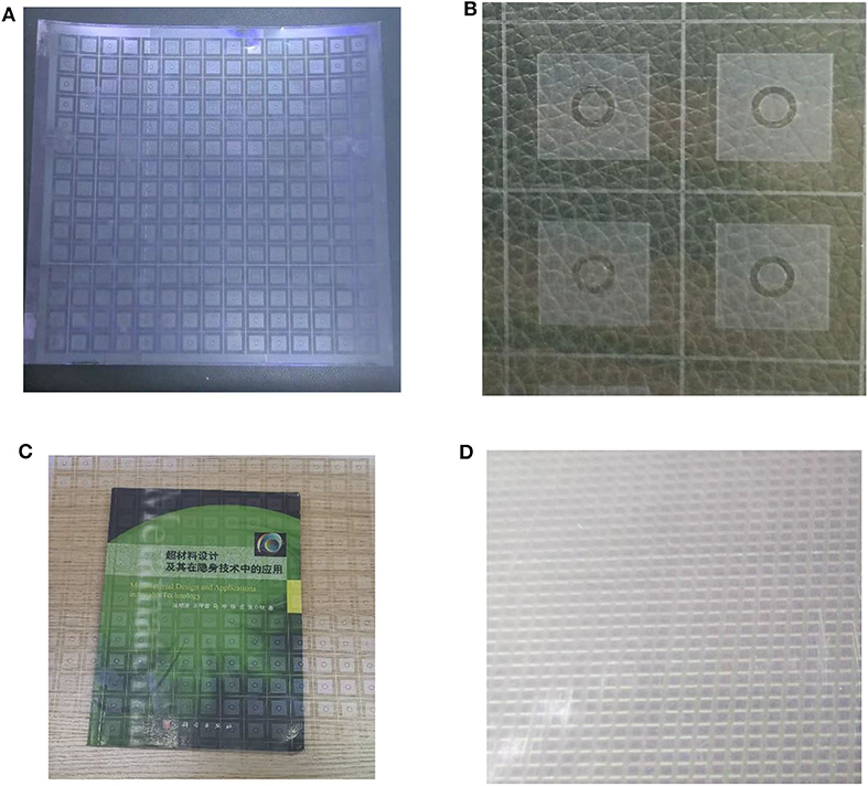
Figure 10. (A) the photograph of WMA, (B) a large version of WMA, (C) visible transparent property of WMA, (D) a large version of LIRL.
For microwave-absorbing ability, an Agilent 8720ET vector network analyzer was used to measure the reflection of microwave. The detection scene is presented as shown in Figure 11.
The microwave was perpendicular to the sample, and the distance between structure and antennas was 500 mm. The test result is depicted in Figure 12. The tendency of the measured result and simulated result is consistent. However, the test result is better than the simulation possibly because of the thinner processed thickness of the dielectric layer.
For IR low emissivity property, TSS-5X IR emissivity and G100EX thermal camera were utilized for test. In order to get a direct analysis result, a PET board with the same size was compared with the sample. The IR emittance results were presented in Figure 13. Its back and the PET board were 0.27, 0.19, and 0.91, respectively, matching the intended results.
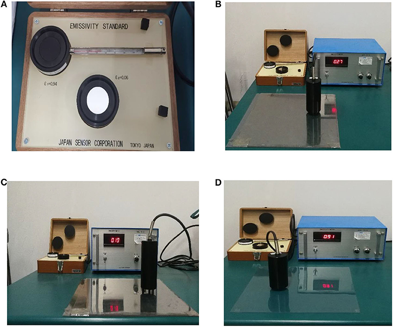
Figure 13. (A) the emissivity standard of IR emissivity, (B) the measurement result of the sample, (C) the measurement result of the sample's back, (D) the measurement result of the reference.
A qualitative experiment was conducted to better testify the IR-stealth property of the sample. The sample and the same size PET board were heated at the same temperature by HZ-2019A high–low temperature test chamber. And then the G100EX thermal camera was used to compare their IR thermal images.
It is direct to reveal that the IR-stealth capacity of MSM is effective as shown in Figure 14. Heated at the same 45° temperature, their IR thermal images show great differences. At 24.9° environment temperature (c point), the temperature of PET was 43.8° (a point), whereas the sample only showed 26.6° (b point), as displayed in Figure 14B.
The visible transmittances spectra of the sample are tested by ultraviolet-visible spectrophotometer in order to get accurate data of the optically transparent result. The average visible transmittance of the sample is > 90% to reveal that it has great visible light transmission property as exhibited in Figure 15.
In conclusion, we propose the design of an MSM that can simultaneously achieve quite good optical transparency, low IR emissivity, and wideband microwave absorption. A prototype was designed, fabricated, and measured. Both the simulation and experiment results show that the MSM can achieve strong absorption > 90% in 12.03–29.43 GHz and low IR emissivity about 0.3 in 3.0–14.0 μm simultaneously. Moreover, the average optical transparency is higher than 90%. Because of the excellent multispectral compatibility, the MSM may find applications in electromagnetic protection, stealth technologies, etc.
All datasets presented in this study are included in the article/supplementary material.
SH and JW designed the structure. SH, QF, and JW designed experiment. SH wrote the manuscript. QF and JW revised the manuscript. CX, BW, BY, CT, and ZM checked the manuscript. All authors contributed to the article and approved the submitted version.
The authors declare that the research was conducted in the absence of any commercial or financial relationships that could be construed as a potential conflict of interest.
The authors are grateful to the support from the Natural Science Foundation of Shaanxi Province No. 2020JQ-471.
1. Zhao J, Cheng Q, Chen J, Qi MQ, Jiang W, Cui TJ, et al. A tunable metamaterial absorber using varactor diode. New J Phys. (2013) 15:043049. doi: 10.1088/1367-2630/15/4/043049
2. Xiao L, Ma H, Liu J, Zhao W, Jia Y, Zhao Q, et al. Fast adaptive thermal camouflage based on flexible VO2/Graphene/CNT Thin Films Nano Lett. (2015) 15:8365–70. doi: 10.1021/acs.nanolett.5b04090
3. Pu M, Hu C, Wang M, Huang C, Zhao Z, Wang C, et al. Design principles for infrared wide-angle perfect absorber based on plasmonic structure. Opt Express. (2011) 19:17413–20. doi: 10.1364/OE.19.017413
4. Cui Y, Fung KH, Xu J, Ma H, Jin Y, He S, et al. Ultrabroadband light absorption by a sawtooth anisotropic metamaterial slab. Nano Lett. (2012) 12:1443–7. doi: 10.1021/nl204118h
5. Ma J, Ma Z, Sun W, Ding F, He Q, Zhou L, et al. Ultra-broadband terahertz metamaterial absorber. Appl Phys Lett. (2014) 105:021102. doi: 10.1063/1.4890521
6. Liu TH, Meng YY, Ma H, Wang JF, Yuan Q, Qu SB. Extraordinary spoof surface plasmon polaritons excitation by linear and circular polarization conversions phase gradient metasurface. J Phys. (2020) 53:045003. doi: 10.1088/1361-6463/ab522e
7. Liu TH, Meng YY, Ma H, Wang JF, Yuan Q, Qu SB. Obtaining single mode spoof surface plasmon polaritons under circular polarized incidence. J Phys. (2020) 53:115003. doi: 10.1088/1361-6463/ab614b
8. Wang WJ, Wang J, Yan MB, Wang JF, Ma H, Feng MD, et al. Dual band tunable metamaterial absorber based on cuboid ferrite particles. J Phys. (2018) 51:315001. doi: 10.1088/1361-6463/aacf09
9. Zhang J, Wei XZ, Premaratne M, Zhu WR. Experimental demonstration of an electrically tunable broadband coherent perfect absorber based on a graphene–electrolyte–graphene sandwich structure. Photonics Res. (2019) 7:868–74. doi: 10.1364/PRJ.7.000868
10. Kang M, Chong YD, Wang HT, Zhu W, Premaratne M. Critical route for coherent perfect absorption in a Fano resonance plasmonic system. Appl Phys Lett. (2014) 105:1–5. doi: 10.1063/1.4896972
11. Jing HB, Ma Q, Bai GD, Bao L, Luo J, Cui TJ. Optically transparent coding metasurfaces based on indium tin oxide films. J Appl Phys. (2018) 124:023102. doi: 10.1063/1.5027589
12. Pang Y, Shen Y, Li Y, Wang J, Xu Z, Qu S. Water-based metamaterial absorbers for optical transparency and broadband microwave absorption. J Appl. (2018) 123:155106. doi: 10.1063/1.5023778
13. Kim J, Han K, Hahn JW. Selective dual-band metamaterial perfect absorber for infrared stealth technology. Sci Rep. (2017) 7:6740. doi: 10.1038/s41598-017-06749-0
14. Xu C, Wang B, Pang Y, Wang J, Yan M, Wang W, et al. Hybrid metasurfaces for infrared-multiband radar stealth-compatible materials applications. IEEE Access. (2019) 7:147586–95. doi: 10.1109/ACCESS.2019.2946405
15. Shen X, Cui TJ, Zhao J, Ma HF, Jiang WX, Li H. Polarization-independent wide-angle triple-band metamaterial absorber. Opt Express. (2011) 19:9401–7. doi: 10.1364/OE.19.009401
16. Zhang C, Cheng Q, Yang J, Zhao J, Cui JT. Broadband meta-material for optical transparency and microwave absorption. Appl Phys Lett. (2017) 110:143511. doi: 10.1063/1.4979543
17. Eugene Knott F, John Shaeffer F, Michael Tuley T. Radar Cross Section. IET Digital Library (2004). doi: 10.1049/SBRA026E
18. Immordino ML, Dosio F, Cattel L. Stealth liposomes: review of the basic science, rationale, clinical applications, existing and potential. Int J Nanomed. (2006) 1:297–315. Available online at: https://www.ncbi.nlm.nih.gov/pmc/articles/PMC2426795/
19. Rao GA, Mahulikar SP. Integrated review of stealth technology and its role in airpower. Aeronaut J. (2002) 106:629–42. Available online at: https://www.cambridge.org/core/journals/aeronautical-journal/article/integrated-review-of-stealth-technology-and-its-role-in-airpower/39A80DDAB0AA8B8112238F70F8FE3C01
20. Qi D, Wang X, Cheng Y, Gong R, Li B. Design and characteriza-tion of one-dimensional photonic crystals based on ZnS/Ge for infrared-visible compatible stealth applications. Opt Mater. (2016) 62:52–6. doi: 10.1016/j.optmat.2016.09.024
21. Wang Y, Cheng HF, Wang J, Zhou YJ. Infrared emissivity of capacitive frequency-selective surfaces and its application in radar and IR compatible stealth sandwich structures. Adv Mater Res. (2011) 382:65–9. doi: 10.4028/www.scientific.net/AMR.382.65
22. Zhong S, Jiang W, Xu P, Liu T, Huang J, Ma Y. A radar-infrared bi-stealth structure based on metasurfaces. Appl Phys Lett. (2017) 110:063502. doi: 10.1063/1.4975781
23. Hao T, Liu HT, Cheng HF. A thin radar-infrared stealth-compatible structure: design, fabrication, characterization. Phys B. (2014) 23:025201. doi: 10.1088/1674-1056/23/2/025201
24. Pang Y, Li Y, Yan M, Liu D, Wang J, Xu Z, et al. Hybrid metasurfaces for microwave reflection and infrared emission reduction. Opt Exp. (2018) 26:11950–58. doi: 10.1364/OE.26.011950
25. Zhang C, Yang J, Yuan W, Zhao J, Dai J, Guo T, et al. An ultralight and thin metasurface for radar-infrared bi-stealth applications. J Phys. (2017) 50:444002. doi: 10.1088/1361-6463/aa8ba6
26. Xu C, Wang B, Yan M, Pang Y, Wang W, Meng Y, et al. An optical-transparent metamaterial for high-efficiency microwave absorption and low infrared emission. J Phys. (2020) 53:135109. doi: 10.1088/1361-6463/ab651a
Keywords: multi-spectral, compatible-metasurface, low infrared emissivity, microwave absorber, visible transparence
Citation: Huang S, Fan Q, Wang J, Xu C, Wang B, Yang B, Tian C and Meng Z (2020) Multi-Spectral Metasurface With High Optical Transparency, Low Infrared Surface Emissivity, and Wideband Microwave Absorption. Front. Phys. 8:385. doi: 10.3389/fphy.2020.00385
Received: 09 July 2020; Accepted: 10 August 2020;
Published: 29 September 2020.
Edited by:
Zhi Hong, China Jiliang University, ChinaReviewed by:
Saptarshi Ghosh, Indian Institute of Technology Indore, IndiaCopyright © 2020 Huang, Fan, Wang, Xu, Wang, Yang, Tian and Meng. This is an open-access article distributed under the terms of the Creative Commons Attribution License (CC BY). The use, distribution or reproduction in other forums is permitted, provided the original author(s) and the copyright owner(s) are credited and that the original publication in this journal is cited, in accordance with accepted academic practice. No use, distribution or reproduction is permitted which does not comply with these terms.
*Correspondence: Qi Fan, YWYtZmFucWlAMTI2LmNvbQ==; Jiafu Wang, d2FuZ2ppYWZ1MTk4MUAxMjYuY29t
Disclaimer: All claims expressed in this article are solely those of the authors and do not necessarily represent those of their affiliated organizations, or those of the publisher, the editors and the reviewers. Any product that may be evaluated in this article or claim that may be made by its manufacturer is not guaranteed or endorsed by the publisher.
Research integrity at Frontiers

Learn more about the work of our research integrity team to safeguard the quality of each article we publish.