
95% of researchers rate our articles as excellent or good
Learn more about the work of our research integrity team to safeguard the quality of each article we publish.
Find out more
ORIGINAL RESEARCH article
Front. Phys. , 14 September 2020
Sec. Optics and Photonics
Volume 8 - 2020 | https://doi.org/10.3389/fphy.2020.00290
This article is part of the Research Topic Recent Progress in Surface Electromagnetic Modes View all 17 articles
A novel periodic photonic crystal structure with through-holes drilled by a 4 × 7 array based on the line source analysis method was proposed in this paper to improve the gain and radiation of the microstrip antenna. The analysis results showed that, with the help of the line source analysis method, this through-hole structure could improve the gain and radiation of the antenna. The proposed through-hole structure was superior to other periodic structures. The sizes of the antenna and the patch used were 46.86 × 60.86 × 1.6 mm and 20.43 × 30.43 mm, respectively. Through-holes were made on three distinct layers: the patch, dielectric, and ground layers. The resulting operating frequency was 2.95 GHz, the bandwidth ranged from 84.7 MHz to 2.9085–2.9932 GHz, the return loss was 40.9455 dB, the voltage standing wave ratio (VSWR) was 1.011, and the maximum gain was 4.88 dBi. The return loss of the through-hole design was 69.1% higher than that of the structure without holes and 18.3% higher than that of the simulated structure. The gain increase of 58.4% was relatively non-porous. Good agreement between simulation and measurement could be observed, indicating that the proposed structure was effective. Its operating band can be used in radio navigation systems and positioning systems (2.9–3 GHz).
Patch antennas are a type of the most commonly used printed antennas, and have been widely applied in many sectors due to their advantages of being light weight, small size, low profile, low cost, having good mechanical strength, a wide frequency band, high efficiency, high gain, high adaptability to surroundings, little radiation damage to the human body, and wide frequency coverage [1]. Characterized by their low quality, low cost, small size, and simple design, microstrip patch antennas are easy to manufacture, and are widely used in wireless communications, such as radar, satellite communication, mobile communication, and navigation systems [2]. Microstrip antennas are also very attractive in many transceiver system applications [3], but their use in most wideband wireless communication systems is restricted because, as resonating antennas, they have narrow bandwidths [4]. Therefore, the optimization of various independent antenna structures has become a hot topic in the microstrip antenna design field recently. Over the years, compact antennas, the radar cross section (RCS), and microstrip antennas have been extensively used in many modern communication systems [5–8]. Nowadays, science and technology, as well as economic progress, are greatly promoted by the 5G system, to which microstrip patch antennas are indispensable [9, 10]. Therefore, it is extremely important to develop a new antenna structure.
Microstrip antennas are known to have various feeding modes, such as microstrip wire, coaxial, coupled, and slot feeds. The wavelength of an electromagnetic wave is constant at a fixed frequency in free space. The radiation ability of an antenna is related to its size and shape. The lower the frequency, the longer the wavelength, and the larger the size of the antenna should be. For a typical rectangular patch antenna, the length L of the non-radiating side is usually λ0/3 <L< λ0/2 (λ0 is the wavelength in the free space). In [11], two frequency bands (5.15–5.35 and 5.725–5.825 GHz) were generated via a coaxial feed by adjusting the position and size of the slots within an antenna with a fixed size of 12 × 8 mm. The antenna in [12] was a broadband antenna with an operating band of 2.67–13 GHz and a size of 60 × 60 × 0.8 mm. It is also possible for it to be larger in size. Article [13] reported a patch antenna with a size of 16.5 × 16.5 cm at 866.5 MHz, so it was not applicable to small-sized products. A ground plane integrated with a short-end coplanar waveguide (CPW) feed line was adopted in [14], but it achieved unsatisfactory results as its return loss was >20 dB (overall). The antenna in [15] was applied to the terahertz band, but it was only designed and simulated in the paper without the verification of test data. The study [16] used a metamaterial composed of a composite resonator cavity to design a 2.4 GHz frequency rectangular microstrip patch antenna, whose return loss reached 35 dB while VSWR was 2:1 at 20 MHz bandwidth. Even if the gain of the antenna was increased in [17], its return loss was only about 20 dB. The photonic crystal microstrip antenna designed by [18–20] showed an increased value of |S11|, but the photonic crystal structure was only assembled on the substrate of the microstrip antenna, not on the patch and the floor, making processing difficult. In order to solve the above problems, further studies on a variety of technologies are required.
As far as the author is aware, the application of the through-hole array to a microstrip antenna has not been achieved. In this paper, the analysis and calculation results suggested the photonic crystal band gap (PBG) could suppress the higher harmonics of the microstrip antenna and improve its gain and radiation. In the main mode excitation case, a coaxial feed technology in [21–25] was adopted and simulated via the corresponding electromagnetic simulation software. According to the theoretical analysis and structural comparison results, the antenna designed and optimized with a 4 × 7 through-hole array showed the best performance. The simulation results indicated that the measured return loss, VSWR, and the gain increased by 0.0269, 10.3944, and 1.87 dB, respectively, but the frequency and bandwidth remained almost unchanged. Theory and practice were also in good agreement.
A common microstrip antenna consists of a metal radiating plate connected to one side of a dielectric substrate, and it is much thinner than the working wavelength. A continuous metal layer is connected to the ground plane on the alternative side of the substrate. The metal radiation patches are made into different shapes according to different requirements. The structural representation of the proposed antenna is depicted in the common microstrip antenna, which is first printed onto an FR4 substrate with a relative dielectric constant of 4.4, a loss tangent 0.02, an area of L1 × W1, and a thickness of 1.6 mm. The 23.43 mm-long and 30.43-wide patch made of copper is then attached to the central position of the FR4 side of the substrate, while the other side of the substrate is the ground plane. In order to achieve 50 Ω of load welding, it should satisfy the condition of a >R1. In the proposed design, the larger the absolute value of the return loss, the better the antenna performance is likely to be.
The size of a common microstrip antenna patch is calculated as follows:
where Wp is the patch width, Lp is the patch length, f is the central frequency, c is the speed of light (3 × 10⁸m/s), ε is the relative dielectric constant of the substrate, H is the height of the substrate, and ΔL the equivalent radiation gap length.
The array through-hole structure is embedded in the common microstrip antenna with an improved structure, as shown in Figure 1.
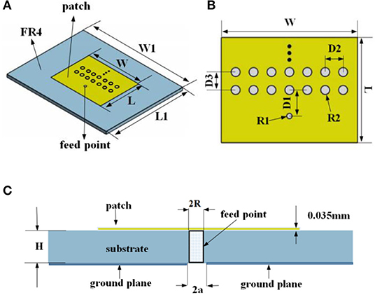
Figure 1. The structural representation of the microstrip antenna. (A) The geometry of the proposed antenna, (B) The structure of the patch, (C) The cross-section view of the coaxial feed.
The structure proposed in [26] was used as a reference in this paper, but unlike the omnidirectional calculation in [26], single direction analysis was adopted. Figure 2 shows the geometry of photonic crystals and line sources. The impressed electric line source (J0(x,y)) located at the origin O of the x-y coordinate system is sandwiched between two photonic crystals, with a separation distance of t1. A common distance in the × direction is represented by h and the distance between cylinders is d1. The structure is arranged in a periodic array. The cylindrical elements on the same layer of the array should have the same material properties and dimensions, but those on difference layers do not necessarily have to be the same. a1 is the radius of the cylinder and εr1 is relative permittivity. The number of the photonic crystal layers above the X-axis is assumed to be N1. The Y-axis is analyzed in this paper.
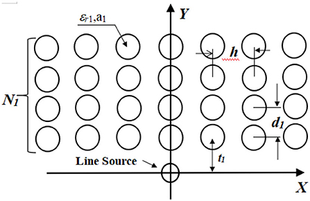
Figure 2. Scheme of a localized Y line source embedded at the origin of the coordinate system of bounded two-dimensional photonic crystals.
The conventional Floquet mode expansion method cannot be directly used since the system concerned is not periodic. Therefore, the expression of the localized line source in terms of an infinite periodic array of linearly phased line sources in the spectral domain is considered using the identity [27]:
The electric field Ez,P(x,y, ) is radiated from a periodic array of line sources defined as:
Therefore, the problem can be simplified to the calculation of the electric field Ez,P(x,y, ) radiated from the infinite periodic array of linearly phased line sources JP(x,y,
 ).
).
The primary field radiated from the periodic line sources JP(x,y, ) defined by Formula (13) is expressed using the Fourier integral representation of the Hankel function:
where k0 = 2π/λ0. The incidence of plane waves in the scattered fields can be calculated using the reflection and transmission matrices of layered periodic arrays in [28] since the primary field is expressed as a superposition of the Floquet mode. The space harmonics obtained by Formula (16) are described with the amplitude vector s( ) defined as:
As shown in Figure 3, photonic crystal layers located above the line source may be substituted by the plane boundary at y=t1. The said plane boundary is characterized by the generalized reflection and transmission matrices , whose derivation was described in [29].
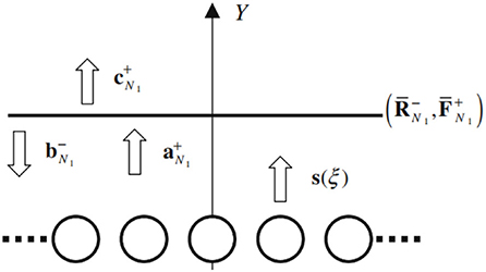
Figure 3. Multiple scattering processes of space harmonics mainly radiated from the periodic array of line sources. The plane boundary characterized by the generalized reflection and transmission matrices , takes the place of the photonic crystals.
Then, by ray tracing the orthogonal space harmonics, the following relations are obtained:
The field Ez(x,y) radiated from the localized line source (14) is obtained by plugging Formula (25) into Formula (15). A conventional numerical integration scheme is used to calculate the finite integral in Formula (15) with respect to the spectral parameter x. The singularities in the integrand are the poles that satisfy D(x) = 0, whose branch points meet κℓ(ξ) = 0. The poles correspond to the propagation constants of TE guided modes (usually limited within y < t1). The far-zone fields are obtained from the spectral response for the propagating space harmonic components as follows:
where and ϕ are the observation angles. The directive gain of the radiation G(ϕ) is given by:
The poles would degrade the radiation efficiency of the antenna and adjusting the lattice parameters of the photonic crystals could possibly eliminate the poles within the spectral range concerned. The pole removal can be easily achieved [28] by choosing the lattice parameters, enabling one of the eigenvalues η of the transfer matrix for space harmonics across the single layer of the array to satisfy |η|=1 in the far-zone radiation field. Without calculating the integration in Formula (15), the conventional asymptotic method [30] can be used to assess the contribution of the branch points. The photonic crystal array structure can significantly improve the radiation and gain of the antenna.
The through-hole structure is applied to the microstrip antenna in this paper. The equivalent circuit model of the structure with a single passing hole is shown in Figure S1, where the passing hole generates the parasitic capacitance of C and parasitic inductance of L.
The outer diameter of the through-hole is d1, the diameter of the power separation zone is d2, the thickness of FR4 is H, εr is the relative dielectric constant of the substrate, and d is the inner diameter of the through-hole.
The resonance generated between capacitance and inductance of a single hole or the resonance produced between holes will greatly affect the performance of the excitation antenna.
The series resonance formula is
The parallel resonance formula is
where f 0 is resonance frequency, ω0 is resonance angular frequency, Q is the quality factor, and R is the resistance value.
The through-hole on the antenna designed in this paper has the following characteristics:
The resonant effect between the capacitance and the inductance can improve the reflection in the antenna design. Holes also resonate with each other. The air hole in the proposed design results in the corresponding reduction of substrate material, increasing the gain of the substrate. The influence of the array hole on parameters needs parameter optimization.
The equivalent circuit model of an ordinary rectangular microstrip antenna is shown in Figure S2A, where ZS is gap impedance and Z is impedance produced by the feeding point. The equivalent circuit of a microstrip antenna with drilling holes is shown in Figure S2B, where Zk is the impedance of the hole. Figure S2C shows the resonance produced by C and L. f 0 and f 1 are not the same resonance frequency.
The resonance frequency is expressed as:
The through-hole array made from an ordinary rectangular microstrip antenna is applied to the patch of the antenna proposed in this study. Three gigahertz is taken as the reference frequency of the antenna. The antenna elements are simulated via High Frequency Simulator Structure (HFSS.15), and the return loss value is simulated by adjusting the size, spacing distance, and number of drilled holes.
First, seven through-holes are embedded into the patch according to the patch width. Then, the radius of the through-holes and the distance between holes are simulated and analyzed, as shown in Figures 4A,B. According to Figure 4A, the return loss shows little difference when R2 = 0.6 mm (23.5534 dB) and R2 = 1 mm (23.3522 dB). Thus, the radius of the holes on the designed antenna can take R2 = 1 mm. It can be seen from Figure 4B that the return loss effect is the best when D2 = 4 mm (23.3522 dB). When two rows of holes are drilled, the distance D3 should be adjusted and the value of D2 needs to be taken into account. The simulation results show that the return loss of the antenna is optimal at 2.9 GHz when D3 = 4, which is 24.3307 dB (Figure 5A).
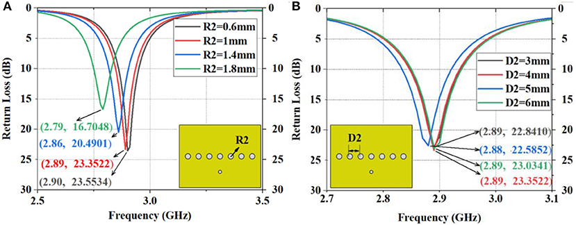
Figure 4. The simulation of return loss of the antenna with one-line drilled holes on the patch center. (A) Different dimensions of R2, (B) Different dimensions of D2.
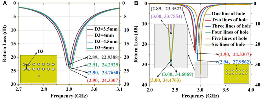
Figure 5. The simulation of D3 and different lines of drilled holes. (A) Different dimensions of D3, (B) Return loss of antenna with 1, 2, 3, 4, 5, and 6 lines of holes.
Furthermore, 1, 2, 3, 4, 5, and 6 lines of holes are drilled on antennas with R2 = 1 mm, D2 = 4 mm, and D3 = 4 mm separately, and the resulting return loss of these six kinds of antennas are compared. As shown in Figure 5B, the return loss of antennas with one-line, two-line, three-line, four-line, five-line, and six-line holes is 23.3522 dB at 2.89 GHz, 24.3307 dB at 2.90 GHz, 27.9562 dB at 2.94 GHz, 34.6069 dB at 3.00 GHz, 33.7554 dB at 3.00 GHz, and 34.4763 dB at 3.00 GHz, respectively. The simulation results of the proposed antennas with multiple drilled holes are satisfying as the return loss reaches 34.6069 dB at 3 GHz (Figure 5B). D2, D3, and R2 of the four-line structure are optimized to eliminate uncertainties, as shown in Figures 6A, 7A. The compassion between antennas with and without apertures reveals that the return loss of the designed antenna is 10.3944 dB higher than that of the antenna without apertures (Figure 7B).
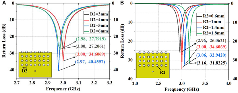
Figure 6. The simulation of return loss of the antenna with four lines of drilled holes. (A) The different dimensions of R2, (B) The different dimensions of D2.
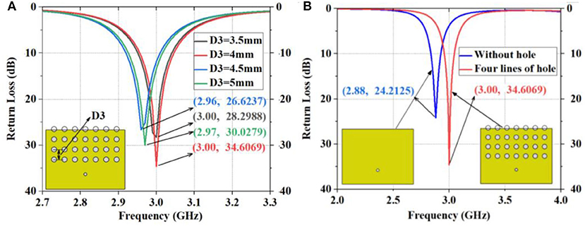
Figure 7. The simulation of D3 as well as four-line and one-line holes. (A) The different dimensions of D3, (B) Comparison between the unperforated antenna and the antenna with four-row holes.
After deciding to drill 4-line through-holes on the antenna structure, structures with square, triangular, and spherical holes are compared (Figure 8).
The comparison is made under unchanged D1, D2, and D3 in this paper, and only four rows are observed. In the one-line and two-line antennas (Figure S3), the triangle structure has better return loss. As for the three-line and four-line antennas (Figure S4), the through- hole structure has better return loss. This paper also compares the spherical holes with a radius of 0.8 mm (Figure S5). Table 1 shows the comparison of return loss between perforated antennas and the unstructured antenna. From the above analysis, antenna 10 (the four-row through-hole structure) designed in this paper is the most ideal, which verifies the above design about through-hole structures.
The above antennas with four-row holes are compared under different R2, D2, and D3 values. Some of the four-row drilled holes are on the patch and others are on the substrate. The best return loss effect is achieved at 3 GHz when R2 = 1 mm, D2 = 4 mm, and D3 = 4 mm, so the antenna with four-row holes meeting these parameters is designed. This antenna is then compared with the unperforated antenna. As shown in Figure 7B, the return loss of the designed antenna increases the output by 42.9%, when compared to the unperforated antenna, which has an overall return loss of 24.2125 dB.
The horizontal current on the surface of the patch at the TM mode with a coaxial feed coupling structure is distributed forward (please see Figure S6). The distribution of current is such that the reflection of electromagnetic waves is fine.
The return loss of the simulated antenna is 34.6069 dB and the corresponding VSWR is 1.0379. When the return loss is 10 dB, it has a 90.2 MHz bandwidth. The parameters of the proposed antenna are shown in Table 2.
As can be seen from the following figures, the simulation results of performance parameters of the designed antenna are satisfactory. Its gain is 4.9533 dBi at 3 GHz (Figure S8B), and its input impedance is about 50 Ω at 3 GHz (Figure S9B). For other simulation indicators, please see the figures in the Supplementary Materials.
Precision machining and measurements of the four-row aperture structure designed in this paper were performed. The designed antenna was processed and tested using network analyzers (CETC41, AV3629A) in a 7 × 4 × 3 m rectangular microwave darkroom in the School of Electronic Engineering of Xidian University. Before the test, the most classic two-port system error calibrator, TOSM (through, open, short, match), also known as SOLT, was used for network analyzer calibration. Before the far-field test, the tester dealt with the test environment and equipment, including instrument calibration, cable loss zeroing, turntable debugging, etc. The 50 Ω SMA connector was used for back-feed at D1 from the center of the patch. To verify the results of the simulated design, a photo of the proposed antenna prototype was taken, and its return loss was simulated and measured (Figure 9). The patch is made from copper, and the antenna surface is coated with tin to prevent oxidation. Table 3 shows the simulated and measured performance parameters of the proposed antenna with four-row holes. The measured 2-D radiation patterns (E-plane and H-plane) at 2.90, 2.95, and 3 GHz are shown in Figure 10. The simulated and measured peak gains are about 4.95 dB at 3 GHz and about 4.88 dB at 2.95 GHz, respectively. Figure 11 shows the relationship between gain and frequency when both angles are zero. The simulation and measurement results of the antenna are basically identical. According to Table 4, the parameter improvement in this paper is effective.
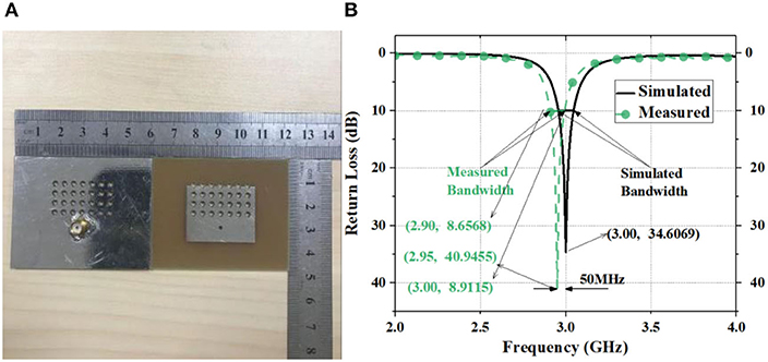
Figure 9. (A) The photo of front and back of the designed antenna; (B) simulation and measurement data of the designed antenna.

Figure 10. Measured 2-D radiation patterns at (A) 2.90GHz, (B) 2.95GHz, and (C) 3GHz (E-plane and H-plane).
As shown in Figure 9B, the difference between the measured and the simulated data is 50 MHz, which may be caused by a number of reasons. First, there are some errors between simulation and measurement. In general, the resonance frequency of the antenna after processing will be reduced, so it may lead to this situation. The HFSS software used for simulation in this study could be another reason. The method of selecting the feed and establishing the model by HFSS may be influencing factors. Third, the antenna processing accuracy, the feed welding during the test, the test cable loss in the antenna measurement, and the antenna test environment could also possibly result in the difference between the measured and the simulated data.
The process of antenna designing is subject to theoretical analysis, technical analysis, antenna design, antenna comparison, processing, and testing. This paper tries to achieve the design through theory discovery and software testing. The achieved return loss of the design is 69.1% higher than that of the antenna without holes and 18.3% higher than that of the simulated antenna. The gain increase of 58.4% is relatively non-porous. The results of this study suggest that a 4 × 7 array through-hole structure can improve the gain and radiation of microstrip antennas and can be realized based on the line source analysis and parameter optimization by using ANSYS HFSS. The simulation results are consistent with the experimental ones, even though there are some errors for the test frequency.
Innovations are made in the following four aspects: structure, theory, design optimization, and metrics improvement. First, in terms of structure, a 4 × 7 array through-hole structure is used to integrate the functions of photonic crystal and microstrip antennas. Second, theoretical analysis finds that the line source of the design structure, i.e., the 4 × 7 array hole, is different from the reference line source. The line source in a semicircle direction is also analyzed, with the corresponding formula deduced. The photonic crystal array structure can obviously improve the radiation and gain. Third, the structural design and optimization is investigated. The single-, double-, three-, four-, five-, and six-row holes are compared, and the hole spacing is explored. After design and optimization, the optimal scheme is finally determined for theoretical analysis and verification. Fourth, to improve the metrics, the 4 × 7 array structure is compared with a structure without holes. It is obvious that the return loss increases substantially. section Structural Comparison makes comparisons between several structures, which reveal that antenna 10, namely the 4 × 7 array structure, can deliver the best outcomes.
This paper promotes the research of photonic crystals and antennas and may offer help to researchers in the in-depth mining of the array hole structure in the future. This research also has some limitations. For instance, its bandwidth is not wide enough, but this issue will be improved in the future. The materials used to fabricate the prototype are low-cost, and the antenna is small in size, with easy heat dissipation and high mechanical strength. The simple structure can facilitate manufacturing and integration with other circuits. The wiring can also pass through the holes. The antenna designed in this paper can be used in the frequency band of radio navigation systems and positioning systems.
The raw data supporting the conclusions of this article will be made available by the authors, without undue reservation, to any qualified researcher.
All authors listed have made a substantial, direct and intellectual contribution to the work, and approved it for publication.
The authors would like to thank the National Natural Science Foundation of China and High-level talents program of Nanjing Forestry University for financially supporting this research under Contract Nos. 31170668 and 163070694.
The authors declare that the research was conducted in the absence of any commercial or financial relationships that could be construed as a potential conflict of interest.
The Supplementary Material for this article can be found online at: https://www.frontiersin.org/articles/10.3389/fphy.2020.00290/full#supplementary-material
1. Shackelford A, Lee KF, Chatterjee D, Guo YX, Luk KM, Chair R. Small-size wide-bandwidth microstrip patch antennas. In: IEEE Antennas and Propagation Society International Symposium. USNC/URSI (2001). p. 86–9.
3. Pozar DM. Microstrip antennas and arrays on chiral substrates. IEEE Trans Antennas Propagat. (2001) 40:86–9. doi: 10.1109/8.182462
4. Lee KF, Luk KM. Microstrip Patch Antennas. London: Imperial College Press (2011) doi: 10.1142/p669
5. Wang L, Tong J, Li Y. River Chief System (RCS): an experiment on cross-sectoral coordination of watershed governance. Front Environ Sci Eng. (2019) 13:1–3. doi: 10.1007/s11783-019-1157-9
6. Chen C, Guo Y, Wang H. Wideband symmetrical cross-shaped probe dual-beam microstrip patch antenna. IEEE Antennas Wirel Propag Lett. (2015) 14:622–5. doi: 10.1109/LAWP.2014.2375371
7. Liu S, Qi S, Wu W, Fang D. Single-feed dual-band single/dual beam u-slot antenna for wireless communication application. IEEE Trans Antennas Propagat. (2015) 63:3759–64. doi: 10.1109/TAP.2015.2438331
8. Carver K, Mink J. Microstrip antenna technology. IEEE Trans Antennas Propagat. (1981) 29:2–24. doi: 10.1109/TAP.1981.1142523
9. Lyu B, Yang Z, Gui G. Non-orthogonal multiple access in wireless powered communication networks with SIC constraints. IEICE Trans Commun. (2017) E101-B:1094–101. doi: 10.1587/transcom.2017EBP3179
10. Wang L, Jiang F, Yuan Z, Yang J, Gui G, Sari H. Mode division multiple access: a new scheme based on orbital angular momentum in millimetre wave communications for fifth generation. IET Commun. (2018) 12:1416–21. doi: 10.1049/iet-com.2017.1182
11. Chakraborty U, Kundu A, Chowdhury SK, Bhattacharjee AK. Compact dual-band microstrip antenna for IEEE 802.11a WLAN application. IEEE Antennas Wirel Propag Lett. (2014) 13:407–10. doi: 10.1109/LAWP.2014.2307005
12. Pourahmadazar J, Ghobadi C, Nourinia J, Felegari N, Shirzad H. Broadband CPW-Fed circularly polarized square slot antenna with Inverted-L strips for UWB applications. IEEE Antennas Wirel Propagat Lett. (2011) 10:369–72. doi: 10.1109/LAWP.2011.2147271
13. Islam S, Latrach M. Design construction and testing of a compact size patch antenna for RFID applications. Microwave Opti Technol Lett. (2013) 55:2920–5. doi: 10.1002/mop.27971
14. Wang W, Meng L, Ji R, Wang Z, Gao J, Liu Y, et al. A cpw-fed dual-beam shorted-patch antenna. IEICE Electron Express. (2018) 15:1–6. doi: 10.1587/elex.15.20180100
15. Shimizu N, Nagatsuma T. Photodiode-integrated microstrip antenna array for subterahertz radiation. IEEE Photonics Technol Lett. (2006) 18:743–5. doi: 10.1109/LPT.2006.871131
16. Mahdia RAH, Taha SMR. Miniaturization of rectangular microstrip patch antenna using topology optimized metamaterial. IEICE Electronic Express. (2017) 14:1–6. doi: 10.1587/elex.14.20170787
17. Boutayeb H, Denidni TA. Gain enhancement of a microstrip patch antenna using a cylindrical electromagnetic crystal substrate. IEEE Trans Antennas Propagat. (2007) 55:3140–5. doi: 10.1109/TAP.2007.908818
18. Agi K, Mojahedi M, Minhas B, Schamiloglu E. The effects of an electromagnetic crystal substrate on a microstrip patch antenna. IEEE Trans Antennas Propagat. (2002) 50:451–6. doi: 10.1109/TAP.2002.1003380
19. Lechen Y, Xiuli Z, Li H, Fu K, Zhang B. Ultra-wideband multi-frequency terahertz square microstrip patch antenna on hybrid photonic crystal substrate. J Comput Theor Nanosci. (2013) 10:968–73. doi: 10.1166/jctn.2013.2794
20. Zhu XL, Liu B. Wang X. Design of compact mems antenna based on photonic crystal structure. J Elect Eng Technol. (2019) 14:2085–90. doi: 10.1007/s42835-019-00233-7
21. Rodriguez-Berral R, Mesa F, Jackson DR. Excitation of an infinite microstrip line with a vertical coaxial feed. IEEE Trans Microwave Theor Techniq. (2008) 56:1638–48. doi: 10.1109/TMTT.2008.925568
22. El-Raouf HEA, Prakash VVS, Yeo J, Mittra R. FDTD simulation of a microstrip phased array with a coaxial feed. IEE Proc Microwaves Antennas Propagat. (2004) 151:193–8. doi: 10.1049/ip-map:20040269
23. Stutzke NA, Filipovic DS. Four-arm 2nd- mode slot spiral antenna with simple single-port feed. IEEE Antennas Wirel Propag Lett. (2005) 4:213–6. doi: 10.1109/LAWP.2005.851006
24. Pregla R. The analysis of general axially symmetric antennas with a coaxial feed line by the method of lines. IEEE Trans Antennas Propagat. (1998) 46:1433–43. doi: 10.1109/8.725274
25. Lee CS, Nalbandian V. Planar circularly polarized microstrip antenna with a single feed. IEEE Trans Antennas Propagat. (1999) 47:1005–7. doi: 10.1109/8.777124
26. Jandieri V, Yasumoto K, Toyama H. Radiation from a line source placed in two-dimensional photonic crystals. Int J Infrared Millimeter Waves. (2007) 28:1161–73. doi: 10.1007/s10762-007-9295-8
27. Lighthill MJ. Introduction to Fourier Analysis and Generalized Functions. Cambridge University Press. doi: 10.1017/CBO9781139171427
28. Yasumoto K, Toyama H, Kushta T. Accurate analysis of two-dimensional electromagnetic scattering from multilayered periodic arrays of circular cylinders using lattice sums technique. IEEE Trans Antennas Propag. (2004) 52:2603–11. doi: 10.1109/TAP.2004.834440
29. Yasumoto K, Jia H. Modeling of pfshotonic crystals by layered periodic arrays of cylinders. Electromag Theor Appl Photonic Cryst. (2005) 3:123–90. doi: 10.1201/9781315221106-3
Keywords: line source, microstrip antenna, gain, return loss, through-hole
Citation: Ding Z, Zhang D and Ma C (2020) A Study of a Microstrip Patch Antenna With a Drilled Through-Holes Array Structure Based on the Line Source Analysis Method. Front. Phys. 8:290. doi: 10.3389/fphy.2020.00290
Received: 18 January 2020; Accepted: 26 June 2020;
Published: 14 September 2020.
Edited by:
Lin Chen, University of Shanghai for Science and Technology, ChinaReviewed by:
Yuan Yao, Beijing University of Posts and Telecommunications (BUPT), ChinaCopyright © 2020 Ding, Zhang and Ma. This is an open-access article distributed under the terms of the Creative Commons Attribution License (CC BY). The use, distribution or reproduction in other forums is permitted, provided the original author(s) and the copyright owner(s) are credited and that the original publication in this journal is cited, in accordance with accepted academic practice. No use, distribution or reproduction is permitted which does not comply with these terms.
*Correspondence: Dan Zhang, emhhbmdkYW5AbmpmdS5lZHUuY24=
Disclaimer: All claims expressed in this article are solely those of the authors and do not necessarily represent those of their affiliated organizations, or those of the publisher, the editors and the reviewers. Any product that may be evaluated in this article or claim that may be made by its manufacturer is not guaranteed or endorsed by the publisher.
Research integrity at Frontiers

Learn more about the work of our research integrity team to safeguard the quality of each article we publish.