- National Engineering Laboratory for Dangerous Articles and Explosives Detection Technologies, Department of Engineering Physics, Tsinghua University, Beijing, China
We propose a graphene-based terahertz (THz) photodetector with a microstructure array designed to manipulate the surface electromagnetic modes. Benefiting from the generated localized electromagnetic resonance, a nearly perfect absorption to the incident THz radiation is observed, an asymmetrical temperature distribution is realized along the graphene channel under uniform THz illumination, and thereby an obvious photothermoelectric response is achieved. Polarization and geometry dependence of the photovoltage provides evidence that the photoresponse originated from the localized electromagnetic resonance. Our method is also suitable for other two-dimensional materials and shows promising applications for THz detection.
Introduction
Surface electromagnetic mode, excited by specific structure and material, enables extreme light confinement at subwavelength scale to localize energy in micro-nano volumes and thus can greatly enhance the interaction between electromagnetic waves and matter [1, 2]. This unique property is generally named as localized electromagnetic resonance (LER) and the resulting new-emerging phenomena have inspired a worldwide effort to investigate their intrinsic physical mechanisms [3] and explore potential applications [4, 5]. Trapped in the LER, the photons are driven to interact with the electrons and phonons accompanying a fast and massive transform of energy. A portion of energy is re-emitted back to the free space via electron oscillation. Nevertheless, a major amount of energy is dissipated in the form of heat through the processes of photon-electron scattering, electron-phonon scattering, and the ultimate lattice vibration [6]. In addition to energy waste, the accumulation of heat is also detrimental for the devices with a complex and hyperfine structure to match the surface electromagnetic mode and may cause device deformation, leading to a performance degradation and life span shortening, but few attention has been paid to this problem.
On the other hand, the heat generated in LER also provides an energy source for voltage generation, playing an important role in the photothermoelectric (PTE) effect which exhibits significant potential applications for detection of low-energy photons [7], especially for the recent high-profile terahertz (THz) range [8]. Originating from the temperature gradient across the device channel, the PTE response ΔV is highly dependent on the temperature difference ΔT across the channel as depicted by ΔV = −SΔT, where S is the Seebeck coefficient of the photoactive material [9]. Therefore, taking advantage of the unique properties of LER, i.e., the excellent light absorption and the large intensity of the localized field, the temperature gradient as well as the PTE response can be effectively enhanced [10]. Moreover, compared to the traditional PTE photodetectors in which the temperature gradient was realized by non-uniform illumination [11], spatially localized absorption in LER structures results in local heating of the channel material, allowing a uniform or even unfocused optical excitation. This strategy has been demonstrated in previous works by using conventional thermoelectric materials to construct the resonant structure. Mauser et al. reported a subwavelength grating-like thermoelectric nanostructures for resonant spectrally selective absorption, which created a large localized temperature gradient and realized a photoresponsivity of 38 VW−1 in visible range [12]. Based on guided-mode resonance effect, Monshat et al. proposed a photonic crystal resonator, achieving a narrowband visible absorptivity of 85.4% and a responsivity of 0.26 VW−1 [13]. Some other different resonant mechanisms were also employed for enhancement of the PTE response, such as the plasmonic nanostructure [14], metamaterial [15], metasurface [16], and so on [17, 18]. However, most of these former works were carried out in the infrared and visible regime, while the related research in THz band is still underexplored.
The recently emerging two dimensional materials such as graphene provides a new optoelectronic platform for developing novel functionalities, including low-energy photon detection [19] and integrated photon modulation [20]. The gapless nature brings graphene the ability in broadband absorption, making it a promising candidate for THz detection, and the bandwidth of graphene-based photodetectors can reach up to hundreds of GHz [21], as a consequence of its high carrier mobility. In addition, the electronic heat capacity of graphene is extremely low, which leads to a higher temperature rise for the same absorbed energy compared to other bulk material, highlighting its potential in acting as the channel material for PTE detectors [22]. However, limited by its petty small thickness, the absorption of graphene to the incident light is relatively weak, which is a major bottleneck in the application of graphene [23]. LER has been proved to be an important approach to enhance the interaction between matters and light [24–26]. In the LER region, several order of electromagnetic field intensity enhancement can be achieved, greatly increasing the absorption of materials. This scheme has been used to improve the absorptivity of graphene. On the other hand, LER shows great flexibility in manipulating the electromagnetic field distribution and thereby provides an effective way for constructing local absorption under uniform illumination. This feature facilitates significant application potential of LER in PTE detection, but there are still seldom works reported.
Here we develop a THz PTE detector integrated with graphene and LER microstructure. We adopt graphene as the channel material, and design a LER microstructure to enhance the absorption of graphene and produce a gradient temperature field. A sensitive and fast PTE response was observed in the proposed device under a uniform THz illumination, and characterizations of the response dependence on the microstructure geometry and THz polarization demonstrate that the PTE response is attributed to the asymmetrical field distribution induced by the LER microstructure.
Device Design and Fabrication
The device we proposed is shown in Figure 1A. The whole device was fabricated on a quartz substrate. A 200-nm thick Au with a 10-nm thick Ti adhesion layer, serving as a metal reflector, was deposited on the substrate by inductively coupled plasma chemical vapor deposition (ICPCVD), followed by growing an absorption layer of SiO2 via plasma enhanced chemical vapor deposition (PECVD). Our graphene sample was grown on a copper foil by chemical vapor deposition (CVD) and then transferred onto the SiO2 surface [27]. Oxygen plasma etching was employed to pattern the graphene into ribbons with a width of 50 μm and a period of 65 μm [28]. Finally, another 200-nm thick Au was deposited on the top, forming two electrodes located at both ends of the graphene ribbons, where one electrode comprises a resonant microstructure array with disc patterns and wires. The microstructure covers only half side of the graphene channel so as to generate an asymmetric structure.
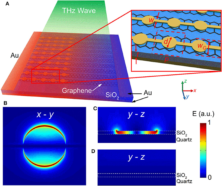
Figure 1. (A) Schematic of the graphene device with a microstructured electrode. The inset shows the geometrical parameters of the microstructure. (B) The electric field distribution in the x-y plane (at the interface between the top Au layer and free space) and (C) in the y-z plane along the central axis as the LER occurs. (D) The y-z plane electric field distribution of the side without the LER structure.
The PTE effect or the thermoelectric effect originates from the temperature gradient across the channel. Without a temperature gradient, there is no electrical potential generated between the two channel ends, whether the channel is constructed by a single material or a complex heterojunction [29]. A common strategy involves limiting the heat energy in a local area of the channel and thereby forming a gradient temperature distribution [30]. This requires that the size of the heat source (a focused light beam or a microheater) is much smaller than the channel length. However, in the THz range, the light spot diameter is generally in the order of millimeter, thus requiring a channel with the similar scale. This makes it difficult to design miniaturized and arrayed THz PTE detector. While the device proposed here can solve this problem, as shown in Figure 1A. When THz wave is incident onto the device, it will be scattered by the metal microstructure. A portion of light is scattered into free space, while the other portion is coupled into the dielectric layer, reflected by the bottom metal layer, and returns back to the interface between the top Au layer and free space. When the two portions of light recombine destructively, i.e., meet the phase matching condition, the LER occurs and the incident energy will be concentrated within the interior of the device. Figures 1B,C show the simulated electric field distribution for a single unit of the microstructure array under LER condition. It is clear that the electric field intensity near the edge of the metal disc is remarkably enhanced, and a majority of energy is retained within the SiO2 dielectric layer. Such configuration is also known as a perfect metamaterial absorber, which possesses a theoretical absorptivity close to 100% [31]. Through the LER effect, the incident photons will be effectively absorbed by the dielectric layer. The specific absorption process involves photon-electron scattering, electron-phonon scattering and phonon-phonon scattering. Finally, the incident photon energy is converted into heat in the dielectric absorber layer so as to raise the temperature of the graphene channel via thermal diffusion. Due to that the metal microstructure only partially covers the graphene channel, there is no LER generated in the uncovered side. The electric field distribution of the uncovered side is drawn in Figure 1D, and the simulation indicates that the absorptivity of this side is lower than 1%. Without LER, a majority of the incident THz wave will be reflected back into free space directly by the bottom metal layer. The interaction distance between the THz wave and the device is about twice the dielectric layer thickness and thus is too thin to absorb the light energy effectively. Therefore, the temperature of the microstructure region locally increases, while that of the other side remains low. Obviously, benefiting from the LER mechanism, a gradient temperature distribution across the channel can be established even under uniform THz illumination.
Before device fabrication, specific geometrical parameters of the microstructure need to be precisely designed. The design goal is to optimize the resonant absorption of the microstructure at a frequency of 2.52 THz, the main output frequency of our available THz source, i.e., a far-infrared gas laser (FIRL 100, Edinburgh Instruments Ltd.). Here the finite difference time domain (FDTD solutions, Lumerical) method was employed to obtain the absorption spectrum of the resonant microstructure. The conductivity of Au was set as 4.56 × 10⁷ Sm−1 [32], and the permittivity and loss tangent of SiO2 were taken as 3.84 and 0.01, respectively, which were measured by a THz time-domain spectrometer. To estimate the parameters of graphene used in the simulation, several graphene devices were fabricated in advance by the same procedure as described above. The two-dimensional conductivity was measured to be ~ 0.5 mS on average. Therefore, we set graphene as a conductive sheet with a two-dimensional conductivity of 0.5 mS in the simulation. A periodic boundary condition was used, and a y-polarization broadband THz source was incident along the –z direction. The reflectivity R of the device could be obtained directly from the simulation results, as shown in Figure 2, and then the absorptivity can be evaluated by A = 1–R.
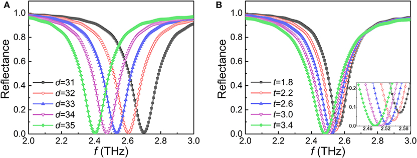
Figure 2. (A) Reflectance spectra with different t (d = 33 μm), and (B) different d (t = 2.6 μm). The other parameters are w = 3 μm and p = 65 μm. The inset in (B) is a partial enlarged view around the resonance dips.
The variable parameters of the microstructure include the disc diameter d, the periodic length p, the wire width w, and the thickness of the SiO2 dielectric layer t, as denoted in the inset of Figure 1A. Note that d and p have similar influences on the resonance since both of them determine the geometry in the horizontal plane, and the effect of w can be neglected when it is far smaller than the wavelength. Here we mainly take into account the variation of t and d, as shown in Figure 2. Determined by the practical fabrication ability, the dielectric layer thickness t was taken in the range of 2~3 μm. It can be found that the reflectance spectrum shows an obvious dip at the resonant frequency, and t has an impact on the resonant effect. The absorptivity peaks at t = 2.6 μm for 2.52 THz. While as d increases for a fixed t, the corresponding resonant frequency redshifts. When d = 33 μm, t = 2.6 μm, p = 65 μm and w = 3 μm, the LER leads to a highest absorptivity of nearly one. Considering the discrepancy introduced in practical processing and the calculation error in the simulation, a series of devices with d varying between 31 and 35 μm were fabricated. This strategy ensures that an optimal device with a LER frequency located at 2.52 THz would be achieved.
Experimental Results and Discussion
Firstly, we characterized the quality of graphene in our fabricated device. Figure 3A shows the Raman spectrum of the graphene channel excited at 633 nm, which displays two significant peaks at 1,584 and 2,641 cm−1, corresponding to the G and 2D bands, respectively. The 2D band contains only a single and sharp peak, suggesting that the graphene is monolayer [33]. Figure 3B provides the atomic force microscope (AFM) image over a selected area within the graphene channel, and Figure 3C gives an optical microscope image of the device. We can see that the graphene channel is clearly visible, and the metal structures including the LER patterns and the electrodes were also well-fabricated.

Figure 3. (A) Raman spectrum and (B) AFM image of the fabricated graphene sample, (C) Optical micrograph of the device.
Figure 4A illustrates a typical current-voltage (I-V) characteristic of our device (d = 33 μm), where its nearly linear behavior implies that the graphene channel has an ohmic contact with the electrodes. The total resistance of our device calculated from this measurement is about 1,375 Ω. Then a 2.52 THz continuous-wave radiation chopped at 330 Hz was focused onto the device, and the produced photovoltage was measured by a current amplifier (SR570, Stanford Research Systems) and a lock-in amplifier (SR830, Stanford Research Systems). All the experiments were carried out at room temperature. Figure 4B shows the generated photovoltage as a function of the power actually received by the graphene channel, calculated by Pchannel = P0 × (Achannel/Aspot), where P0, Achannel and Aspot are the incident power, the channel area and the spot area, respectively. From the slope of the linearly fitted line, we can obtain the photovoltage responsivity, whose value is RPTE = 364.4 mVW−1. The temperature difference along the channel can be estimated by dividing the PTE photovoltage by S. Here we take S as 100 μVK−1 [34, 35], which results in a temperature difference of ~10 K under a channel receiving power of 3 mW. The channel length is 600 μm, and thus the temperature gradient is ~0.016 K μm−1 along the graphene channel. This value is sensible [34, 35] and can be further improved by optimizing the LER mode. For example, the LER mode with a stronger resonance and a smaller mode volumes is preferred because such mode can limit the energy in a smaller area and lead to a higher temperature gradient. Optimizing the LER field distribution to make the localized field closer to the graphene layer is another effective way since this can reduce the energy loss in the heat conduction.
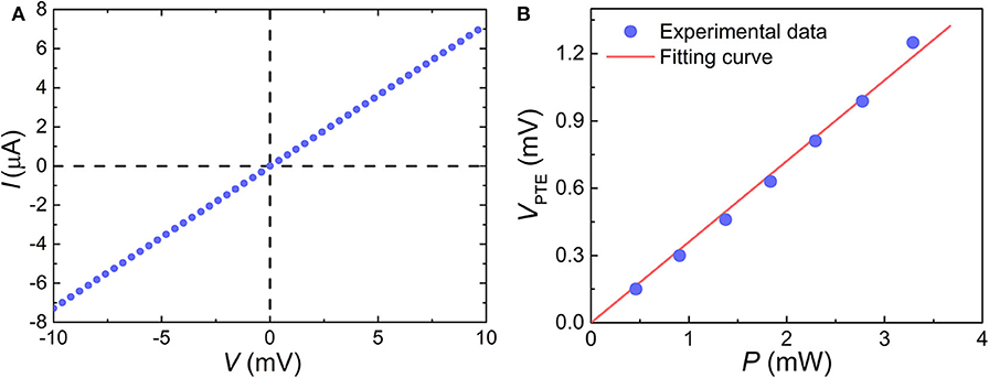
Figure 4. (A) I-V characteristic of the graphene channel, (B) Power dependence of the photovoltage under 2.52 THz illumination.
Another approach to improve the responsivity of the device is optimizing the Seebeck coefficient of the graphene channel by electrostatic doping [34–36]. For example, fabricating a top-gate electrode on the right side of the channel can allow us to tune the carrier density of graphene, as well as its Fermi level and Seebeck coefficient. In this condition, the magnitude of PTE response can be deduced by ΔV = ΔT1S1-ΔT2S2, where ΔT1 and ΔT2 are the temperature rises of the left side and the right side, and S1 and S2 are their Seebeck coefficients, respectively. When the graphene in the right side is tuned to a reverse doping type, its S value will be opposite in sign to that of the left side. The generated photovoltage in the two parts of the channel is added in series, and thus an enhanced total photovoltage would be produced.
Because the PTE effect does not need a bias, its noise voltage is mainly determined by the Johnson–Nyquist (JN) noise, and the noise equivalent power (NEP) of the device can be calculated as follows [37]:
where KB = 1.38 × 10⁻²³ JK−1 is the Boltzmann constant, T = 300 K is the environmental temperature, and R is the channel resistance of the device. The NEP of our device is 1.31 × 10⁻⁸ W Hz−1/2.
To demonstrate that PTE effect originated from the LER generated by the microstructure, the photovoltages of the devices with different metal disc diameters were measured, as given in Figure 5A. When d = 31 μm, the photovoltage is about 0.3 mV. With increasing d, the photovoltage increases to 1.3 mV at d = 33 μm and then decreases again, revealing a consistent variation tendency with the absorption shown in Figure 2A. This is because that when d = 33 μm, the resonance intensity reaches a maximum, and the absorption as well as the temperature rise are larger than that for other d values. In addition, the polarization-dependent responses were measured with a polarizer and a half-wave plate placed successively in the beam path after the THz source. Figure 5B shows the photovoltage vs. the polarization rotation angle θ of the incident THz radiation. The photovoltage is normalized to its maximum value, corresponding to the polarization perpendicular to the y-direction or the metal wires in the microstructure, defined as θ= 0°. The polarization dependent ratio is about 0.18, calculated by (Vmax−Vmin)/(Vmax+Vmin). This polarization dependence results from the polarization asymmetry of the microstructure, i.e., the existence of metal wires hampers the generation of the LER when the polarization is parallel to the wires. We also measured several devices without the LER structure and did not observe any effective response signals above the noise level, further confirming that the PTE responses is attributed to the LER mechanism.
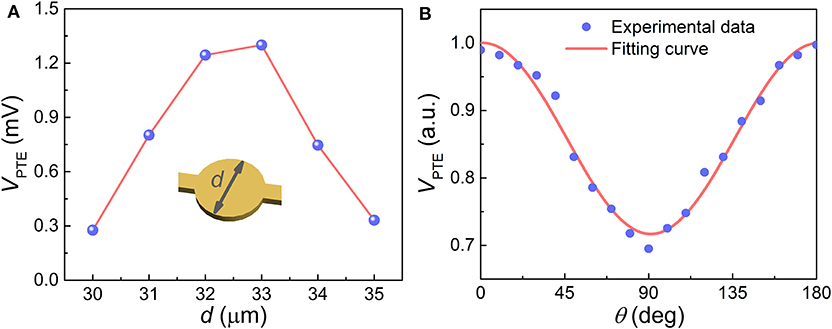
Figure 5. (A) PTE response with different metal disc diameters. (B) Polarization dependence of the photovoltage (0° degree corresponds to the polarization parallel to the y-direction), and the red curve is a sine fit of the experimental data.
The light on/off switching curve was measured with a current amplifier (SR570, Stanford Research Systems) and an oscilloscope (MSO64, Tektronix) to evaluate the response speed, as depicted in Figure 6A. By fitting the rising edge of this curve with an exponential function, the response time of our device is extracted to be 376 μs. Figure 6B shows the modulation frequency dependence of the PTE response. A similar fitting process indicates a 3 dB bandwidth of 1,765 Hz, confirming a response time in the order of submicrosecond scale. Note that the real response speed of the device may be faster than this value since the measurements here were partly limited by the bandwidth of the current amplifier. In general, the response speed of the graphene PTE detector mainly depends on two factors: the channel length and the thermal conductivity of the substrate [38]. With a shorter channel and a high thermal conductivity, the heat accumulation and diffusion over the channel can reach up to a steady state within a shorter time, indicating a faster response speed. By further optimizing the LER structure, such as reducing the period length, a shorter channel accompanying with a faster response speed can be achieved. Choosing the substrate material with a higher thermal conductivity is another strategy for improving the response speed.
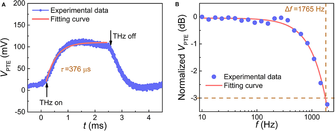
Figure 6. (A) THz on/off switching curve and (B) modulation frequency dependent response of the graphene device under 2.52 THz illumination.
Conclusion
In summary, we have proposed a novel graphene THz detector based on PTE effect enabled by the LER mechanism. The introduction of a LER microstructure enhances the absorption of graphene to THz wave and establishes a global temperature gradient across the graphene device channel even under a uniform illumination. The NEP of the detector is evaluated to be in the order of 10−8 WHz−1/2, and the response time is in the microsecond level. Further improvement of the device performance can be implemented by optimizing the resonant mode of the microstructure to reduce the mode volume, enhance the resonant strength, and concentrate more thermal energy near the graphene layer. Our scheme of LER enhanced PTE effect can be also applicable for other two-dimensional materials, possesses high compatibility with traditional microelectronic processing technology, and paves a new way for developing high-performance room-temperature THz detectors.
Data Availability Statement
The raw data supporting the conclusions of this article will be made available by the authors, without undue reservation.
Author Contributions
ZZ conceived the idea. MC and YW led the design, fabrication, and measurements of the devices and co-wrote the manuscript. All authors contributed to the article and approved the submitted version.
Funding
The authors gratefully acknowledge financial support from the National Natural Science Foundation of China (Nos. U1930109 and U1633202) and the China Postdoctoral Science Foundation (No. 2018M640121).
Conflict of Interest
The authors declare that the research was conducted in the absence of any commercial or financial relationships that could be construed as a potential conflict of interest.
References
1. Safaei A, Chandra S, Leuenberger MN, Chanda D. Wide angle dynamically tunable enhanced infrared absorption on large-area nanopatterned graphene. ACS Nano. (2019) 13:421–8. doi: 10.1021/acsnano.8b06601
2. Chen L, Xu N, Singh L, Cui T, Singh R, Zhu Y, et al. Defect-induced fano resonances in corrugated plasmonic metamaterials. Adv Opt Mater. (2017) 5:1600960. doi: 10.1002/adom.201600960
3. Xu ST, Fan F, Ji YY, Cheng JR, Chang SJ. Terahertz resonance switch induced by the polarization conversion of liquid crystal in compound metasurface. Opt Lett. (2019) 44:2450–53. doi: 10.1364/OL.44.002450
4. Chen L, Wei Y, Zang X, Zhu Y, Zhuang S. Excitation of dark multipolar plasmonic resonances at terahertz frequencies. Sci Rep. (2016) 6:22027. doi: 10.1038/srep22027
5. Cheng J, Fan F, Chang S. Recent progress on graphene-functionalized metasurfaces for tunable phase and polarization control. Nanomaterials Basel. (2019) 9:398. doi: 10.3390/nano9030398
6. Skoplaki E, Palyvos JA. On the temperature dependence of photovoltaic module electrical performance: a review of efficiency/power correlations. Sol Energy. (2009) 83:614–24. doi: 10.1016/j.solener.2008.10.008
7. Koppens FH, Mueller T, Avouris P, Ferrari AC, Vitiello MS, Polini M. Photodetectors based on graphene, other two-dimensional materials and hybrid systems. Nat Nanotechnol. (2014) 9:780–93. doi: 10.1038/nnano.2014.215
8. Wang Y, Niu Y, Chen M, Wen J, Wu W, Jin Y, et al. Ultrabroadband, sensitive, and fast photodetection with needle-like EuBiSe3 single crystal. ACS Photon. (2019) 6:895–903. doi: 10.1021/acsphotonics.8b01527
9. Suzuki D, Oda S, Kawano Y. A flexible and wearable terahertz scanner. Nat Photon. (2016) 10:809–13. doi: 10.1038/nphoton.2016.209
10. Dai W, Liang Y, Yang M, Schrecongost D, Gajurel P, Lee H, et al. Large and reconfigurable infrared photothermoelectric effect at oxide interfaces. Nano Lett. (2019) 19:7149–54. doi: 10.1021/acs.nanolett.9b02712
11. Chen M, Wang Y, Wen J, Chen H, Ma W, Fan F, et al. Annealing temperature-dependent terahertz thermal-electrical conversion characteristics of three-dimensional microporous graphene. ACS Appl Mater Inter. (2019) 11:6411–20. doi: 10.1021/acsami.8b20095
12. Mauser KW, Kim S, Mitrovic S, Fleischman D, Pala R, Schwab KC, et al. Resonant thermoelectric nanophotonics. Nat Nanotechnol. (2017) 12:770–5. doi: 10.1038/nnano.2017.87
13. Monshat H, Liu L, Lu M. A narrowband photo-thermoelectric detector using photonic crystal. Adv Opt Mater. (2018) 7:1801248. doi: 10.1002/adom.201801248
14. Shautsova V, Sidiropoulos T, Xiao X, Gusken NA, Black NCG, Gilbertson AM, et al. Plasmon induced thermoelectric effect in graphene. Nat Commun. (2018) 9:5190. doi: 10.1038/s41467-018-07508-z
15. Luxmoore IJ, Liu PQ, Li P, Faist J, Nash GR. Graphene–metamaterial photodetectors for integrated infrared sensing. ACS Photon. (2016) 3:936–41. doi: 10.1021/acsphotonics.6b00226
16. Fang J, Wang D, DeVault CT, Chung TF, Chen YP, Boltasseva A, et al. Enhanced graphene photodetector with fractal metasurface. Nano Lett. (2017) 17:57–62. doi: 10.1021/acs.nanolett.6b03202
17. Muench JE, Ruocco A, Giambra MA, Miseikis V, Zhang D, Wang J, et al. Waveguide-integrated, plasmonic enhanced graphene photodetectors. Nano Lett. (2019) 19:7632–44. doi: 10.1021/acs.nanolett.9b02238
18. Xu X, Kwon H, Gawlik B, Mohammadi Estakhri N, Alu A, Sreenivasan SV, et al. Enhanced photoresponse in metasurface-integrated organic photodetectors. Nano Lett. (2018) 18:3362–7. doi: 10.1021/acs.nanolett.7b05261
19. Lundeberg MB, Gao Y, Woessner A, Tan C, Alonso-Gonzalez P, Watanabe K, et al. Thermoelectric detection and imaging of propagating graphene plasmons. Nat Mater. (2017) 16:204–7. doi: 10.1038/nmat4755
20. Cai X, Sushkov AB, Jadidi MM, Nyakiti LO, Myers-Ward RL, Gaskill DK, et al. Plasmon-enhanced terahertz photodetection in graphene. Nano Lett. (2015) 15:4295–302. doi: 10.1021/acs.nanolett.5b00137
21. Romagnoli M, Sorianello V, Midrio M, Koppens FHL, Huyghebaert C, Neumaier D, et al. Graphene-based integrated photonics for next-generation datacom and telecom. Nat Rev Mater. (2018) 3:392–414. doi: 10.1038/s41578-018-0040-9
22. Tielrooij KJ, Massicotte M, Piatkowski L, Woessner A, Ma Q, Jarillo-Herrero P, et al. Hot-carrier photocurrent effects at graphene-metal interfaces. J Phys Condens Mat. (2015) 27:164207. doi: 10.1088/0953-8984/27/16/164207
23. Rogalski A, Kopytko M, Martyniuk P. Two-dimensional infrared and terahertz detectors: outlook and status. Appl Phys Rev. (2019) 6:021316. doi: 10.1063/1.5088578
24. Yang Y, Xu D, Zhang W. High-sensitivity and label-free identification of a transgenic genome using a terahertz meta-biosensor. Opt Express. (2018) 26:31589–98. doi: 10.1364/OE.26.031589
25. Liu W, Fan F, Chang S, Hou J, Chen M, Wang X, et al. Nanoparticles doped film sensing based on terahertz metamaterials. Opt Commun. (2017) 405:17–21. doi: 10.1016/j.optcom.2017.07.086
26. Venuthurumilli PK, Ye PD, Xu X. Plasmonic resonance enhanced polarization-sensitive photodetection by black phosphorus in near infrared. ACS Nano. (2018) 12:4861–7. doi: 10.1021/acsnano.8b01660
27. Yoo TJ, Kim YJ, Lee SK, Kang CG, Chang KE, Hwang HJ, et al. Zero-bias operation of CVD graphene photodetector with asymmetric metal contacts. ACS Photon. (2017) 5:365–70. doi: 10.1021/acsphotonics.7b01405
28. Deng T, Zhang Z, Liu Y, Wang Y, Su F, Li S, et al. Three-dimensional graphene field-effect transistors as high-performance photodetectors. Nano Lett. (2019) 19:1494–503. doi: 10.1021/acs.nanolett.8b04099
29. Wang G, Zhang M, Chen D, Guo Q, Feng X, Niu T, et al. Seamless lateral graphene p-n junctions formed by selective in situ doping for high-performance photodetectors. Nat Commun. (2018) 9:5168. doi: 10.1038/s41467-018-07555-6
30. Erikson KJ, He X, Talin AA, Mills B, Hauge RH, Iguchi T. Figure of merit for carbon nanotube photothermoelectric detectors. ACS Nano. (2015) 9:11618–27. doi: 10.1021/acsnano.5b06160
31. Landy N, Sajuyigbe S, Mock J, Smith D, Padilla W. Perfect metamaterial absorber. Phys Rev Lett. (2008) 100:207402. doi: 10.1103/PhysRevLett.100.207402
32. Shen X, Cui TJ. Photoexcited broadband redshift switch and strength modulation of terahertz metamaterial absorber. J Opt. (2012) 14:114012. doi: 10.1088/2040-8978/14/11/114012
33. Ferrari AC, Meyer JC, Scardaci V, Casiraghi C, Lazzeri M, Mauri F, et al. Raman spectrum of graphene and graphene layers. Phys Rev Lett. (2006) 97:187401. doi: 10.1103/PhysRevLett.97.187401
34. Castilla S, Terrés B, Autore M, Viti L, Li J, Nikitin AY, et al. Fast and sensitive terahertz detection using an antenna-integrated graphene pn junction. Nano Lett. (2019) 19:2765–73. doi: 10.1021/acs.nanolett.8b04171
35. Viti L, Purdie DG, Lombardo A, Ferrari AC, Vitiello MS. HBN-encapsulated, graphene-based, room-temperature terahertz receivers, with high speed and low noise. Nano Lett. (2020) 20:3169–77. doi: 10.1021/acs.nanolett.9b05207
36. Hu J, Wu T, Tian J, Klimov NN, Newell DB, Chen YP. Coulomb drag and counterflow seebeck coefficient in bilayer-graphene double layers. Nano Energy. (2017) 40:42–8. doi: 10.1016/j.nanoen.2017.07.035
37. Zak A, Andersson MA, Bauer M, Matukas J, Lisauskas A, Roskos HG, et al. Antenna-integrated 0.6 THz FET direct detectors based on CVD graphene. Nano Lett. (2014) 14:5834–8. doi: 10.1021/nl5027309
Keywords: photothermoelectric effect, THz, localized electromagnetic resonance, graphene, detector
Citation: Chen M, Wang Y and Zhao Z (2020) Localized Electromagnetic Resonance Enabled THz Photothermoelectric Detection in Graphene. Front. Phys. 8:216. doi: 10.3389/fphy.2020.00216
Received: 22 March 2020; Accepted: 20 May 2020;
Published: 30 June 2020.
Edited by:
Lin Chen, University of Shanghai for Science and Technology, ChinaReviewed by:
Li Tao, The Chinese University of Hong Kong, ChinaYaping Dan, Shanghai Jiao Tong University, China
Copyright © 2020 Chen, Wang and Zhao. This is an open-access article distributed under the terms of the Creative Commons Attribution License (CC BY). The use, distribution or reproduction in other forums is permitted, provided the original author(s) and the copyright owner(s) are credited and that the original publication in this journal is cited, in accordance with accepted academic practice. No use, distribution or reproduction is permitted which does not comply with these terms.
*Correspondence: Ziran Zhao, emhhb3pyQHRzaW5naHVhLmVkdS5jbg==
 Meng Chen
 Yingxin Wang
 Ziran Zhao