 Alireza Kargar*Huicong HongJoshua TowerAndrey GueorguievHadong Kim
 Leonard CirignanoJames F. Christian
 Michael R. SquillanteKanai Shah
- Radiation Devices Inc. (RMD), Watertown, MA, United States
Lithium indium selenide (LiInSe2) is being developed for use as a room temperature semiconductor detector for thermal neutrons. The material has been studied for a number of applications including non-linear optics such as parametric oscillators, as anode material for lithium ion batteries, piezoelectrics, as a scintillation detector material, and as a semiconductor detector material. The recent advances of the crystal growth, material processing, and detector fabrication have led to semiconductor neutron detectors with up to 100 mm2 active area. The theoretical thermal neutron detection sensitivity and gamma rejection ratio (GRR) are comparable to 10 atm, 3He tubes of similar size. Detector fabrication and characterization are described and the results are discussed.
Introduction
Semiconductors with one or more constituent neutron sensitive isotopes have potential for compact, efficient thermal neutron detection [1]. Table 1 shows neutron sensitive isotopes with relatively high thermal neutron interaction cross sections along with reaction products and energies. Reactions that yield charged particles with ranges much shorter than the semiconductor dimensions are desired for neutron detection. Unlike conversion layered devices, the detection efficiency of semiconductor devices that incorporate thermal neutron sensitive isotopes as a constituent would not be limited by the short range of charged particle reaction products in the converter layer. In this paper, we report on LiInSe2 semiconductors for thermal neutron as well as its capability for pulse height gamma-ray rejection.
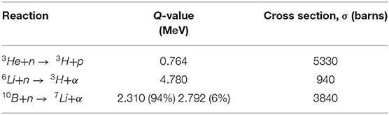
Table 1. The thermal neutron reaction and the corresponding Q-values and absorption cross sections.
LiInSe2 has a wide bandgap and high resistivity, allowing for detectors for room-temperature operation with low noise (low leakage current) [2]. Several crystals of LiInSe2 with varying conditions were grown and characterized. The optical transmission spectroscopy measurement along with resistivity measurement were performed on many LiInSe2 samples and the results are reported for one representative sample. A moderated 241AmBe fast neutron source was used as the source for thermal neutrons to investigate the device neutron response. Further, the gamma-ray response to 60Co source was measured and the results of the neutron/gamma-ray response are reported.
Calculated Absorption
The reactions used in traditional neutron detectors are listed in Table 1. Considering the Q-value listed in Table 1, the 6Li(n,α)3H reaction gives off charged particles with higher energy, resulting in better neutron-gamma ray discrimination. 6Li has the highest thermal neutron absorption cross section (940 barns) in 6LiInSe2 composition, which makes the macroscopic thermal neutron absorption cross section of 6LiInSe2 composition relatively high. This cross section can be evaluated from the basic relations (labeled as Equation 1) as:
where for a given material composition, Σ is the macroscopic thermal neutron absorption cross section of the composition in cm−1, σtot is the summation of microscopic thermal neutron absorption cross sections of all elements in the composition in barns (σtot = σLi + σIn + 2σSe), ρ is the density of the composition in grams per cm3, Na is the Avogadro's number and A is the molecular weight of the composition in grams per mole. If 100% of lithium atoms are 6Li in 6LiInSe2 compound, Σ can be evaluated as 11.2 cm−1 [3, 4], given density of 4.47 g cm−3 for the compound and the microscopic thermal neutron absorption cross section of the elements, σ, as: 940 barns for 6Li atoms, 193.8 barns for indium atoms and 11.7 barns for Se atoms. Note that, only the 6Li(n,α)3H reaction gives off charged particles for the detection application and has the highest absorption cross section among all elements of the composition. The thermal neutrons that interact with In and Se atoms are absorbed in the composition but are not detected. Based on the 11.2 cm−1 absorption cross section, a 2.0 mm thick 6LiInSe2 crystal absorbs 89% of the thermal neutrons (intrinsic absorption efficiency) based on the following relation (labeled as Equation 2), where t is the thickness of the crystal in cm:
The contribution from 6Li to the absorbed thermal neutrons is: (= 0.82). In other words 82% of the total absorbed thermal neutrons will experience the 6Li(n,α)3H reaction, and can be detected. In comparison, a 2.0 mm thickness of 3He at 10 atm absorbs only 32% of thermal neutrons, which is based on macroscopic thermal neutron absorption cross section of 1.9 cm−1 for 3He at 10 atm based on Equation (1) or Scattering Length Density Calculator [3].
Experimental Procedure
Crystal Growth
6LiInSe2 crystals were grown by the Vertical Bridgman (VB) technique, following methods described in the literature [2, 5–7]. Semiconductor grade high-purity indium and selenium were purchased from Sigma-Aldrich. Enriched 6Li was obtained from the Y-12 Isotope office at Oak Ridge National Laboratory in Oak Ridge Tennessee. The LiInSe2 was synthesized in two steps: first by reaction of lithium metal with indium metal in the melt at 1,000°C contained in a pBN crucible, which is sealed under vacuum in a larger quartz ampoule along with selenium beads at the bottom of the ampoule. Selenium vapor reacts with lithium-indium molten alloy to form LiInSe2. LiInSe2 crystals are then grown in the same pBN crucible using the vertical Bridgman crystal growth method in a 2-zone Mellon furnace. Figure 1 shows an ingot removed from the growth ampoule. As can be seen in the figure, the crystal has a chartreuse-yellow color. Note that the voids, on the surface of the ingot, are due to bubbles that form on the surface during the melting of the Li and In metals.

Figure 1. 6LiInSe2 ingot (G77) after crystal growth.
Detector Fabrication
Once the LiInSe2 crystals were taken out of the ampoule, they were cut, and polished. The polished crystals had average final thickness of 0.7 mm. The samples were cleaned with cyclohexane prior to contact deposition. Optical transmission measurements were performed at this stage on the samples, as will be discussed later. Iron was deposited as the metal contacts (typical thickness of 500 angstroms and 8 mm in diameter) on both sides of each sample through thermal evaporation. Carbon paste was used to attach 0.05 mm (2 mil) Pd wires to the Fe contacts. Note that Au, Cr, and Pt have also been previously used and all metals have shown good performances. Fe, however, was the most stable of the metals for the longevity of the LiInSe2 detectors. In other words, the detector was not degraded over time. The samples were then mounted on ceramic substrates using RTV Si based glue for further characterization. Figure 2 shows the detector, labeled as 6LiInSe2-G77-6, fabricated from ingot G77. Thirty eight samples were fabricate and tested from different ingots; data for one representative 6Li enriched detector is reported in this paper.
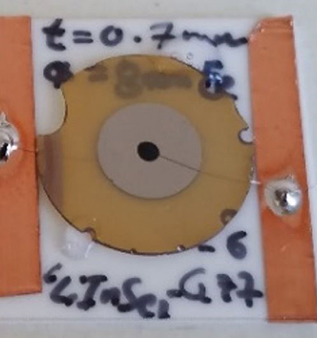
Figure 2. The fabricated planar detector from ingot G77 (labeled as 6LiInSe2-G77-6) with 0.7 mm thickness and 8 mm Fe contact diameter. The sample is wired using 2 mil Pd wire attached to Fe contacts on both side with carbon paste. The planar detector is mounted on a 1 square inch ceramic substrate using RTV Si based glue.
Table 2 shows data from 38 devices fabricated from wafers cut from eleven LiInSe2 crystal ingots. The data include the optical transmission spectra, resistivity, and the neutron and gamma-ray response. The bandgap was estimated from the transmission spectra for five samples to be 2.82–2.86 eV. All 38 eight samples were similar in color. Devices were tested with a variety of electrode materials including Cr/Au, Fe, Fe/Au, conducting polymer, and Fe/Polymer. Iron electrodes provided the best stability. Resistivity calculated from IV data ranged from about 1 × 10¹¹ to 6 × 10¹²Ω-cm Thirty six of the detectors detected both gamma rays and neutrons.
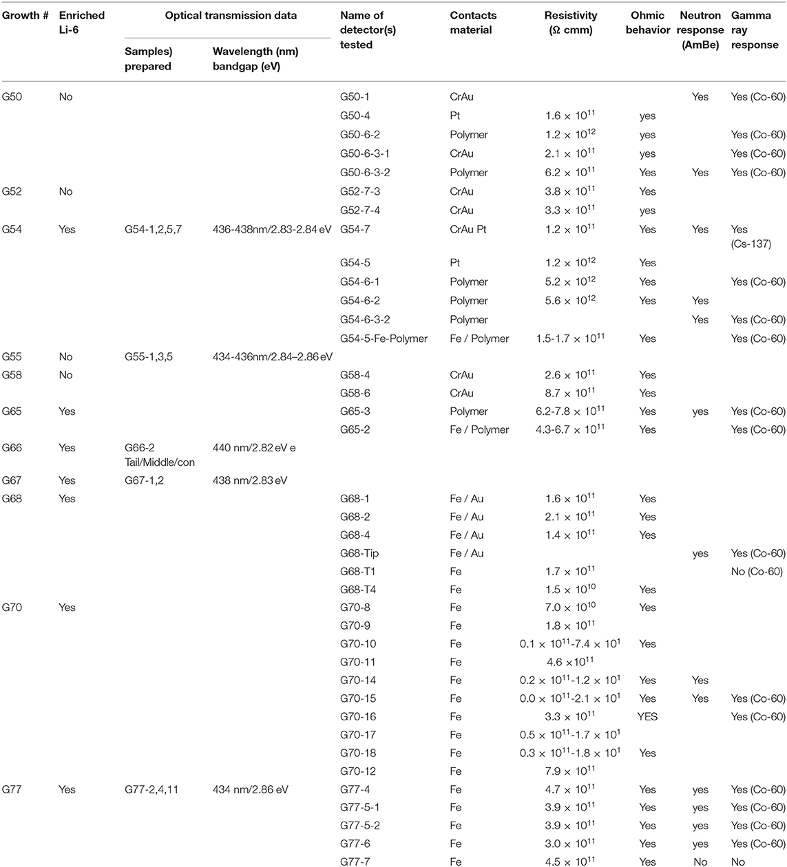
Table 2. Characteristics of LiInSe2 crystals and devices.
Detector Characterization
Three measurements were employed for characterization of the samples: current-voltage (I-V) measurements, optical transmission measurements, and pulse height spectrum measurements (neutrons and gamma rays). Optical transmission from 400 to 800 nm was conducted at room temperature using a Cary spectrometer. The results of the optical transmission spectroscopy measurements are presented in Results section. A programmable Keithley current-voltage (I-V) characteristic measurement system was used to monitor and record the current at different biases. A linear behavior was observed for both forward and reverse bias, indicating ohmic behavior of Fe/LiInSe2 interface. The values for the resistivity along with the I-V characteristic curve for one of the samples is presented below.
A Tennelec high voltage power supply (HVPS), a CR-110 Cremat preamplifier, a CANBERRA 2022 amplifier and a multi-channel analyzer (MCA) were used to monitor and acquire pulse height. The top contact of the detectors was grounded and the bottom contact was positively biased at +300 V through the preamplifier. The amplifier gain was set to 210×, 8 μs shaping time and positive polarity. The test box with detector, connections, and sources for neutron/gamma-ray counting measurements is shown in Figure 3. With the above mentioned setup, pulse height spectra were collected from all samples with a moderated 241AmBe neutron source and 60Co gamma-ray source. Note that the 241AmBe neutron source has a custom designed casing as illustrated in Figure 4 to facilitate the thermalization of neutrons leaving the bottom of the casing. The schematic of the measurement setup is shown in Figure 5. The results of device response to neutrons and gamma rays are reported below.
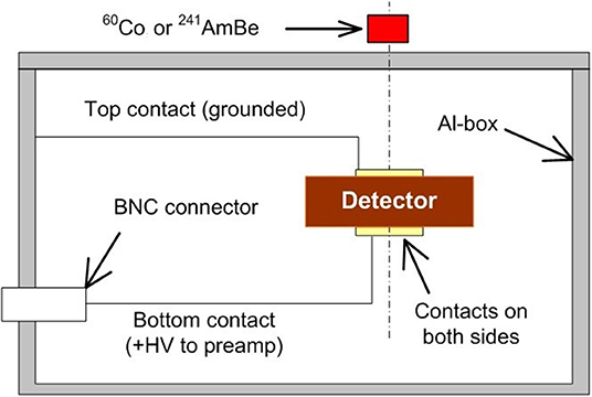
Figure 3. Schematic of test setup with 241AmBe neutron source and 60Co gamma-ray source.
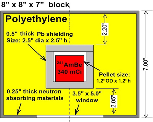
Figure 4. The RMD custom designed casing for the 241AmBe neutron source. The source holder geometry is designed in a way that most of the fast neutrons are thermalized by the polyethylene (as moderator) before reaching the detector. The “dia.” on the figure is the acronym for diameter.
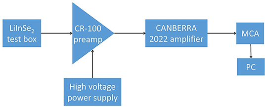
Figure 5. Schematic of the detector test circuit.
Results
Optical Transmission and Spectroscopy Results
The results of the optical transmission measurements for three samples of ingot G77 are presented in Figure 6. The absorption edge was observed at about 434 nm, which corresponds to an energy bandgap of 2.86 eV for LiInSe2 crystals.
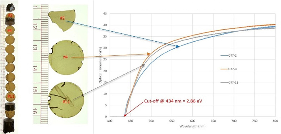
Figure 6. Optical transmission spectra for 0.7 mm thick LiInSe2 crystals sliced from ingot G77. The estimated bandgap is at 434 nm, equivalent to 2.86 eV.
Resistivity Results
The current-voltage (IV) characteristic curve obtained from one of the planar devices in Table 2 (6LiInSe2-G77-6 fabricated from G77 ingot) is presented in Figure 7. Note that, this is one of the representatives of the 38 fabricated devices listed in Table 2, and one of the 17 devices fabricated with Fe contacts on both sides of the device. As shown, the resistivity of the 6LiInSe2-G77-6 sample was determined to be 3.0 × 10¹¹ Ω cm. Note that the IV curve shows a very linear ohmic behavior. It is known that formation of ohmic contact for a metal-semiconductor interface depends on, the work function WF of metal (Fe in this case being 4.5 eV) and the bandgap of semiconductor (2.86 eV for LiInSe2), the electron affinity of semiconductor and the position of Fermi level within the bandgap (p-type of n-type semiconductor). This ohmic behavior was also observed for other metals applied to LiInSe2 material. Those metals are Au (WF = 5.3 eV), Pt (WF = 5.5 eV) and Cr (WF = 4.5), all forming ohmic contacts on LiInSe2 materials, based on the RMD database summarized in Table 2.
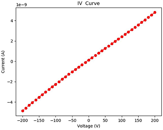
Figure 7. Current-voltage (IV) characteristic curve for 6LiInSe2-G77-6 sample. The resistivity of the sample is evaluated to be 3.0 × 10¹¹ Ω cm, for the sample with 0.7 mm thickness and 8 mm Fe contact diameter.
Neutron and Gamma-Ray Counting Results
Figure 8 shows spectra for background, 241AmBe neutron source and 60Co gamma-ray source with 6LiInSe2-G77-6 detector. The spectra were taken in 1 h increments with the detector under continuous bias for 21 h to examine the stability over time.
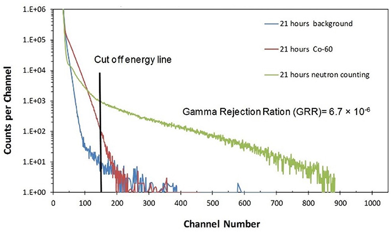
Figure 8. Neutron, gamma-ray, and background spectra of 241AmBe and 60Co obtained over a 21-h period under continuous bias using 6LiInSe2-G77-6 sample with Fe contacts. The cut off energy line was chosen to be around channel 150, close to endpoint of 60Co gamma ray energy line. The GRR was estimated to be around 1.94 × 10⁻⁶ for 6LiInSe2-G77-6.
Discussion
Gamma Rejection Ratio (GRR) is defined as the difference of the gamma-ray (γ) counts and background (BG) above the cut off energy line, over the total counts of gamma rays. Thus, GRR can be written as:
The cut off energy line was chosen to be around channel 150, close to the endpoint of 60Co gamma ray energy line. The line is shown for the combined spectra for the 241AmBe/60Co neutrons and gamma-rays, and the background for 21 h, as shown in Figure 8. By integrating the counts and using the equation above, the GRR was estimated to be around 6.7 × 10⁻⁶ for 6LiInSe2-G77-6 sample. The GRR is an important ratio for thermal neutron devices since it indicates the device capability in rejecting the gamma rays, while still detecting the thermal neutrons above the cut off energy line.
Conclusion
LiInSe2 semiconductor devices were successfully fabricated and tested for thermal neutron detection purposes. The devices showed response to neutrons emitted from a thermalized 241AmBe source, with decent Gamma Rejection Ratio (GRR) of 6.7 × 10⁻⁶. A compact solid state neutron detection system based on LiInSe2 would be a major breakthrough over conventional thermal neutron detectors, such as 3He tubes that are currently in short supply. This is the long term goal for this study at RMD Inc. Other goals for this research are improving the crystal quality and scaling up the device size. It should be noted that in recent years, other groups have conducted research on Li-based semiconductor devices for thermal neutron detection applications [8–11].
Data Availability Statement
The datasets analyzed in this article are not publicly available. Requests to access the datasets should be directed to Dr. Kanai Shah (kshah@rmdinc.com), since they may contain proprietary information.
Author Contributions
All authors listed have made a substantial, direct and intellectual contribution to the work, and approved it for publication.
Conflict of Interest
The authors of this article were employed by company Radiation Devices Inc. (RMD).
The authors declare that the research was conducted in the absence of any commercial or financial relationships that could be construed as a potential conflict of interest.
Acknowledgments
This work has been supported by the US Department of Homeland Security, Countering Weapons of Mass Destruction Office, under competitively awarded contracts HSHQDC-11-C-00061 and HSHQDC-16-C-00001. This support does not constitute an express or implied endorsement on the part of the Government.
References
1. McGregor DS, Unruh TC, McNeil WJ. Thermal neutron detection with pyrolytic boron nitride. Nucl Instrum Meth A. (2008) 591:530. doi: 10.1016/j.nima.2008.03.002
2. Guo L, Xu Y, Zheng H, Xue W, Dong J, Zhang B, et al. Stoichiometric effects on the photoelectric properties of LiInSe2 crystals for neutron detection. Cryst Growth Des. (2018) 18:2864. doi: 10.1021/acs.cgd.7b01705
3. NIST Center for Neutron Research. Available online at: http://www.ncnr.nist.gov/resources/n-lengths (accessed May 26, 2011).
4. Kargar Tower J, Hong H, Cirignano L, Higgins W, Kanai Shah. Lithium and boron based semiconductors for thermal neutron counting. Proc SPIE. (2011) 8142:81421P. doi: 10.1117/12.899363
5. Isaenko L, Yelisseyev A, Lobanov S, Petrov V, Rotermund F, Slekys G, et al. LiInSe2: A biaxial ternary chalcogenide crystal for nonlinear optical applications in the midinfrared. Appl Phys. (2002) 91:9475. doi: 10.1063/1.1478139
6. Kamijoh T, Kuriyama KJ. Single crystal growth and characterization of LiInSe2. Cryst Growth. (1981) 51:6. doi: 10.1016/0022-0248(81)90003-8
7. Chica DG, He Y, McCall KM, Chung DY, Pak RO, Trimarchi G, et al. Direct thermal neutron detection by the 2D semiconductor 6LiInP2Se6. Nature. (2020) 577:346. doi: 10.1038/s41586-019-1886-8
8. Tupitsyn E, Bhattacharya P, Rowe E, Matei L, Groza M. Single crystal of LiInSe2 semiconductor for neutron detector. Appl Phys Lett. (2012) 101:202101. doi: 10.1063/1.4762002
9. Stowe AC, Woodward J, Tupitsyn E, Rowe E, Wiggins B, Matei L, et al. Lithium-containing semiconductor crystals for radiation detection. J Cryst Growth. (2013) 379:111. doi: 10.1557/opl.2013.1145
10. Stowe AC, Cochran J, Bhattacharya P, Tupitsyn E, Wiggins B, Groza M, et al. Lithium-containing semiconductor crystals for radiation detection. Proc MRS. (2013) 1576. doi: 10.1557/opl.2013.1145
Keywords: enriched Li, 6Li, thermal neutron detection, detector, LiInSe2, semiconductor and lithium indium selenide
Citation: Kargar A, Hong H, Tower J, Gueorguiev A, Kim H, Cirignano L, Christian JF, Squillante MR and Shah K (2020) LiInSe2 for Semiconductor Neutron Detectors. Front. Phys. 8:78. doi: 10.3389/fphy.2020.00078
Received: 28 October 2019; Accepted: 05 March 2020;
Published: 09 April 2020.
Edited by:
Paul Sellin, University of Surrey, United KingdomReviewed by:
Amir Bahadori, Kansas State University, United StatesBin-Bin Zhang, Northwestern Polytechnical University, China
Copyright © 2020 Kargar, Hong, Tower, Gueorguiev, Kim, Cirignano, Christian, Squillante and Shah. This is an open-access article distributed under the terms of the Creative Commons Attribution License (CC BY). The use, distribution or reproduction in other forums is permitted, provided the original author(s) and the copyright owner(s) are credited and that the original publication in this journal is cited, in accordance with accepted academic practice. No use, distribution or reproduction is permitted which does not comply with these terms.
*Correspondence: Alireza Kargar, YWthcmdhckBybWRpbmMuY29t