 David Z. Gao
 Jack Strand
 Manveer S. Munde
 Alexander L. Shluger
94% of researchers rate our articles as excellent or good
Learn more about the work of our research integrity team to safeguard the quality of each article we publish.
Find out more
ORIGINAL RESEARCH article
Front. Phys., 29 March 2019
Sec. Chemical Physics and Physical Chemistry
Volume 7 - 2019 | https://doi.org/10.3389/fphy.2019.00043
This article is part of the Research TopicThe Role of Non-Stoichiometry in the Functional Properties of Oxide MaterialsView all 14 articles
Dielectric oxide films in electronic devices undergo significant structural changes during device operation under bias. These changes are usually attributed to aggregation of oxygen vacancies resulting in formation of oxygen depleted regions and conductive filaments. However, neutral oxygen vacancies have high diffusion barriers in ionic oxides and their interaction and propensity for aggregation are still poorly understood. In this paper we briefly review the existing data on static configurations of neutral dimers and trimers of oxygen vacancies in technologically relevant SiO2 and HfO2 and then provide new results on the structure and properties of these defects in amorphous SiO2 and HfO2. These results demonstrate weak interaction between neutral O vacancies, which does not explain their quick aggregation. We propose that trapping of electrons, injected from an electrode, by the vacancies may result in creation of new neutral vacancies in the vicinity of pre-existing vacancies. We describe this mechanism in a-SiO2 and demonstrate that this process becomes more efficient as the vacancy clusters grow larger.
Crystalline and amorphous SiO2 and HfO2 are important materials for microelectronics as dielectric layers in transistors and memory cells, fiber optics, mirror coatings, resistive random access memory (ReRAM), and neuromorphic cells (see [1–3]). Under an applied stress bias, field-effect transistors (FETs) experience a gradual increase in gate leakage, noise signal, threshold voltage shift, decrease of trans-conductance, and other degradation effects, which are accelerated by strong bias and may lead to dielectric breakdown [1, 4]. These effects have generally been attributed to defect generation and aggregation in oxide layers [1, 4, 5]. The creation of new defects is associated with structural changes in the oxide and requires significant energy [1, 6, 7]. In particular, the aggregation of oxygen vacancies as a result of electrically stressing sub-stoichiometric amorphous SiOx (x = 1.32) films is thought to facilitate the dielectric breakdown of complementary metal-oxide-semiconductor (CMOS) devices [8–10] and electroforming in resistive random access memory cells [3, 11, 12]. However, the fundamental atomistic mechanisms behind these processes are still poorly understood. Both the creation of additional oxygen vacancies and the interaction of diffusing vacancies have been proposed as mechanisms for vacancy aggregation.
Clustering of O vacancies is known to occur in the bulk and at surfaces of reducible oxides, such as e.g., TiO2 [13, 14], CeO2 [15, 16], and SrTiO3 [17]. It is much less understood in nonreducible wide band gap oxides, such as MgO, SiO2, and HfO2. The formation of pairs of O vacancies has been suggested in heavily thermochemically reduced MgO [18]. Recent simulations [19, 20] have shed some light on the formation of O-vacancy clusters in SiO2 and HfO2. Computational modeling was used to investigate the structures and binding energies of vacancy dimers and trimers in amorphous (a)-SiO2, the energy barriers for the diffusion of individual vacancies, and whether this diffusion can be stimulated by trapping of injected electrons at vacancies [19]. The calculations of di- and tri-vacancy clusters demonstrate that there are favorable sites for vacancy aggregation in a-SiO2 with maximum binding energies of approximately 0.13 and 0.18 eV, respectively. However, an average neutral vacancy diffusion barrier was calculated to be 4.6 eV [19], rendering the clustering of randomly distributed neutral vacancies via diffusion unfeasible.
The calculations performed in Bradley et al. [20] demonstrate that the formation of neutral oxygen vacancy dimers, trimers and tetramers in monoclinic HfO2 is accompanied by an energy gain with respect to the separated vacancies, which depends on the size and shape of the aggregate. In the most strongly bound configurations, vacancies are unscreened by Hf cations and form voids within the crystal, with the larger aggregates having larger energy gain per vacancy (0.11–0.18 eV). The negatively charged di-vacancy was found to have similar binding energies to the neutral one, while the positively charged di-vacancy was found to be unstable. Thus, the aggregation process of either neutral or negatively charged oxygen vacancies in m-HfO2 is energetically feasible. However, the energy barrier for the diffusion of neutral O vacancies is about 2.4 eV [21], again suggesting that aggregation of vacancies via diffusion processes is too slow to explain e.g., electroforming in HfO2 films.
The realization that the formation of oxygen vacancy clusters in a-SiO2 and m-HfO2 via thermally activated diffusion is inefficient implies that an alternative mechanism should be responsible for the aggregation of oxygen vacancies under electrical stress. In particular, O-vacancy aggregation could result from creation of new vacancies near the pre-existing vacancies. To achieve that, an O atom should be displaced from its lattice position to an interstitial site, creating an O-vacancy at the original site and an interstitial O ion, i.e., a Frenkel defect pair.
To put this mechanism in the context of previous studies, we briefly review the structure and characteristics of vacancy dimers and trimers in a-SiO2 and crystalline and a-HfO2. We then discuss the mechanisms of Frenkel defect creation in SiO2 and HfO2 facilitated by electron injection and show how similar mechanisms can produce new O-vacancies in the vicinity of pre-existing O-vacancies on the example of a-SiO2. We demonstrate that two electrons trapped at a pre-existing O-vacancy facilitate the formation of a new O-vacancy and an interstitial O2− ion and that this process becomes more probable as the vacancy clusters grow larger.
The initial non-defective amorphous structures of SiO2 and HfO2 were obtained using classical molecular dynamics and a melt and quench procedure, which is described in detail in prior publications [22, 23]. DFT was then used to optimize starting amorphous geometries, calculate their electronic structures, and study the properties of neutral and charged O defects in the material. Ten periodic models of a-SiO2 containing a total of 216 atoms each were produced using the ReaxFF force-field [24, 25] implemented in the LAMMPS code [26] and an NPT ensemble. ReaxFF was selected because it was originally parameterized to reproduce the properties of small clusters and silica polymorphs [24, 25] and reproduces the structural characteristics of silica glass well [27]. The initial models of a-HfO2 structures were created using the pair potentials [28] and the LAMMPS package [26]. Nine periodic models of a-HfO2, each containing 324 atoms, have been generated using classical molecular dynamics and a melt and quench procedure in an NPT ensemble. The Berendsen thermostat and barostat were used to control the simulations. The melt cooling rates were 8 and 0.75 K/ps for SiO2 and HfO2, respectively. We note that using an NPT ensemble creates distribution of densities of amorphous samples. In this work we used densities corresponding to experimental samples, as discussed in El-Sayed et al. [22] and Kaviani et al. [23].
Most DFT calculations were performed using the Gaussians and Plane Waves [29] method as implemented in the CP2K code [30]. The PBE0-TC-LRC [31] nonlocal functional was selected to accurately reproduce the band gap of a-SiO2 and used in conjunction with the auxiliary density matrix method (ADMM) [32] to mitigate the computational expense. Finally, we used the MOLOPT basis set [33] along with the corresponding pseudopotentials (GTH) [34] and a 400 Ry plane wave cutoff. This method predicts an average band gap of 8.1 eV for amorphous SiO2. The densities, radial distribution functions, distributions of Si-O bonds and Si-O-Si angles, as well as neutron structure factors of a-SiO2 models used in this work have been evaluated in El-Sayed et al. [22] and showed good agreement with prior theoretical [27, 35] and experimental [36] studies. This analysis demonstrated that these amorphous models are able to produce disordered continuous random networks that accurately represent the structure of a-SiO2.
The densities of the DFT optimized a-HfO2 structures used in this work are in the experimentally determined range of 9.6 – 9.7 g cm3 [23]. Contrary to a-SiO2, a-HfO2 samples are characterized by distributions of coordinations of Hf and O ions and bond lengths. In particular, around 56% of the Hf atoms are bonded to 6 oxygen atoms, 38% are bonded to 7, and 6% to 5 oxygen atoms. On the other hand, 83% of the oxygen atoms are 3 coordinated, and there are about 6% of 2 coordinated oxygen atoms. These are in good agreement with previous studies, as discussed in detail in Kaviani et al. [23]. The one-electron band gap of initial structures does not contain localized states due to under-coordinated atoms and the band gap determined as a difference between the energies of HOMO and LUMO Kohn-Sham (K-S) energies is equal to 6.0 eV on average (ranging from 5.8 to 6.2 eV in different structures).
The formation energy of a vacancy was calculated using the standard formula
where EVac and EBulk are the total energies of the vacancy and pure cell, respectively. μO is the chemical potential of oxygen, q is the charge state of the vacancy, and EFermi is the Fermi level referenced to the energy eigenvalue of the valence band maximum, EVBM. When modeling charged vacancies, charge corrections due to the interaction of periodic images were evaluated using the Lany and Zunger method [37, 38], with a dielectric constant of 3.9 for a-SiO2 and 20 for a-HfO2, and a Madelung constant of 2.8373 for the cubic cells. The population analysis of electronic states was carried out using the Bader method [39]. For the sake of convenience, all charges will be given in units of electron charge.
As observed consistently in previous work, the removal of an oxygen atom results in the formation of a Si-Si bond at the vacancy site ranging from 2.20 to 2.80 Å in length [19, 40–43]. This creates a doubly occupied defect state within the band gap between 0.39 and 1.34 eV above the valence band maximum (VBM), with the LUMO also positioned within the band gap between 7.04 and 8.20 eV above the VBM [40, 42]. However, such data with regards to di- and tri-vacancy clusters has not been previously published.
In the current study, we have analyzed a total of 25 di-vacancy structures and 12 tri-vacancy clusters using the sampling method described in detail in Munde et al. [19]. Typical configurations of di- and tri-vacancies in a-SiO2 are shown in Figure 1. As illustrated, an oxygen tri-vacancy can exhibit three possible configurations: (i) the three vacancies are situated within a 3-member ring; (ii) the three vacancies diverge from a central Si atom to give a “Y” configuration; and (iii) the three vacancies form a chain. Our previous results have suggested that the 3-member ring and Y-geometry are energetically favorable when compared to the vacancy chain [19]. In all cases, the removal of additional oxygen atoms results in further network distortion. Si-Si bond lengths range from 2.20 to 3.00 Å and 2.40 to 3.00 Å in di- and tri-vacancy clusters, respectively. One can attribute the increase in the lower limit to bond length to a decrease in atomic density around the vacancy cluster site.
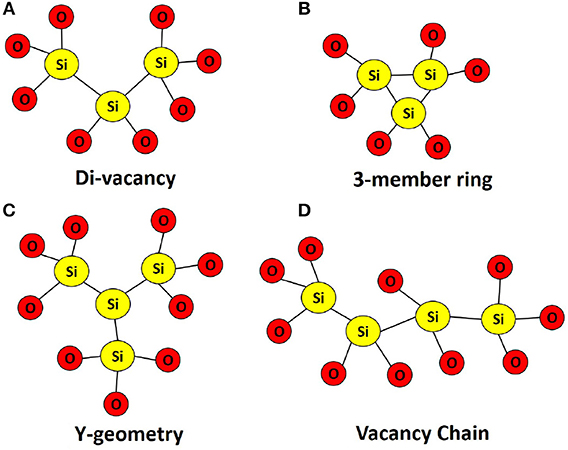
Figure 1. Typical geometries of (A) Oxygen di-vacancy in a-SiO2, (B–D) Oxygen tri-vacancies in a-SiO2. Oxygen tri-vacancies can occur in one of three configurations: a 3-member Ring; a “Y-geometry”; and as a vacancy chain.
In all cases considered, occupied states are observed within the band gap. For the di-vacancy case, a single state is observed between 1.27 and 1.97 eV above the VBM with a mean of 1.52 eV. For the tri-vacancy case, two states are observed at 0.35 to 2.04 eV and 1.40 to 2.47 eV above the VBM, with mean values of 1.23 and 1.97 eV, respectively. These states result from the pairing up of electrons from the remaining Si atoms when an oxygen atom is removed. The LUMO is positioned 5.64 to 7.68 eV and 6.10 to 6.92 eV above the VBM for di- and tri-vacancies, with mean values of 6.86 and 6.54 eV, respectively. Figure 2 illustrates how the LUMO state consists of an electron localized around a cluster site, with the shape of the orbital being dependent on the cluster geometry. In the di-vacancy and 3-member ring tri-vacancy cases (Figures 2A,B), the orbital lobes are situated above and below the plane of three Si atoms. This is different for the “Y” geometry and vacancy chain cases (Figures 2C,D), where orbital lobes are shared between the four Si atoms making up the vacancy. Typical density of states plots are shown in Figure 3 for a monovacancy and its corresponding di-vacancy and tri-vacancy. The formation of these states on average ever deeper in the band gap suggests that larger clusters may facilitate conduction processes such as trap-assisted tunneling.
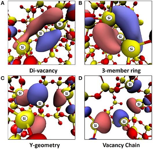
Figure 2. Typical LUMOs from (A) Oxygen di-vacancy in a-SiO2, (B) 3-member ring type tri-vacancy in a-SiO2, (C) Y-geometry type tri-vacancy in a-SiO2, (D) Vacancy chain type tri-vacancy in a-SiO2. Positive and negative iso-surfaces are shown in blue and red with iso values of ±0.05, respectively. The Si atoms belonging to each vacancy cluster are labeled.
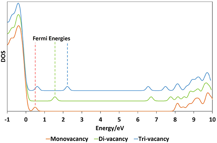
Figure 3. Example density of states plots for a monovacancy together with its corresponding di-vacancy and tri-vacancy. For clarity, the energy levels on the plot have been broadened using Gaussians with a FWHM of 0.1 eV. The dotted lines indicate the position of the Fermi energy for each configuration.
To study the interaction between vacancies in a-HfO2 we performed calculations for 15 different vacancy configurations. To produce di-vacancy models we take a subset of 9 single vacancies, and for each vacancy in this subset produce 3 di-vacancies by removing adjacent oxygen atoms. This produces 27 di-vacancy models in total. The choice of the original set of parent vacancies reflected the distribution of coordination numbers of oxygen atoms in our a-HfO2 models. In this approach, the second vacancy probes the local environment around the preexisting vacancy. Vacancy dimers can form as a result of vacancy diffusion, which is inefficient for neutral vacancies, or as a result of formation of new vacancies as a result of electron trapping by pre-existing vacancies discussed below. Efficiency of these processes is governed by energy barriers.
The interaction between neutral vacancies in a di-vacancy can be quantified by comparing the energy required to produce the first vacancy and then the second vacancy nearby. The first formation energy is calculated using Eq. 1. The second formation energy, , is calculated using EVac in place of EBulk, that is . If is lower than EF, the vacancies are said to be “attractive,” If , the vacancies are said to be “repulsive.” We note that the notion of “attractive,” and “repulsive” is blurred in amorphous structures as defect formation energy strongly depends on the local environment. We have checked that all geometric configurations of vacancy dimers are fully converged and hence variations in second vacancy formation energy are caused by the difference in the local environment of each site as well as by the overlap of the vacancy wavefunctions forming bonding states (see Figure 4). We have also carried out “reversibility" tests where the O atom is placed back into the vacancy and the geometry is optimized again. In all cases the system returns to the original geometry and total energy, indicating that the formation of the second vacancy does not cause topological changes of the local environment.
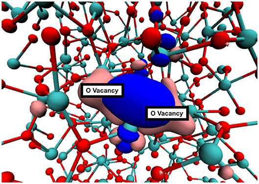
Figure 4. A typical oxygen di-vacancy in a-HfO2. The pink and blue surfaces show the |ψ|2 of the defects states. In this configuration, the vacancy states combine and look similar to bonding and antibonding orbitals.
The standard deviation of vacancy formation energies for our set of vacancies is 0.2 eV. Therefore we investigate the shift of the formation energy distribution by comparing average formation energies. On average, the second vacancy formation energy is 0.1 eV lower than that of the first. The standard deviation, however, is 0.4 eV. This means that some di-vacancy configurations will be of the “repulsive” type, even though the average case is “attractive.” A typical di-vacancy configuration in a-HfO2 is shown in Figure 4. Interaction between the vacancies is visualized by the plot of the di-vacancy doubly occupied electron states. Instead of two localized states adjacent to one another, the plot shows two states which are extended across the vacancies in a bond-like fashion. This type of molecular bonding type configuration corresponds to the majority of cases (approximately 80 %).
Further stabilization is possible for tri-vacancy clusters. The interaction in tri-vacancies can be quantified in a similar manner to di-vacancies by comparing the third vacancy formation energy with that of the second. It is found that the third vacancy formation energy is, on average, 0.2 eV lower than the second. Oxygen tri-vacancies have two general configurations, they can be organized in a linear or triangular fashion (see Figure 5). Similar to a-SiO2, the interaction between vacancies in a more compact triangular configurations is stronger-the formation energy of triangular clusters is, on average, 0.2 eV lower than that of linear clusters. The standard deviation of the tri-vacancy formation energy distribution is 0.5 eV. This means that, similar to the di-vacancy case, there exists tri-vacancy aggregates that are of the repulsive type, despite the fact that, on average, tri-vacancies are attractive.
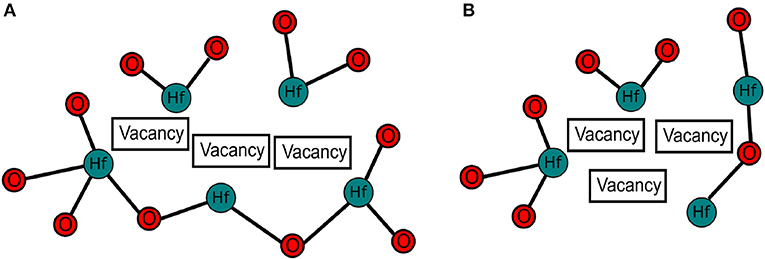
Figure 5. Schematic of the two types of oxygen tri-vacancy in a-HfO2. (A) shows the the linear type of configuration. (B) shows the triangular type of configuration. On average, triangular type tri-vacancies are lower in energy.
Therefore, the vacancy aggregation mechanism is the one in which the presence of a vacancy (or vacancies) lowers the formation energy required to produce an adjacent vacancy. This increases the rate of multi-vacancy generation relative to isolated vacancy generation.
In many applications, amorphous SiO2 and HfO2 films are sandwiched between electrodes with often strong (of the order of 1V/nm) electric field applied across them. Under such conditions, extra electrons can tunnel into the oxide conduction band or into defect states inside the oxide by TAT. These effects are known to cause degradation of performance of oxide layers as dielectric in devices [1, 4]. In particular, it has recently been suggested that electrons injected into a-SiO2 can be trapped in the amorphous matrix at structural precursor sites and form deep electron states in the band gap [44]. These intrinsic trapping sites have been identified as wide O–Si–O angles (>132°) in the continuous random network structure and can accommodate up to two electrons (see Figure 6). The formation of these bi-electron states lowers the energy barrier to create a neutral O-vacancy in a-SiO2 from about 8 eV to an average of 0.7 eV [45]. As a result of this process, an interstitial O2− ion is created in the amorphous network, as shown in Figures 6A–C. The concentration of precursor sites for intrinsic electron traps in a-SiO2 has been estimated at 4 × 10¹⁹ [44]. More information on the structure of electron traps, their optical absorption, EPR signatures, and a detailed description of electron injection facilitated Frenkel defect creation in a-SiO2 can be found in prior publications [44, 45].
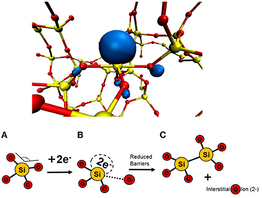
Figure 6. Schematic illustrating how trapping of two electrons at a precursor site facilitates creation of neutral O vacancy and interstitial O2− ion [45]. (A) Wide angle intrinsic traps in the amorphous network can trap two electrons. (B) Trapped electrons on the precursor reduce the barrier for O interstitial to be displaced. (C) O2− ion is displaced to create a vacancy-ion pair.
We note that neutral O-vacancies and negatively charged O2− interstitial ions created by this mechanism have an average recombination barrier of 0.8 eV [45]. The formation energy diagram for O vacancies in a-SiO2 is shown in Figure 7. The structural disorder of the amorphous material results in a wide range of local structures and hence a wide range of formation energy values. The charge transition levels of these vacancies exhibit a similar spread with an average 0/–1 charge transition level of 6.9 eV and an average –1/–2 charge transition level of 7.0 eV. Our results indicate that the charge transition levels which correspond to negatively charged vacancies are well positioned in relation to the conduction band of Si [46] and Fermi level position of some metal electrodes [47]. Thus, the newly created O vacancies can support trap assisted electron tunneling through a-SiO2 in Si/SiO2/metal stacks. The O2− ions can diffuse away through the oxide via a previously studied pivot mechanism [45] which is characterized by a low 0.3 eV energy barrier. Under some conditions, oxygen has been observed to release into the gas phase [11].
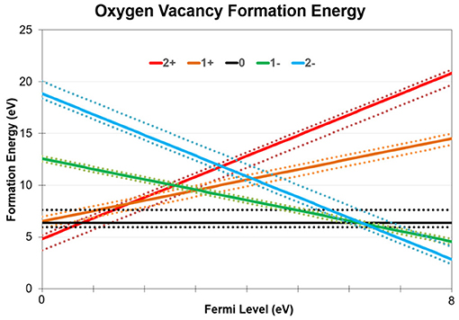
Figure 7. O vacancy formation energies in a-SiO2 at various charge states as a function of Fermi level. 144 vacancy geometries were calculated for each charge state due to the amorphous nature of our material. The average formation energy of each charge state is plotted using solid lines, while the minimum and maximum values for each charge state is plotted using dotted lines. The crossing point between positive and neutral vacancies is shown to be between 0.5 and 1.0 eV while the crossing point between neutral and negatively charged vacancies is between to be 6.2–7.5 eV.
A qualitatively similar mechanism for the formation of pairs of neutral O-vacancies and interstitial O2− ions in monoclinic and amorphous HfO2 has been proposed in Bradley et al. [48] and Kaviani et al. [49]. Extra electrons injected into monoclinic (m)-HfO2 can form relatively shallow polaron and bi-polarons with trapping energies of about 0.3 eV [50]. Simulations [48] demonstrate that the formation of stable pairs of neutral oxygen vacancies and interstitial oxygen ions assisted by extra electrons is thermodynamically feasible and requires overcoming activation barriers of about 2.0 eV. This barrier is reduced to <1.3 eV if two extra electrons are initially trapped at a pre-existing O-vacancy. This results in the formation of another O-vacancy nearby and a mobile interstitial O2− ion. The created O di-vacancy is stabilized by weak attraction between neutral vacancies, as described above. This leads to further lowering of the formation energy of the defect pair. The binding energy per vacancy in larger oxygen-vacancy aggregates increases as the aggregate grows, facilitating the formation of defect pairs next to larger vacancy aggregates.
In amorphous HfO2, extra electrons injected from an electrode form deep polaron and bi-polaron states [23]. Extra electrons localize in energetically deep states at intrinsic structural traps in a-HfO2 such as under-coordinated Hf ions or Hf ions with elongated Hf-O bonds, both of which are associated with a lowering of the electrostatic potential for an electron. The estimated density of such sites [23] in a-HfO2 is about 2 × 1021 cm−3. The structure and spectroscopic properties of these electron traps are described in detail in Kaviani et al. [23] and Strand et al. [51]. The bi-polaron formation causes strong Hf-O bond weakening manifested in significant (about 0.8 Å) ionic displacements. Similar to a-SiO2, thermal activation of these bi-polarons may cause the formation of Frenkel defects in a-HfO2 [49].
How electron trapping at pre-existing O-vacancies could facilitate the formation of new O-vacancies in a-SiO2 is discussed below.
As discussed above, O-vacancies in amorphous SiO2 and HfO2 create deep states in the band gap where electrons can tunnel from Si and other electrodes. One of the possible mechanisms of O-vacancy aggregation is via creation of new vacancies near the pre-existing ones. Below we consider whether this process can be facilitated by electron trapping by O-vacancies in a-SiO2. The cost of creating an oxygen vacancy depends greatly on the local environment. Not only is there a spread of formation energies owing to the disorder, but pre-existing vacancies can affect both the position and the barrier for forming a new vacancy. The presence of an existing vacancy close to the bi-polaron may either facilitate or hinder the next vacancy-creation process.
This can be manifested in several ways: (i) Electron trapping in a vacancy can facilitate the formation of a new vacancy nearby. (ii) Distortion of the surrounding network caused by electron trapping in a vacancy can create another precursor site for electron trapping nearby. Further electron trapping at these precursor sites can facilitate the creation of new vacancies. (iii) Aggregation of several vacancies can distort the surrounding network and enhance local electric field under electrical stress, facilitating creation of new vacancies. Below we consider mechanisms of some of these processes on the example of a-SiO2.
In a-SiO2, an O-vacancy can trap up to two electrons [52]. When two electrons localize onto an O-vacancy, the defect distorts as the two 3-coordinated Si atoms displace to point away from each other, as shown in Figure 8. As a result of this distortion, there is a small chance that one of the lobes of the HOMO localized on Si atoms of the vacancy will point directly at a neighboring 4-coordinated Si atom, facilitating the Si-Si bond formation by expelling an O atom. The HOMO of a negatively charged O vacancy is shown in Figure 8.
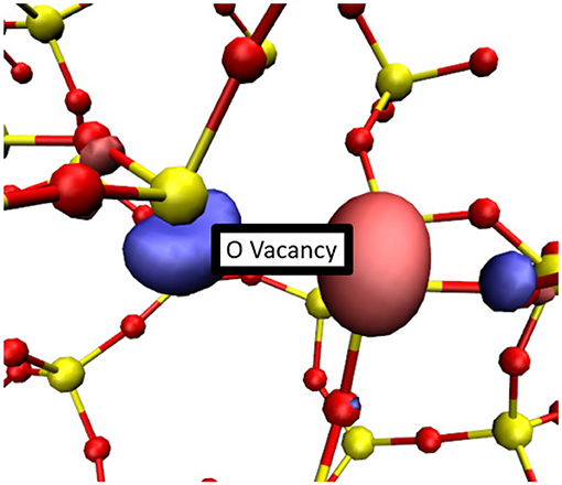
Figure 8. A typical configuration of a doubly-charged O-vacancy in a-SiO2. Two electrons have been trapped at this vacancy and the Si atoms within the vacancy pivot to point away from each other. Si atoms are shown in yellow while O atoms are shown in red. An iso-surface of the HOMO is shown in blue and pink.
To determine the likelihood of creating another O vacancy near an existing one, 144 possible vacancy geometries were investigated. In 97% of these geometries, the vacancy simply trapped two electrons by distorting, as shown in Figures 8, 9B. In 2 cases the HOMO happened to point at a neighboring 4-coordinated Si atom, as shown schematically in Figure 9C. This configuration facilitates the creation of another O vacancy and O interstitial ion through a process with an average barrier of 1.1 eV. A schematic of formation of another vacancy correlated with the pre-existing vacancy is shown in Figures 9A–D. However, it is important to note that this process is relatively rare and was only observed in 2 out of 144 cases considered here.
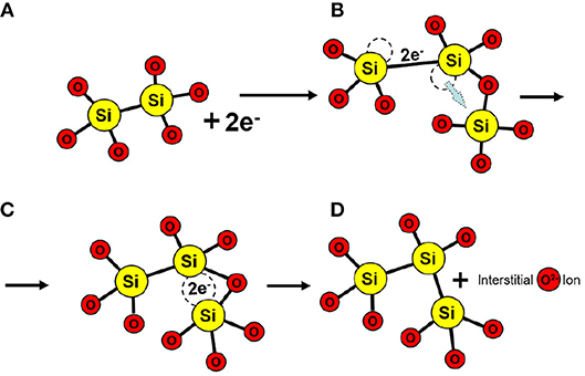
Figure 9. Schematic illustrating the correlated defect creation mechanism. (A) O Vacancies can trap up to two electrons; and (B) distort the amorphous structure. (C) In rare cases, the HOMO of the charged vacancy points toward a neighboring Si atom and forms a bond to (D) create a new vacancy and interstitial O.
Another possibility is that new wide O–Si–O angle precursor sites for electron trapping are created when O vacancies are occupied by electrons. Trapping two electrons at these new precursors can lead to creation of O vacancies by the mechanism illustrated in Figures 6A–C. The creation of these traps is directly related to the amount of local strain present in the system. Both the creation of new vacancies and the localization of electrons at existing vacancies result in an increase of local network distortion. After the geometry of each doubly negatively charged O vacancy was relaxed, another electron was added into the system to probe whether precursor sites for electron trapping were created. Out of a total of 142 geometries (excluding the two examples of correlated defect creation) a new wide O–Si–O angle intrinsic trapping site was found 38 times. In these cases new wide O–Si–O bond angle sites, which did not exist before, were created by the network distortion induced by the charged vacancy relaxation, as shown in Figure 10. Due to flexibility of a-SiO2 network, wide angle precursors created in this way are not necessarily at neighboring sites to the vacancy responsible for distorting the local geometry. The probability of creating these new precursor sites is about 25%. Trapping two electrons at these new precursor sites generates new O vacancies and interstitial O2− ions, as described above.
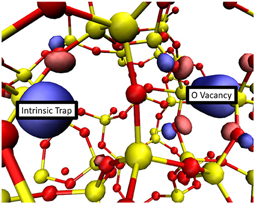
Figure 10. The HOMO of a doubly negative O vacancy and a strain-induced wide O-Si-O angle intrinsic electron trap. In about 25% of geometries the third electron injected into a system which already contains a doubly negatively charged O vacancy localized onto a newly created intrinsic trap. Si atoms are shown in yellow while O atoms are shown in red. An iso-surface of the HOMO is shown in blue and pink.
Since creation of additional wide O–Si–O angle intrinsic electron traps is associated with the local strain due to the presence of defects, one can expect that increasing the concentration of such defects should increase the probability of generating new precursor sites for electron trapping. As additional vacancies are created near pre-existing ones, the amount of local strain produced increases as well. To investigate this effect, we examined 40 di-vacancy geometries using 214 atom periodic cells. As electrons were added into these simulations, they can either localize in one vacancy, creating an equivalent of one negatively charged vacancy and one neutral vacancy or, if the di-vacancy exhibits a high degree of symmetry, they can be shared between the two, as shown in Figure 2. When up to 2 electrons are localized into the di-vacancy, creation of new precursor sites was observed 10 times, the same as for single vacancies. However, when the defect states are fully occupied by 4 electrons, it was observed that in 20 cases out of 40 wide O–Si–O bond angle sites were created due the network distortion caused by electron trapping at existing vacancies. This demonstrates that indeed clustering of O vacancies and electron trapping in them increase the probabilities of creating new vacancies nearby and these of growing new vacancy clusters.
We further investigated this trend by examining whether O tri-vacancies will also induce wide O–Si–O angle precursor sites. To accommodate such large vacancy clusters, we created a library of 648-atom a-SiO2 cells using the melt and quench procedure described above. These larger amorphous structures were then screened for existing defects or wide O–Si–O angle intrinsic traps and 5 defect-free geometries were selected. Using these large cells, three libraries of tri-vacancy geometries were created to account for the more variable structure of these larger clusters. The first set of tri-vacancy geometries consisted of examples where the three defects were tightly clustered. The second set was composed of examples where the three defects were arranged in a linear array. Finally, in the third set of geometries each contained three loosely associated vacancies within two nearest neighbor sites of each other. Ten geometries from each set were selected for analysis at random and each of them was simulated with 1–6 extra electrons in the system.
In 23 out of 30 geometries, strain-induced wide O–Si–O angle electron traps were observed after all the pre-existing vacancies were charged. These newly created intrinsic traps were evenly distributed between the three types of tri-vacancy geometries, indicating that their exact configuration does not have a large effect on the correlated creation of new defects. When the tri-vacancy structures were charged with up to 2 electrons a new intrinsic trap was observed in 8 cases and when they were charged with up to 4 electrons a new intrinsic trap was observed in 14 geometries.
These results suggest that, as the size of O vacancy clusters increases, the likelihood of creating another vacancy nearby increases as well. Single vacancies have a 25% chance of inducing a wide O-Si-O angle intrinsic electron trap when charged, di-vacancies have a 50% chance, and tri-vacancies are the most likely to create a nearby intrinsic trap with a 77% chance. It also indicates that a significant portion of the network distortion that is responsible for the newly formed traps can be attributed to the localization of injected electrons rather than the presence of the vacancy cluster itself.
The mechanism of creation of a second O-vacancy facilitated by an electron trapping at a pre-existing vacancy in m-HfO2 has been described in Bradley et al. [48]. The qualitative similarities in vacancy formation and aggregation processes in a-SiO2 and a-HfO2 suggest that such mechanisms can be operational also in a-HfO2. They will be discussed in a separate publication.
Understanding the mechanisms of aggregation of oxygen vacancies in dielectric oxides is important for improving their performance in electronics, sensors, catalysis and other applications under electrical stress and different types of irradiation. We reviewed the initial stages of O-vacancy clustering in two prototype wide bandgap oxides, SiO2 and HfO2, and demonstrated that this is energetically favorable in some vacancy configurations. However, barriers for neutral O-vacancy diffusion in both materials are high and their aggregation via thermally activated diffusion is unfeasible at room temperature. As an alternative mechanism of vacancy aggregation, we considered how new O-vacancies can be created as a result of electron trapping by pre-existing ones on the example of a-SiO2. These electrons can be injected via tunneling from an electrode in a device or produced under irradiation process. The results demonstrate that trapping two electrons at O vacancy sites in a-SiO2 induces local distortion in the amorphous network such that new O–Si–O precursor sites for electron trapping are created with a probability of about 25%. These sites can trap two extra electrons, producing a new vacancy nearby. As the size of the O vacancy clusters increases, the likelihood of creating another vacancy nearby increases as well. Di-vacancies have a 50% chance, and tri-vacancies are the most likely to create a nearby intrinsic trap with a 77% chance.
These results suggest that electron trapping at oxygen vacancies in amorphous and crystalline oxides may facilitate the creation of new vacancies and this process becomes more efficient as vacancy clusters grow larger because this requires less activation. Previous results suggest that a similar mechanism can be also operational in m-HfO2. We hope that these results will stimulate further studies of oxygen vacancy aggregation in other functional oxides, such as Al2O3 and Ga2O3 as well as in nitrides.
The datasets generated for this study are available on request to the corresponding author.
DG and MM have performed and analyzed calculations for oxygen vacancy aggregation in a-SiO2 and wrote the corresponding parts of the paper. JS has performed and analyzed calculations for oxygen vacancy aggregation in a-HfO2 and wrote the corresponding parts of the paper. AS coordinated the research, participated in analyzing the results and wrote and edited the paper.
We acknowledge funding provided by the UK Engineering and Physical Sciences Research Council (EPSRC) under grants No. EP/K01739X/1 and EP/P013503/1 and by the Leverhulme Trust RPG-2016-135. JS is funded by EPSRC grant no. EP/G036675/1 to the Center for Doctoral Training. Computer facilities on Archer service have been provided via the UKs HPC Materials Chemistry Consortium (EPSRC Grant No. EP/L000202).
The authors declare that the research was conducted in the absence of any commercial or financial relationships that could be construed as a potential conflict of interest.
The authors are grateful to L. Larcher, A. Padovani, and G. Bersuker for valuable and stimulating discussions. Part of the results presented in this paper were previously published in The 2018 IEEE Reliability Physics Symposium [53].
1. Fleetwood DM. Defects in Microelectronic Materials and Devices. Fleetwood DM, Pantelides ST, Schrimph RD, editors. Boca Raton, FL: CRC Press (2009).
2. Kuzum D, Yu S, Wong HSP. Synaptic electronics: materials, devices and applications. Nanotechnology. (2013) 24:382001. doi: 10.1088/0957-4484/24/38/382001
3. Mehonic A, Shluger AL, Gao D, Valov I, Miranda E, Ielmini D, et al. Silicon oxide (SiOx): a promising material for resistance switching? Adv Mater. (2018) 30:1801187. doi: 10.1002/adma.201801187
4. Grasser T. Bias Temperature Instability for Devices and Circuits. Grasser T editor. New York, NY: Springer Science & Business Media (2013).
5. McPherson J. Time dependent dielectric breakdown physics-Models revisited. Microelectron Reliab. (2012) 52:1753–60. doi: 10.1016/j.microrel.2012.06.007
6. Foster AS, Gejo FL, Shluger AL, Nieminen RM. Vacancy and interstitial defects in hafnia. Phys Rev B. (2002) 65:174117. doi: 10.1103/physrevb.65.174117
7. Gao DZ, Strand J, El-Sayed AM, Shluger AL. Role of electron and hole trapping in the degradation and breakdown of SiO2 and HfO2 films. In: 2018 IEEE International Reliability Physics Symposium (IRPS). (2018). p. 5A.2–1–5A.2–7.
8. Degreave R, Kaczer B, Groeseneken G. Degradation and breakdown in thin oxide layers: mechanisms, models and reliability prediction. Microelectron. Reliab. (1999) 39:1445–60.
9. Green ML, Gusev EP, Degraeve R, Garfunkel EL. Ultrathin (< 4 nm) SiO2 and Si–O–N gate dielectric layers for silicon microelectronics: understanding the processing, structure, and physical and electrical limits. J Appl Phys. (2001) 90:2057–121. doi: 10.1063/1.1385803
10. Padovani A, Gao DZ, Shluger AL, Larcher L. A microscopic mechanism of dielectric breakdown in SiO2 films: An insight from multi-scale modeling. J Appl Phys. (2017) 121:155101. doi: 10.1063/1.4979915
11. Mehonic A, Buckwell M, Montesi L, Munde MS, Gao DZ, Hudziak S, et al. Nanoscale transformations in metastable, amorphous, silicon Rich silica. Adv Mater. (2016) 28:7486–93. doi: 10.1002/adma.201601208
12. Ambrogio S, Magyari-Kope B, Onofrio N, Islam MM, Duncan D, Nishi Y, et al. Modeling resistive switching materials and devices across scales. J Electroceram. (2017) 39:39–60. doi: 10.1007/s10832-017-0093-y
13. Setvin M, Schmid M, Diebold U. Aggregation and electronically induced migration of oxygen vacancies in TiO2 anatase. Phys Rev B. (2015) 91:195403. doi: 10.1103/PhysRevB.91.195403
14. Magyari-Kope B, Tendulkar M, Park SG, Lee HD, Nishi Y. Resistive switching mechanisms in random access memory devices incorporating transition metal oxides: TiO2, NiO and Pr0.7Ca0.3MnO3. Nanotechnology. (2011) 22:254029. doi: 10.1088/0957-4484/22/25/254029
15. Esch F, Fabris S, Zhou L, Montini T, Africh C, Fornasiero P, et al. Electron Localization Determines Defect Formation on Ceria Substrates. Science. (2005) 309:752–5. doi: 10.1126/science.1111568
16. Wang L, Yu Y, He H, Zhang Y, Qin X, Wang B. Oxygen vacancy clusters essential for the catalytic activity of CeO2 nanocubes for o-xylene oxidation. Sci Rep. (2017) 7:12845. doi: 10.1038/s41598-017-13178-6
17. Eom K, Choi E, Choi M, Han S, Zhou H, Lee J. Oxygen vacancy linear clustering in a perovskite oxide. J Phys Chem Lett. (2017) 8:3500–5. doi: 10.1021/acs.jpclett.7b01348
18. Henderson B, Wertz JE. Defects in the alkaline earth oxides. Defects in the alkaline earth oxides. Adv Phys. (1968) 17:749–855. doi: 10.1080/00018736800101386
19. Munde MS, Gao DZ, Shluger AL. Diffusion and aggregation of oxygen vacancies in amorphous silica. J Phys. (2017) 29:245701. doi: 10.1088/1361-648X/aa6f9a
20. Bradley S, Bersuker G, Shluger A. Modelling of oxygen vacancy aggregates in monoclinic HfO2: can they contribute to conductive filament formation? J Phys. (2015) 27:415401. doi: 10.1088/0953-8984/27/41/415401
21. Capron N, Broqvist P, Pasquarello A. Migration of oxygen vacancy in HfO2 and across the HfO2/SiO2 interface: a first principles investigation. Appl Phys Lett. (2007) 91:192905. doi: 10.1063/1.2807282
22. El-Sayed AM, Watkins MB, Afanas'ev VV, Shluger AL. Nature of intrinsic and extrinsic electron trapping in SiO2. Phys Rev B. (2014) 89:125201. doi: 10.1103/PhysRevB.89.125201
23. Kaviani M, Strand J, Afanas'ev VV, Shluger AL. Deep electron and hole polarons and bipolarons in amorphous oxide. Phys Rev B. (2016) 94:020103. doi: 10.1103/PhysRevB.94.020103
24. van Duin ACT, Strachan A, Stewman S, Zhang Q, Xu X, Goddard W. ReaxFFSiO reactive force field for silicon and silicon oxide systems. J Phys Chem A. (2003) 107:3803. doi: 10.1021/jp0276303
25. Fogarty JC, Aktulga HM, Grama AY, van Duin ACT, Pandit SA. J Chem Phys. (2010) 132:174704. doi: 10.1063/1.3407433
26. Plimpton S. Fast parallel algorithms for short-range molecular dynamics. J Comp Phys. (1995) 117:1. doi: 10.1006/jcph.1995.1039
27. Yu Y, Wang B, Wang M, Sant G, Bauchy M. Revisiting silica with ReaxFF: towards improved predictions of glass structure and properties via reactive molecular dynamics. J Non-Cryst Solids. (2016) 443:148–54. doi: 10.1016/j.jnoncrysol.2016.03.026
28. Broglia G, Ori G, Larcher L, Montorsi M. Molecular dynamics simulation of amorphous HfO2 for resistive RAM applications. Model Simul Mater Sci Eng. (2014) 22:065006. doi: 10.1088/0965-0393/22/6/065006
29. Lippert G, Hutter J, Parrinello M. A hybrid Gaussian and plane wave density functional scheme. Mol Phys. (1997) 92:477–87. doi: 10.1080/002689797170220
30. VandeVondele J, Krack M, Mohamed F, Parrinelo M, Chassaing T, Hutter J. Quickstep: fast and accurate density functional calculations using a mixed Gaussian and plane waves approach. Comput Phys Commun. (2005) 167:103. doi: 10.1016/j.cpc.2004.12.014
31. Guidon M, Hutter J, VandeVondele J. Robust periodic Hartree-Fock exchange for large-scale simulations using Gaussian basis sets. J Chem Theory Comput. (2009) 5:3013. doi: 10.1021/ct900494g
32. Guidon M, Hutter J, VandeVondele J. Auxiliary density matrix methods for hartreefock exchange calculations. J Chem Theory Comput. (2010) 8:2348. doi: 10.1021/ct1002225
33. VandeVondele J, Hutter J. Gaussian basis sets for accurate calculations on molecular systems in gas and condensed phases. J Chem Phys. (2007) 127:114105. doi: 10.1063/1.2770708
34. Goedecker S, Teter M, Hutter J. Separable dual-space Gaussian pseudopotentials. Phys Rev B. (1996) 54:1703. doi: 10.1103/PhysRevB.54.1703
35. Vollmayr K, Kob W, Binder K. Cooling-rate effects in amorphous silica: a computer-simulation study. Phys Rev B. (1996) 54:15808. doi: 10.1103/PhysRevB.54.15808
36. Susman S, Volin KJ, Price DL, Grimsditch M, Ringo JP, Kalia RK, et al. Intermediate-range order in permanently densified vitreous SiO2: a neutron-diffraction and molecular-dynamics study. Phys Rev B. (1991) 43:1194. doi: 10.1103/PhysRevB.43.1194
37. Lany S, Zunger A. Accurate prediction of defect properties in density functional supercell calculations. Model Simul Mater Sci Eng. (2009) 17:084002. doi: 10.1088/0965-0393/17/8/084002
38. Murphy ST, Hine NDM. Anisotropic charge screening and supercell size convergence of defect formation energies. Phys Rev B. (2013) 87:094111. doi: 10.1103/PhysRevB.87.094111
40. El-Sayed AM. Atomistic Modelling of Charge Trapping Defects in Silicon Dioxide. London: University College London (2015).
41. Martin-Samos L, Limoge Y, Richards N, Crocombette JP, Roma G, Anglada E, et al. Oxygen neutral defects in silica: Origin of the distribution of the formation energies. Europhys Lett. (2004) 66:680. doi: 10.1209/epl/i2003-10247-3
42. Mukhopadhyay S, Sushko P, Stoneham AM, Shluger AL. Modeling of the structure and properties of oxygen vacancies in amorphous silica. Phys Rev B. (2004) 19:195203. doi: 10.1103/PhysRevB.70.195203
43. Sushko P, Mukhopadhyay S, Stoneham AM, Shluger AL. Oxygen vacancies in amorphous silica: structure and distribution of properties. Microelectron Eng. (2005) 80:292–5. doi: 10.1016/j.mee.2005.04.083
44. El-Sayed AM, Watkins MB, Shluger AL, Afanas'ev VV. Identification of intrinsic electron trapping sites in bulk amorphous silica from ab initio calculations. Microelectron Eng. (2013) 109:68–71. doi: 10.1016/j.mee.2013.03.027
45. Gao DZ, El-Sayed AM, Shluger AL. A mechanism for Frenkel defect creation in amorphous SiO2 facilitated by electron injection. Nanotechnology. (2016) 27:505207. doi: 10.1088/0957-4484/27/50/505207
46. Afanas'ev V, Kolomiiets N, Houssa M, Stesmans A. Internal photoemission metrology of inhomogeneous interface barriers. Phys Stat Solidi A. (2017) 215:1700865. doi: 10.1002/pssa.201700865
47. Yeo YC, King TJ, Hu C. Metal-dielectric band alignment and its implications for metal gate complementary metal-oxide-semiconductor technology. J Appl Phys. (2002) 92:7266–71. doi: 10.1063/1.1521517
48. Bradley SR, Shluger AL, Bersuker G. Electron-injection-assisted generation of oxygen vacancies in monoclinic HfO2. Phys Rev Appl. (2015) 4:064008. doi: 10.1103/PhysRevApplied.4.064008
49. Strand J, Kaviani M, Shluger AL. Defect creation in amorphous HfO2 facilitated by hole and electron injection. Microel Eng. (2017) 178:279–83. doi: 10.1016/j.mee.2017.05.005
50. Ramo DM, Shluger A, Gavartin J, Bersuker G. Theoretical prediction of intrinsic self-trapping of electrons and holes in monoclinic HfO2. Phys Rev Lett. (2007) 99:155504. doi: 10.1103/PhysRevLett.99.155504
51. Strand J, Kaviani M, Afanas'ev VV, Lisoni JG, Shluger AL. Intrinsic Electron Trapping in Amorphous Oxides. Nanotech. (2018) 29:125703. doi: 10.1088/1361-6528/aaa77a
52. Kimmel AV, Sushko PV, Shluger AL, Bersuker G. A microscopic mechanism of dielectric breakdown in SiO2 films: An insight from multiscale modelling. Electrochem Soc Trans. (2009) 19:3–17. doi: 10.1063/1.4979915
Keywords: dielectric oxides, oxygen vacancies, Density Functional Theory, SiO2, HfO2
Citation: Gao DZ, Strand J, Munde MS and Shluger AL (2019) Mechanisms of Oxygen Vacancy Aggregation in SiO2 and HfO2. Front. Phys. 7:43. doi: 10.3389/fphy.2019.00043
Received: 16 November 2018; Accepted: 07 March 2019;
Published: 29 March 2019.
Edited by:
Maria Veronica Ganduglia-Pirovano, Instituto de Catálisis y Petroleoqumica (ICP), SpainReviewed by:
Cesare Franchini, University of Vienna, AustriaCopyright © 2019 Gao, Strand, Munde and Shluger. This is an open-access article distributed under the terms of the Creative Commons Attribution License (CC BY). The use, distribution or reproduction in other forums is permitted, provided the original author(s) and the copyright owner(s) are credited and that the original publication in this journal is cited, in accordance with accepted academic practice. No use, distribution or reproduction is permitted which does not comply with these terms.
*Correspondence: Jack Strand, amFjay5zdHJhbmQuMTRAdWNsLmFjLnVr
Disclaimer: All claims expressed in this article are solely those of the authors and do not necessarily represent those of their affiliated organizations, or those of the publisher, the editors and the reviewers. Any product that may be evaluated in this article or claim that may be made by its manufacturer is not guaranteed or endorsed by the publisher.
Research integrity at Frontiers
Learn more about the work of our research integrity team to safeguard the quality of each article we publish.