95% of researchers rate our articles as excellent or good
Learn more about the work of our research integrity team to safeguard the quality of each article we publish.
Find out more
ORIGINAL RESEARCH article
Front. Phys. , 20 September 2018
Sec. Optics and Photonics
Volume 6 - 2018 | https://doi.org/10.3389/fphy.2018.00099
This article is part of the Research Topic Perovskite Solar Cells towards High Performance and High Stability View all 4 articles
Bathocuproine (BCP) was first employed as the interface buffer layers between the PCBM and Ag layers to improve the performance of Cs0.08(MA0.17FA0.83)0.92Pb(I0.83Br0.17)3 perovskite solar cells based on NiOx hole transporting layers. The effect of different evaporation times on the performance of solar cells at the same evaporation temperature (100°C) was carefully investigated. The optimum device efficiency of 14.47% was obtained by evaporating BCP for 36 s, suggesting an enhancement of 14% as compared to the cell without BCP modification.
Energy has always been an important impetus for the development of human civilization. In recent years, the adverse effects of the energy crisis have become more and more prominent. Solar cells have been widely recognized as the most effective way to directly convert solar energy into electricity, and a promising renewable energy technology that can support sustainable human development [1]. Inorganic-organic hybrid perovskite solar cells (PSCs) are expected to become a new generation of high-performance thin-film solar cells owing to their excellent absorption and charge transfer performance. Since 2009, the inorganic-organic hybrid perovskite solar cells have developed rapidly and the highest efficiency has reached 22.1% [2], which is comparable to the silicon-based solar cells. The most efficient device is the mesoporous n-i-p structured PSCs, usually using TiO2 and spiro-OMeTAD as the electron transporting layer (ETL) and hole transporting layer (HTL), respectively. Although the mesoporous structure can obtain high photoelectric conversion efficiency, it is necessary to use high-temperature annealing to prepare mesoporous TiO2 layers, thereby limiting the rapid and efficient manufacturing in the industry [3]. Compared with the mesoporous structured PSCs, the planar heterogeneous structure is simpler and more flexible, and the preparation process of the cells is relatively simple, which provides the possibility for the large-scale commercial production under low temperature conditions. Therefore, more and more attention is paid to optimizing the charge transport and perovskite layers in the planar p-i-n structure to improve the device performance [4–6]. In order to realize the commercial production of PSCs, it requires not only high photoelectric conversion efficiency, but also good stability of the device via a low-temperature fabrication route. Recently, Saliba et al. introduced a triple cation Csx(MA0.17FA0.83)(100–x)Pb(I0.83Br0.17)3 perovskite in the n-i-p structure, reaching PCE values of more than 20% together with good light stability and perovskite crystallinity compared with the traditional perovskite system [7]. In addition, metal compounds, such as CuOx [8], CuS [9], CuSCN [10], NiO [11, 12], and GeO [13] have been suggested as inorganic hole transport materials to replace PEDOT:PSS due to its expensiveness in commercial production and poor mechanical stability in flexible devices [14]. Therefore, the combination of the triple cation perovskite and the inorganic charge transfer materials can meet the commercial production conditions for PSCs. Recently, Stefan Weber et al. used NiO as HTL in a triple cation perovskite planar heterojunction solar cell, but its efficiency was only up to 12.8% [15].
In this regard, in order to realize the preparation of high-efficiency and high-stability planar triple cation perovskite solar cells, the effect of bathocuproine (BCP) as an interface buffer layer on the performance of the device was studied. In this work, the planar PSCs with an ITO/NiO/perovskite/PCBM/BCP/Ag structure were prepared, where BCP was obtained by thermal evaporation. After several control experiments, the best BCP evaporation time of 36 s (thermal evaporation temperature: 100°C) was achieved, reaching a PCE value of 14.47% that increased by 14% compared to the cell without BCP.
NiOx nanocrystals (NCs) were synthesized based on previously reported literature with slight modification [16, 17]. First of all, Ni(NO3)2·6H2O (0.1 mol) was dispersed in 60 mL deionized water to obtain a dark green solution. Then, using a syringe pump to control the injection rate at 1 mL/h, a 40 mL KOH solution was slowly add into the above solution with stirring. The resultant colloidal precipitate was washed three times with deionized water and dried at 70°C over night. After that, the green powder was annealed at 270°C for 2 h to get a dark-black powder. The synthesized nanocrystals were dissolved in deionized water at a concentration of 15 mg/mL and sonicated to obtain a spin-coating precursor solution in which the NiOx NCs were uniformly dispersed.
The preparation method of triple cation perovskite was adopted from Neha Arora et al. [10]. First, CH(NH2)2I (FAI, 1.0 M), PbI2 (1.1 M), PbBr2 (0.2 M), and CH3NH3Br (MABr, 0.2 M) were dissolved in a solution of dimethylformamide (DMF) and dimethyl sulfoxide (DMSO) by volume ratio of 4:1, stirred for 1 h, and then a CsI solution (5% volume, 1.5 M DMSO) was added to the mixed solution and stirred for another 1 h to obtain a perovskite precursor solution. The above solution was spin-coated on the ITO substrates via the one-step method to prepare Cs0.08(MA0.17FA0.83)0.92Pb(I0.83Br0.17)3 perovskite films.
First, the ITO-coated glass substrates were ultrasonically washed in detergent, deionized water, acetone and ethanol for 20 min followed by 15 min of ultraviolet-ozone treatment. The NiOx NCs film was deposited by spin-coating the NiOx NCs precursor solution at 2,500 r for 30 s on the ITO glass and annealed at 150°C for 20 min in air. After that, perovskite film was obtained in a glove box using a one-step spin-coating the triple cation perovskite precursor solution followed by the deposition of a thick [6, 6]-Phenyl C61 butyric acid methyl ester (PCBM) layer as ETL. Finally, BCP and Ag layers were successively evaporated on the PCBM layer.
The morphologies of NiOx NCs and perovskite samples were observed by field-emission scanning electron microscopy (FESEM, 10 kV). The crystal structure was examined by X-ray Diffraction (XRD, Panalytical X'pert Pro) with a Cu Kα source. The photovoltaic J-V measurement was performed under a solar simulator (500 W Model 91160, Newport) with an AM 1.5 spectrum to simulate a full sun intensity (100 mW/cm2). The IPCE was elucidated by a specially designed IPCE system for solar cells by PV Measurements, Inc., USA. The calibration of the system was done using a NIST-calibrated a silicon photodiode G425 as the standard before every IPCE. The IPCE results of the PSCs were collected as a function of wavelength from 300 to 900 nm using a 75 W Xe lamp as a light source for generating monochromatic beam at a low chopping frequency. Electrochemical Impedance Spectroscopy (EIS) was recorded at 0.7V bias on a CHI660E electrochemical workstation under a frequency range from 100 kHz to 0.1 Hz. The equivalent circuit models were used to analyze the impedance spectra.
Figure 1A displays the X-ray diffraction (XRD) pattern of the NiOx NCs with the diffraction peaks at 2θ = 37.2, 43.3, 62.7, 75.4, and 79.4°, which match well with the cubic NiOx (PDF No. 01-078-0429). Then, the XRD pattern of the triple cation perovskite deposited on the ITO-coated glass substrates (Figure 1B) showed all characteristic diffraction peaks according to the literature [5].
The surface morphology of a NiOx film prepared on a glass/ITO substrate was investigated by SEM as shown in Figure 2A. A NiOx thin film with uniform particle size completely covered on the substrate surface. Perovskite films with low crystal defects and good crystallinity were deposited on NiOx HTL by the one-step method as shown in Figure 2B. Figure 2C is a cross-sectional SEM image of a perovskite solar cell showing the deposition of each layer of the device.

Figure 2. SEM images of the (A) NiOx NCs, (B) the perovskite, and (C) the cross sectional SEM image of the inverted planar perovskite solar cell.
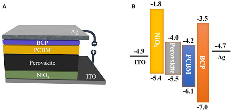
The triple cation Cs0.08(MA0.17FA0.83)0.92Pb(I0.83Br0.17)3 perovskite solar cells were fabricated using BCP as a buffer layer. For comparison, a PSC device was fabricated without BCP layer. Figure 3A shows the architecture of the fabricated device. We used a planar heterogeneous structure to assemble the PSCs. Compared with the mesoporous structured PSCs, the planar heterogeneous structure was prepared with relatively simple preparation process. Energy level diagram for each layer of the device are depicted in Figure 3B, in which the energy levels are obtained from the published works [18, 19].

Figure 3. Schematic diagrams of (A) The device structure of ITO/NiOx/Perovskite/PCBM/BCP/Ag; and (B) the band energy diagrams for the inverted structured perovskite solar cell.
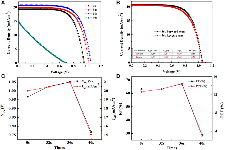
Four groups of controlled experiments were set up by controlling the thermal evaporation time: 0, 32, 36, and 40 s, respectively. Their scan J-V curves under simulated solar light are shown in Figure 4A. In addition, the detailed photovoltaic parameters of the J-V curves are summarized in Table 1. From the J-V curves, it could be seen that the thermal evaporation time of BCP significantly affected the performance of PSCs. As the evaporation time increased, the power conversion efficiency (PCE), short-circuit current density (JSC), open-circuit voltage (VOC), and fill factor (FF) of the PSCs increased first and then decreased (Figures 4C,D). When the evaporation time is 36 s, the photovoltaic parameters of PSCs were optimum: PCE = 14.47%, JSC = 21 mA/cm2, VOC = 1.051 V, and FF = 67%, the J-V curve of which is shown in Figure 4B. It is known that the FF and JSC values are closely related to the series and parallel resistance of the device. Therefore, with the prolonging of the evaporation time, the device performance changes may be due to the changes in series and shunt resistances.

Figure 4. (A) J-V curves under the AM 1.5 G simulated sunlight illumination (100 mW/cm2) for the inverted planar perovskite solar cells with different BCP evaporation times; (B) J-V curves of the best performance of the PSCs with BCP evaporation time 36 s; Changes of the (C) open-circuit voltage (VOC) and short-circuit photocurrent density (JSC), (D) fill factor (FF) and power conversion efficiency (PCE) at different BCP evaporation times.

Table 1. The photovoltaic parameters of the perovskite solar cells with varying BCP evaporation times.
There are different contact mechanisms between metal and semiconductor [20]. Introducing the BCP as the buffer layer between the PCBM and Ag layers was mainly to change the contact mode between the electron transport layer and the metal layer. When there was no steaming-plating BCP, the PCBM layer of the device was directly contacted with the Ag layer. The difference in Fermi energy levels created a built-in field, resulting in the band of semiconductors at the interface being bent to form the Schottky barrier. The presence of a barrier resulted in a large interface resistance and caused charge accumulation at the interface, so the device performance was somewhat poor. When the evaporation time was between 0 and 36 s, the thickness of BCP slowly increased, which intervened between the PCBM and Ag layers to hinder their mutual contact, and then made the original Schottky barrier lower with reduced interfacial resistance. Finally, the interface contact mechanism was changed from Schottky contact to Ohmic contact. As shown in Figure 4A, the performance of the batteries gradually increased and reached the championship level in the evaporation time of 36 s when a good Ohmic contact was established among the PCBM/BCP/Ag layers. However, with the continuous deposition of BCP after 40 s, the migration distance of electrons from the PCBM layer to the Ag layer became longer, increasing the recombination of the carriers and leading to the sharp drop of the device performance.
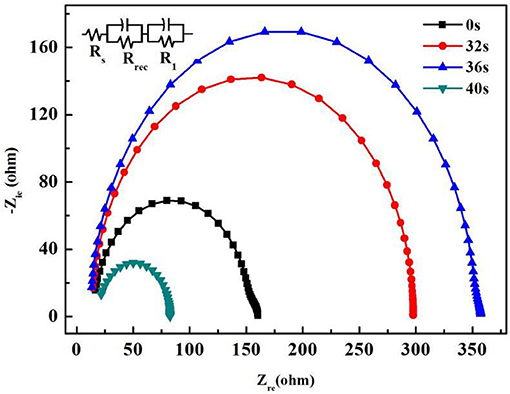
Furthermore, Figure 5 shows the electrochemical impedance spectra (EIS) of PSCs with different evaporation times (The inset shows the equivalent electronic circuit used to fit the experimental data). RS represents the series resistance of the device. R1 is the resistance related to diffusion of holes through the hole transporting material (HTM) with capacitance. The recombination resistance Rrec is associated with the interface of the perovskite and PCBM/BCP/Ag layers, which is inversely proportional to the recombination rate [21]. From Figure 5 and Table 2, it can be seen that when the evaporation time of BCP is 0 s, the perovskite solar cell has the largest series resistance RS and the smallest recombination resistance Rrec. With the increase of evaporation time, the series resistance (RS) of the device gradually decreases and the recombination resistance (Rrec) gradually increases. This shows that the contact mechanism between PCBM and Ag is changed from the Schottky contact to the ohmic contact. In addition, the minimum series resistance (RS) and the maximum composite resistance (Rrec) are achieved at the PCBM/BCP (36 s)/Ag interface. In other words, when the evaporation time is 36 s, the device performance is also optimal, as shown in Table 1. However, with the continuous deposition of BCP after 40 s, the migration distance of electrons from the PCBM layer to the Ag layer became longer, leading to increased series resistance (RS) and reduced recombination resistance (Rrec) and resulting in the sharp drop of the device performance. In other words, vapor-depositing the BCP layer in the devices improved the interfacial contact between the PCBM and Ag layers, thereby allowing the cell to possess low recombination rate [22]. This exactly coincides with the test results of the above J-V curves and the analysis of the effect mechanism of BCP.

Figure 5. Nyquist plots of the PCBM/Ag and PCBM/BCP/Ag based PSCs at 0.7 V bias under dark (The inset shows the equivalent electronic circuit used to fit the experimental data).

Table 2. The series resistances RSand the recombination resistance Rrecvalues of the perovskite solar cells with varying BCP evaporation times.
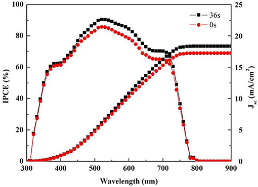
The performance of the PSCs was further investigated in terms of the IPCE efficiency to explain the light harvesting, charge collection, and photocurrent in devices. Figure 6 shows the IPCE plots of the PSCs with the PCBM/Ag and PCBM/BCP (36 s)/Ag thin films. Based on the IPCE results, the integrated JSC from the IPCE curve was 17.3 mA/cm2 for PCBM/Ag and 18.3 mA/cm2 for PCBM/BCP (36 s)/Ag. The JSC obtained by integration of the IPCE spectra was relatively in good agreement with the JSC obtained from the J-V measurement for the PCBM/Ag and PCBM/BCP (36 s)/Ag PSCs. The higher IPCE in the PCBM/BCP (36 s)/Ag structure is attributed to that the involvement of the BCP layer reduces the probability of carrier recombination at the interface of the device.

Figure 6. IPCE spectra of the PSCs and the integrated current densities obtained from the corresponding IPCE spectra.
In summary, BCP could be used as the interface engineering material between the PCBM and Ag layers to improve the performance of triple cation Cs0.08(MA0.17FA0.83)0.92Pb(I0.83Br0.17)3 perovskite solar cells. When the evaporation time was optimized, BCP enabled to establish ohmic contact between the PCBM/BCP/Ag layers and reduce the series resistance of the device to improve the cell performance, yielding a best device PCE of 14.47% by evaporating for 36 s.
CH contributes the main work on this manuscript. FZ and XZ show some assistance on the device tests for this manuscript. MY and CL supervise this work.
The authors declare that the research was conducted in the absence of any commercial or financial relationships that could be construed as a potential conflict of interest.
We gratefully acknowledge the financial support from the Natural Science Foundation of Fujian Province of China (No. 2017J01026), the National Natural Science Foundation of China (No. 21503177), the Fundamental Research Funds for the Central Universities of China (No. 20720180012), the Doctoral Fund of the Ministry of Education (20130121110018) and the 111 Project (B16029). Interface electrochemistry (No. 21621091).
1. Ye MD, He CF, Iocozzia J, Liu XQ, Cui X, Meng XT, et al. Recent advances in interfacial engineering of perovskite solar cells. J Phys D Appl Phys. (2017) 50:373002. doi: 10.1088/1361-6463/aa7cb0
2. Yang WS, Park BW, Jung EH, Jeon NJ, Kim YC, Lee DU, et al. Iodide management in formamidinium-lead-halide-based perovskite layers for efficient solar cells. Science (2017) 356:1376–9. doi: 10.1126/science.aan2301
3. Ciro J, Betancur R, Mesa S, Jaramillo F. High performance perovskite solar cells fabricated under high relative humidity conditions. Sol Energ Mat Sol C (2017) 163:38–42. doi: 10.1016/j.solmat.2017.01.004
4. Cojocaru L, Uchida S, Sanehira Y, Gonzalez-Pedro V, Bisquert J, Nakazaki J, et al. Temperature effects on the photovoltaic performance of planar structure perovskite solar cells. Chem Lett. (2015) 44:1557–9. doi: 10.1246/cl.150781
5. Meng L, You J, Guo T F, Yang Y. Recent advances in the inverted planar structure of perovskite solar cells. Accounts Chem Res. (2015) 49:155. doi: 10.1021/acs.accounts.5b00404
6. Raga SR, Jung MC, Lee MV, Leyden MR, Kato Y, Qi Y. Influence of air annealing on high efficiency planar structure perovskite solar cells. Chem Mater. (2015) 27:1597–603. doi: 10.1021/cm5041997
7. Saliba M, Matsui T, Seo JY, Domanski K, Correa-Baena JP, Nazeeruddin MK, et al. Cesium-containing triple cation perovskite solar cells: improved stability, reproducibility and high efficiency. Energy Environ Sci. (2016) 9:1989–97. doi: 10.1039/C5EE03874J
8. Sun W, Li Y, Ye S, Rao H, Yan W, Peng H, et al. High-performance inverted planar heterojunction perovskite solar cells based on a solution-processed CuOx hole transport layer. Nanoscale (2016) 8:10806–13. doi: 10.1039/C6NR01927G
9. Rao H, Sun W, Ye S, Yan W, Li Y, Peng H, et al. Solution-processed CuS NPs as an inorganic hole-selective contact material for inverted planar perovskite solar cells. ACS Appl Mater Interfaces (2016) 8:7800–5. doi: 10.1021/acsami.5b12776
10. Arora N, Dar M I, Hinderhofer A, Pellet N, Schreiber F, Zakeeruddin SM, et al. Perovskite solar cells with CuSCN hole extraction layers yield stabilized efficiencies greater than 20%. Science (2017) 358:768–71. doi: 10.1126/science.aam5655
11. Jeng JY, Chen KC, Chiang TY, Lin PY, Tsai TD, Chang YC, et al. Nickel oxide electrode interlayer in CH3 NH3 PbI3 perovskite/PCBM planar-heterojunction hybrid solar cells. Adv Mater. (2014) 26:4107–13. doi: 10.1002/adma.201306217
12. Park JH, Seo J, Park S, Shin SS, Kim YC, Jeon NJ, et al. Efficient CH3NH3PbI3 perovskite solar cells employing nanostructured p-Type NiO electrode formed by a pulsed laser deposition. Adv Mater. (2015) 27:4013–9. doi: 10.1002/adma.201500523
13. Wang ZK, Li M, Yuan DX, Shi XB, Ma H, Liao LS. Improved hole interfacial layer for planar perovskite solar cells with efficiency exceeding 15%. ACS Appl Mater Interfaces (2015) 7:9645–51. doi: 10.1021/acsami.5b01330
14. Yun JM, Yeo JS, Kim J, Jeong HG, Kim DY, Noh YJ, et al. Solution-processable reduced graphene oxide as a novel alternative to PEDOT:PSS hole transport layers for highly efficient and stable polymer solar cells. Adv Mater. (2011) 23:4923–8. doi: 10.1002/adma.201102207
15. Weber S, Rath T, Mangalam J, Kunert B, Coclite AM, Bauch M, et al. Investigation of NiO x -hole transport layers in triple cation perovskite solar cells. J Mater Sci Mater Electron. (2018) 29:1847–55. doi: 10.1021/acsaem.8b00350
16. Yin XT, Chen P, Que MD, Xing YL, Que WX, Niu CM, et al. Highly efficient flexible perovskite solar cells using solution-derived NiOx hole contacts. Acs Nano (2016) 10:3630–6. doi: 10.1021/acsnano.5b08135
17. Jiang F, Choy WC, Li X, Zhang D, Cheng J. Post-treatment-free solution-processed non-stoichiometric NiO(x) nanoparticles for efficient hole-transport layers of organic optoelectronic devices. Adv Mater. (2015) 27:2930–7. doi: 10.1002/adma.201405391
18. Tan Z, Li S, Wang F, Qian D, Lin J, Hou J, et al. High performance polymer solar cells with as-prepared zirconium acetylacetonate film as cathode buffer layer. Sci Rep. (2014) 4:4691. doi: 10.1038/srep04691
19. Chen C, Zhang S, Wu S, Zhang W, Zhu H, Xiong Z, Zhang Y, et al. Effect of BCP buffer layer on eliminating charge accumulation for high performance of inverted perovskite solar cells. RSC Adv. (2017) 7:35819–26. doi: 10.1039/C7RA06365B
20. Yan K, Wei Z, Li J, Chen H, Yi Y, Zheng X, et al. High-performance graphene-based hole conductor-free perovskite solar cells: schottky junction enhanced hole extraction and electron blocking. Small (2015) 11:2269–74. doi: 10.1002/smll.201403348
21. Boix PP, Larramona G, Jacob A, Delatouche B, Moraseró I, Bisquert J. Hole transport and recombination in all-solid Sb2S3-sensitized TiO2 solar cells using CuSCN as hole transporter. J Phys Chem C (2011) 116:1579–87. doi: 10.1021/jp210002c
Keywords: interface engineering, BCP, NiOx nanocrystals, triple cation perovskie, charge resistance
Citation: He C, Zhang F, Zhao X, Lin C and Ye M (2018) Interface Engineering of BCP Buffer Layers in Planar Heterojunction Perovskite Solar Cells With NiOx Hole Transporting Layers. Front. Phys. 6:99. doi: 10.3389/fphy.2018.00099
Received: 30 April 2018; Accepted: 23 August 2018;
Published: 20 September 2018.
Edited by:
Shenghao Wang, University of Tsukuba, JapanReviewed by:
Wesley Wei, National Tsing Hua University, TaiwanCopyright © 2018 He, Zhang, Zhao, Lin and Ye. This is an open-access article distributed under the terms of the Creative Commons Attribution License (CC BY). The use, distribution or reproduction in other forums is permitted, provided the original author(s) and the copyright owner(s) are credited and that the original publication in this journal is cited, in accordance with accepted academic practice. No use, distribution or reproduction is permitted which does not comply with these terms.
*Correspondence: Meidan Ye, bWR5ZUB4bXUuZWR1LmNu
Disclaimer: All claims expressed in this article are solely those of the authors and do not necessarily represent those of their affiliated organizations, or those of the publisher, the editors and the reviewers. Any product that may be evaluated in this article or claim that may be made by its manufacturer is not guaranteed or endorsed by the publisher.
Research integrity at Frontiers

Learn more about the work of our research integrity team to safeguard the quality of each article we publish.