 Anne-Karin Søiland
 Iratxe de Meatza
 Ane Muguruza
 Yijiang Xu3
 Martin Bellmann
94% of researchers rate our articles as excellent or good
Learn more about the work of our research integrity team to safeguard the quality of each article we publish.
Find out more
ORIGINAL RESEARCH article
Front. Photonics, 22 February 2024
Sec. Photovoltaic Materials and Devices
Volume 5 - 2024 | https://doi.org/10.3389/fphot.2024.1332830
This article is part of the Research TopicUpgraded Metallurgical Grade (UMG) Silicon: Quality, Applications and Process EconomicsView all 5 articles
In this work, industrially processed silicon kerf loss (abbreviated to silicon kerf) from the photovoltaic industry is assessed as an anode material for the lithium-ion battery (LIB). The study includes both a characterization of processed silicon kerf from different sources and a comparison with commercially available nano-sized silicon (40 and 100 nm) in electrochemical testing. Such a direct comparison between these two silicon types in electrochemical testing provides a new insight into silicon kerf as an anode material. The silicon kerf particles are flake-like with varying lengths, with a mean particle size (d50) measured to ∼700 nm and a dimension of thickness of a few tens of nanometers. However, the specific surface area ranging from 20 to 26 m2/g is comparable to that of a silicon material of size ∼100 nm. The silicon oxide layer surrounding the particles was measured to 1–2 nm in thickness and, therefore, is in a suitable range for the LIB. In terms of electrochemical performance, the silicon kerf is on par with the commercial nano-sized silicon, further supporting the size evaluation based on the specific surface area considerations. Initial discharge capacities in the range 700–750 mAh/g (close to the theoretical value for the 12 wt% Si mixture with graphite) and first cycle efficiencies of 86%–92% are obtained. The cycling stability is comparable between the two materials, although the differential voltage analysis (DVA) of the galvanostatic data reveals that only the silicon kerf samples maintain silicon activity beyond 120 cycles. This study shows that industrially processed silicon kerf has characteristics similar to nano-sized silicon without reducing the size of the silicon kerf particles themselves. Considering its low carbon footprint and potentially lower cost, it can thus be an attractive alternative to nano-sized silicon as an anode material for the LIB industry.
The photovoltaic (PV) industry is considered essential for the transition to a sustainable economy based on low-carbon solutions due to its maturity and low cost. The installed total capacity worldwide approached 1.2 TW in 2022 (Hemetsberger et al., 2023). Crystalline silicon-based solar cells represent 80% of the total installed capacity and have a market share of 90% (Pastuszak and Węgierek, 2022). To produce silicon wafers, silicon blocks are cut using diamond wire saw (DWS) technology. During the wire sawing process, small silicon particles are generated, which are known as the silicon kerf loss, abbreviated as silicon kerf. Up to 30%–40% of the blocks are converted into silicon kerf. Thus, it is one of the most significant waste streams from the PV industry, and silicon kerf amounts generated yearly from 2021 are estimated to be more than 2*105 MT (Li et al., 2021a; Blomeke et al., 2023). It will be critical for the sustainability of the PV industry to further develop this waste stream so that it can be used in high-value applications.
Various application areas are being considered, such as in thermoelectric modules, back into PV as silicon feedstock, in Al–Si alloys, for hydrogen production, and for silicon nitride production (Drouiche et al., 2014; Kao et al., 2016; Halvorsen et al., 2017; Jin et al., 2020; Wei et al., 2020; Huang et al., 2023). From a circularity viewpoint, the most beneficial option would be to produce a silicon feedstock material that goes back to the PV cycle from the silicon kerf. However, this is an energy-intensive approach, as it would necessitate melting steps and several purification processes. Another attractive high-value application would be in lithium-ion batteries (LIBs) as an anode material (Wagner et al., 2019; Ma et al., 2020; Zheng et al., 2022; Hengsong et al., 2023; Huang et al., 2023).
The LIB demand for electric vehicles is estimated to surpass 3 TWh by 2030 in the most conservative scenario, STEPS (IEA, 2023). Today, the production of LIBs is highly material- and energy-intensive, resulting in high CO2 emissions. To ensure a sustainable industry, the European Community has planned regulations for the LIB industry by 2026, including the carbon footprint, amongst others (COM, 2020). Silicon has a specific capacity of 3,579 mAh/g, close to 10 times that of graphite, which is the state-of-the-art anode material today. Replacing graphite with silicon can make the battery lighter and increase the energy density. Accordingly, it is considered the next-generation anode material and has been the subject of extensive research in the last decades. For the practical use of silicon in LIBs, the main challenge is the large volume expansion experienced upon lithiation and de-lithiation, which is 300% compared to 10% for graphite. This leads to the cracking of the particles with the continuous formation of new surfaces, resulting in both capacity losses and loss of contact with the current collector (Chen et al., 2020; Vorauer et al., 2023). Several concepts have been developed in an attempt to mitigate these effects, such as porous silicon, various silicon–carbon composite structures, silicon wire, coated silicon, and nano-sized silicon (Li et al., 2013; An et al., 2019; Jia et al., 2020; He et al., 2021; Zhao and Lehto, 2021; Li et al., 2021b). Decreasing the size of the silicon particles to 100–150 nm has proven beneficial for keeping the particles intact (Liu et al., 2012; Muller et al., 2023), but this method has the drawback of higher initial capacity losses due to the increased surface area. In parallel to the focus on the silicon particle itself, research and development regarding electrode design and cell components to optimize it specifically for silicon are in progress, for example, research on binder types and electrolytes (Xu et al., 2019; Yang et al., 2021; Yang et al., 2021; Hu et al., 2023). Despite the mentioned challenges, the International Energy Agency (IEA) reported that 30% of the anodes in 2022 contained silicon, together with graphite (IEA, 2023).
Silicon kerf has the benefit of being a source of high-purity bulk silicon of small size. It thus bears the potential for both cost efficiency and a low carbon footprint by keeping the processing routes low energy-demanding. Consequently, it is an interesting silicon source for the LIB industry. In this work, we investigate the applicability of industrially processed silicon kerf as an anode material. Relevant physical and chemical characteristics are investigated and reviewed for LIB application. Its performance as an active silicon material is evaluated in electrochemical testing by comparing with conventional nano-sized silicon sources for LIBs in the market. Analyses of the data from the characterization and the direct comparison of the electrochemical performance of these different silicon types provide a new insight into industrially processed silicon kerf as an anode material.
The starting material in this work was silicon kerf filter cakes from producers of monocrystalline silicon wafers for the PV industry. Several industrial-scale processing steps have been developed at ReSiTec AS for this type of material, as shown in Figure 1. The first step is a pretreatment step that consists of the chemical treatment of the silicon kerf filter cake for purification, and step two is a drying step that can be used separately or in connection with step one. In the post-treatment step three, the material is deagglomerated and classified as a fine-grained powder material. These three steps are all on an industrial scale. In addition, a fourth step is under development, which is a surface treatment targeted for LIBs. An overview of the different silicon kerf materials and their processing is given in Table 1. There are three different sources of silicon kerf in this study: ODIN, MING, and SONG. All three were characterized thoroughly, whereas RST-ODIN-1.3 and RST-ODIN-1.4 were selected for electrochemical testing due to their additional processing. The reference samples were two silicon materials that were commercially available as anode materials for LIBs. Reference 1 is a 40-nm-sized silicon, while reference 2 is an 80–100-nm-sized piece of silicon. Both references are crystalline materials with spherical-like particles.

FIGURE 1. Industrial scale processing steps for processing of silicon kerf filter cake at ReSiTec towards an anode material for LIB, in gray surface treatment under development on smaller scale.

TABLE 1. Overview of materials in this study and their correlating processing steps.
The laser diffraction measurements were performed using a Mastersizer 2000 system from Malvern Panalytical. A small amount of the sample was dissolved in 80 mL of water and exposed to ultrasonication for 20 min with an ultrasonic probe prior to the measurements. A few drops of this solution were subsequently used for the analyses.
Scanning electron microscopy imaging of the silicon kerf was conducted on a field emission gun scanning electron microscopy (FEG-SEM) system from Zeiss Merlin Compact with secondary, backscatter, and in-lens duo detectors. Secondary electron or in-lens duo detection was used for imaging, which was operated at 3 and 7 kV. The samples were placed on carbon tape and sputtered with platina.
The Brunauer–Emmett–Teller (BET) method, or N2 adsorption–desorption analysis, was used to measure the specific surface area of the powder sample using Micromeritics FlowSorb II 2300. The samples were dried overnight at 105 °C prior to the measurements.
The imaging studies were conducted by double aberration-corrected FEG-TEM with a JEOL ARM 200 FC operated at under 200 kV. For the distribution mapping, electron energy loss spectroscopy was performed under scanning transmission electron microscopy mode. The silicon kerf samples were prepared by dispersing the powder in isopropanol and ultrasonicating for 10 min before placing a drop on a lacey carbon grid.
The chemical analyses were conducted using inductively coupled plasma mass spectrometry (ICP-MS) on an Agilent 7900 system, a single quadrupole ICP-MS. The samples were prepared by digestion with HNO3 and HF at room temperature (RT), followed by dilution with DI water. For the metallic elements, gallium and phosphorus, the analyses were conducted on an inductively coupled plasma-optical emission spectrometry (ICP-OES) system on a SPECTRO ARCOS instrument. For the ICP-OES analyses, the samples were prepared by digestion with HF/HNO3, followed by evaporation of the silicon matrix using a heating plate.
Combustion analyses were conducted for the determination of oxygen and carbon contents in the silicon kerf samples. For oxygen, the measurements were conducted on a LECO ON836 system, while for carbon, a LECO CS844 system was used for the measurements. Prior to the measurements, the samples were dried overnight at 110°C.
The CR2032 coin-cell format was used to test the electrochemical performance of the different silicon materials in half-cell configuration. The anodes were composed of active materials of 12 wt% silicon and 80 wt% graphite (Targray), binders of 3 wt% sodium carboxymethyl cellulose CMC (MTI) and 3 wt% styrene–butadiene–rubber (SBR) (JSR), and 2 wt% conductive agent carbon black C65 (Imerys), with copper foil (TMAX) as the current collector. For the slurry mixing process, deionized water was used as the solvent. A loading target of 2.2 mAh/cm2 was used. The cells were built with lithium metal as the counter electrode and Celgard 2400 as the separator. Electrolyte 1.2 M LiPF6 in EC/EMC with 2% VC and 10% FEC was used. Formation cycling with 2xC/20 and 1xC/10 in the voltage range 0.05 V–1 V was followed by cycling at a rate of C/3, where the 1C rate represents the discharge current to discharge from full capacity in 1 h.
The particle size distribution of silicon kerf from three different suppliers is shown in Figure 2. Only very small variations exist in the particle size distributions between the silicon kerf sources, with a d50 of ∼700 nm, a d10 ∼ 300 nm, and d90 of ∼ 1.5 μm. Non-spherical particles with an aspect ratio >1.5 usually result in bimodal peaks (Scott and Matsuyama, 2014). The peaks observed for the silicon kerf sources are all unimodal, as shown in Figure 3. Although the larger particles are clearly flake-like, a considerable number of particles with a shorter length also exist that are less anisotropic in nature. The narrowest side of the particles is measured to a few tens of nanometers in thickness, as shown in Figure 4. Relatively small variations are observed for the specific surface area between the different silicon kerf sources as well, which ranges from 20 to 26 m2/g. This is in line with the smaller variations observed in the particle sizes and shows that the silicon kerf particles are similar in size and morphology between the sources compared. Thus, it is indicative of the comparable process parameters for the diamond wire sawing (e.g., wire thickness and diamond size).
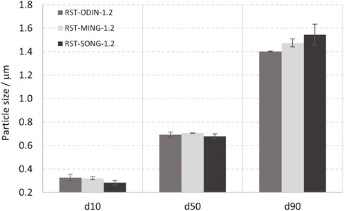
FIGURE 2. Particle size distribution D10, D50, and D90 corresponding to the percentages 10%, 50%, and 90% of particles under the reported particle size for the three different silicon kerf sources studied.
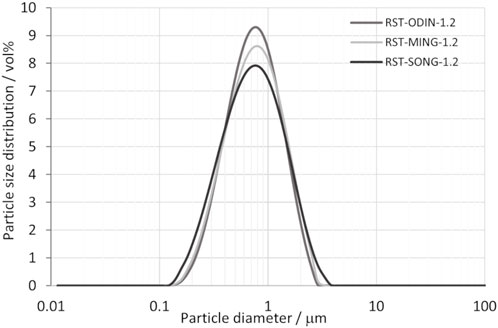
FIGURE 3. Particle size distribution as a function of particle diameter for the three different silicon kerf sources.
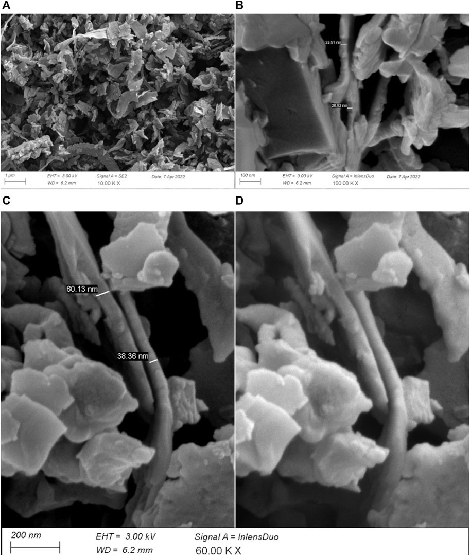
FIGURE 4. SEM images of RST-ODIN-1.3 showing the flake thickness of silicon kerf particles; (A) overview image with a secondary electron image at 10 K X; (B) detailing of silicon kerf flake thickness with an InLens Duo image at 100 K X; (C) detailing of silicon kerf thickness with a secondary electron image at 60 KX; and (D) same section as C with an InLens Duo image.
The analyses of dopants (Ga, B, and P) and light elements (C and O) are summarized in Table 2 for the three sources of silicon kerf, including the silicon kerf subjected to the pretreatment step prior to the drying step. Some variations are observed in the levels of boron and phosphorus, which can be related both to different resistivity targets of the suppliers and the type of silicon ingots produced (p- or n-type). The low values of gallium measured in the silicon kerf can be due to the low segregation coefficient for gallium (k0 = 0.008), which means that gallium is mostly incorporated toward the tail end of the crystals. For the metallic impurities, large variations exist, particularly for iron and aluminum, between the sources, as shown in Figure 5. Aluminum extends up to 0.7 wt% for one source, while for others, the values are as low as 8.5 ppmw. The main contributor to the aluminum content is the sacrificial beam material, where some producers use a beam material containing aluminum tri-hydroxide in a mix with polymethyl methacrylate (PMMA), while others use aluminum-free beam materials. Nickel contents are in the range 50–150 ppmw for the sources without the pretreatment step. The origin of nickel is the wire that is electroplated with nickel to attach the diamonds and is, therefore, difficult to avoid with the current technology. Titanium content is below 10 ppmw for all sources except the MING source, which has a level of 39 ppmw. This source also has a much higher level of iron than the other sources, which may be indicative of contamination from increased wire wear during wafering. The main metallic impurities measured in the silicon kerf powder samples (Al, Ni, and Fe) are all predominantly present as separate particles as they originate from the beam and wire materials. The contents of the metallic impurities in the silicon bulk are very low due to the strict requirements of the Cz-process for the silicon feedstock and the segregation toward the tail end of the crystal and the melt residue, which are not wafered and, thus, are not a part of the silicon kerf particles. In the study of Basnet et al. (2023), the levels of interstitial iron in industrially produced Cz-wafers with recharging (n-type) ranged from 3 × 10⁹ to 2 × 10¹⁰ at/cm3. The carbon contents for the silicon kerf samples varied from 1 to 4.4 wt%, while the oxygen content was more comparable between the sources that underwent step two (drying) and measured from 4 to 5 wt%. Comparing RST-ODIN-1.1 and RST-ODIN-1.2 showed that the pretreatment step (step one in Figure 1) is efficient in removing aluminum, nickel, and carbon from the silicon kerf.
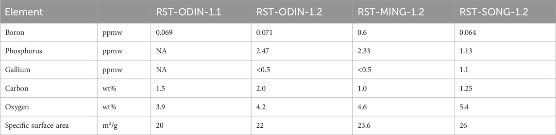
TABLE 2. ICP-MS (B), ICP-OES (Ga and P), and combustion analyses (C and O) for the different silicon kerf sources after process steps one and two and after process step two.
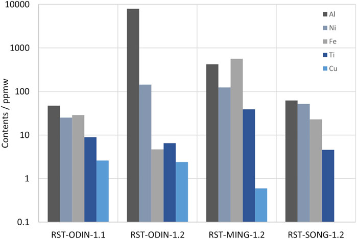
FIGURE 5. ICP-OES analyses of metallic impurities in different silicon kerf sources subjected to the processing detailed in Table 1.
The oxide layer thickness of the silicon kerf particles from step two of the process was determined by STEM-EELS. A thickness of 1–2 nm is measured on several silicon kerf particles after step two, as shown in Figure 6. The oxide layer covers the whole particle and has good uniformity, with a thickness variation estimated to be less than 0.5 nm from the STEM-EELS analysis. The thickness of 1–2 nm was also confirmed with XPS analyses on the same materials (Søiland et al., 2023).
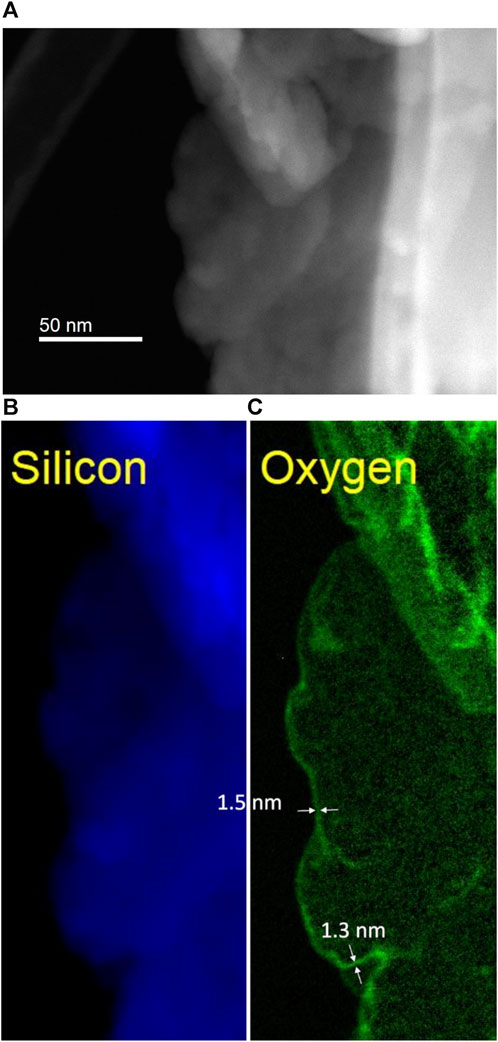
FIGURE 6. STEM-EELS imaging of the silicon kerf particle: (A); HAADF (High angle annular dark field) - STEM image (B) silicon signal; (C) oxygen signal and measured oxide layer thickness.
The initial capacities from the first discharge obtained for the different silicon materials range from 706 to 756 mAh/g, as shown in Figure 7. Both the highest and lowest values are obtained for the processed silicon kerf, where the RST-ODIN-1.3 shows the highest obtained capacity, while the RST-ODIN-1.4 shows the lowest initial capacity. The difference in the capacities between the two samples could be due to the additional surface treatment for RST-ODIN-1.4, which translates to lower silicon content by weight than that of the sample without the surface treatment. The capacities for the processed silicon kerf samples are on par with the reference samples, which range from 741 to 745 mAh/g. For the first cycle efficiencies, more variations exist between the different samples, which range from 86% to 93.2%, where the reference samples represent the extremes. The two processed silicon kerf samples lay at 89.5 and 90.7, where the sample RST-ODIN-1.4 has the highest value, which could be an effect of the surface treatment. All the cells were cycled at C/3 from 1.0 V to 50 mV vs. Li/Li+, and the specific capacities as a function of the cycle number are shown in Figure 8. The capacities for the cells are similar from cycle number 5 to approximately 75, except for reference 2, which exhibits higher capacities. Between cycle numbers 75 and 100, the reference cells and one of the silicon kerf cells show severe losses in capacities, which is not observed for the three other silicon kerf cells. This is clearer in the coulombic efficiency plots shown in Figure 9.
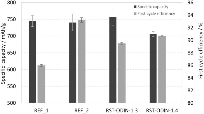
FIGURE 7. Average specific capacities after the first discharge and first cycle efficiencies for half-cells with the processed silicon kerf and reference silicon samples.
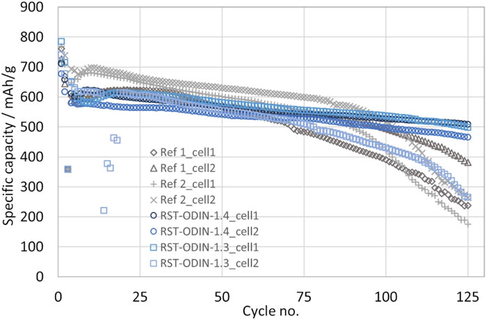
FIGURE 8. Specific capacity for half-cells with the processed silicon kerf and reference silicon samples as a function of cycle number; cycling rate after the formation cycles is C/3 and 1 V–50 mV vs. Li/Li+.
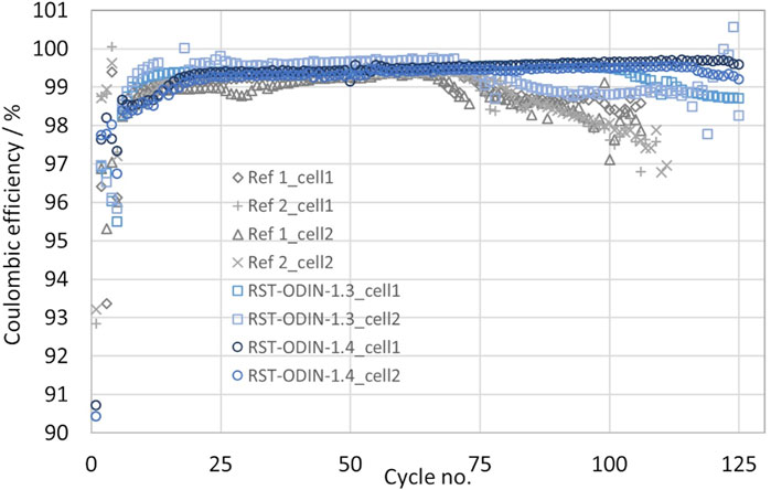
FIGURE 9. Coulombic efficiencies as a function of cycle number for the half-cells with the processed silicon kerf and reference silicon samples; cycling rate after formation cycles is C/3 and 1 V–50 mV vs. Li/Li+.
The silicon kerf has good homogeneity in terms of size and morphology between the sources studied. It can be considered both a micro- and nano-sized material due to its characteristic morphology, where one dimension is only a few tens of nanometers, while one other dimension can extend up to a few micrometers. Although there is less anisotropy in the silicon kerf and lower particle uniformity, it has similarities to one-D materials like silicon nanorods, nanotubes, and nanowires. These materials are specifically designed as anode materials for LIBs (Chan et al., 2008; Nguyen et al., 2011; Wu et al., 2012; Song et al., 2016; Tanaka et al., 2023), and the silicon kerf could, thus, be considered attractive based on the morphology/shape without necessarily further size reductions. Another distinctive factor of silicon kerf is the contents of the dopants dissolved within the silicon matrix. A phosphorus level of 3 ppmw will increase the electrical conductivity to ∼1.5 × 10³ S/m at RT compared to 1 × 10⁻² S/m for highly pure silicon (res ∼ 1 × 10⁴ Ω cm). A drawback of silicon as an anode material is the poor electrical conductivity; enhancing the transport of electrons for the silicon is, therefore, beneficial. The nickel impurities that are present in the silicon kerf powder as separate particles are also good electrical conductors (conductivity ∼1.4 × 10⁷ S/m at RT) and will be favorable for the transport of electrons in the anode. However, adverse effects related to electrolyte reactions of dissolved transition metals from cathodes in the anode solid electrolyte interphase (SEI) might be present (Blyr et al., 1998). Nevertheless, Ni is suggested to make a minimal contribution to anodic failure due to the hypothesis that reduced Ni on graphite surfaces does not decompose the electrolyte (Komaba et al., 2002). Depending on the temperature history of the silicon kerf, aluminum trihydroxide or alumina particles can also be present as separate particles in the silicon kerf. Since the atomic layer-deposited alumina has been used as a coating on silicon for enhancing the stability (Li et al., 2013; Li et al., 2023), it may be assumed that the alumina particles will have little lithium activity and form a stable layer with the electrolyte. However, the electrical conductivity is very low for the alumina particles and can impede the electron transport if present in larger amounts in the electrode. Both nickel and alumina can also be efficiently reduced by the developed pretreatment process. Concerning the crystallinity of silicon kerf, this has been thoroughly studied previously for similar silicon kerf sources, and it was shown that they are partly amorphous and partly crystalline, with up to 50% amorphous parts (Heintz et al., 2023).
The surface properties of the silicon kerf particles are crucial for the anode performance. Nano-sized spherical particles made by chemical vapor deposition of three different sizes of 50, 100, and 150 nm were studied by Zhu et al. (2019). They reported specific surface areas of 41.4, 36.11, and 7.33 m2/g, respectively. The second reference material in our study of size 80–100 nm has a specific surface area of 12–20 m2/g. In comparison, the silicon kerf particles have a specific surface area of 20–26 m2/g and, thus, seem comparable to a ∼100-nm-sized material in terms of surface area. This also seems valid when considering that a perfect sphere of the specific surface area 20 m2/g translates to a diameter of 130 nm. Therefore, the initial capacity losses for the silicon kerf samples due to SEI formation can be expected to be in a similar range as silicon materials of this size. Another aspect of the surface is the silicon oxide layer that spontaneously forms on bare silicon surfaces. The thickness of this silicon oxide layer is of importance for the transport of electrons and lithium ions. It is, thus, crucial that the processing conducted on the silicon kerf can control or limit the oxide layer thickness. For the silicon kerf subjected to process step two, the oxide layer thickness was measured between 1 and 2 nm with STEM-TEM, and it surrounded the entire particle. Xun et al. (2011) used XPS to measure an oxide layer thickness of 6.2 nm for chemical vapor-deposited nano-silicon and reported negative effects on the electrochemical performance, which were explained by the slowing down of the lithium-ion transport at the SiO2–Si interphase. Different SiO2 layer thicknesses on silicon and their impact on the electrochemical behavior were studied by Schnabel et al. (2020). They investigated thicknesses of 1–4 nm, where severe effects on the electrochemical behavior were observed for thicknesses above 3 nm. This led to the conclusion that a SiO2 layer of thickness below 3 nm is preferred to ensure high round-trip energy efficiency and high-rate capability. The silicon kerf after process step two with a measured oxide layer thickness of 1–2 nm is well within this critical thickness. It is not expected that process step three will influence the oxide layer thickness since this process is conducted at room temperature and under inert gas conditions.
The comparison study shows that the performance of the processed silicon kerf samples is comparable to that of the reference samples in terms of initial capacities, first cycle efficiencies, and cycling stability. The similarities in performance to the reference samples with a size of 40 and 100 nm further indicate that the size and morphology of the processed silicon kerf can be compared to a ∼100-nm-sized material without reducing the size of the silicon kerf particles. This is also highlighted by a similar specific surface area, as pointed out previously. Initial discharge capacities in the range 700–750 mAh/g are close to theoretical expectations for this slurry composition with 12 wt% Si (727 mAh/g-Si-Gr) and show that the initial silicon activity is high in all samples. Capacities that exceed the theoretically expected value can be due to SEI formation and side reactions known for silicon. For cycling stability, some differences are observed between the two references, where reference two is superior. From cycle number 80 to 100, both reference samples start to decay rapidly, while the majority of the processed silicon kerf samples still exhibit a slower decay, which is clearly observed in the coulombic efficiencies. The abrupt decay could be due to the complete depletion of the cyclable lithium in the cell, with the full consumption of the lithium metal counter electrode and the FEC in the electrolyte not being able to avoid the generation of mossy (dead) lithium.
Differential voltage analysis (DVA), also known as incremental capacity analysis (ICA), has been carried out at different cycling stages or state of health (SOH) in order to observe the evolution of the lithium-ion availability and silicon redox activity during the cycle life, as shown in Figure 10. The DVA consists of the analysis of dQ/dV as a function of voltage. It is a direct indicator of the state of health of the cell, as the experimental peaks are related to the active material chemical/structural evolution and redox reactions with Li+, such as phase transitions and recorded potential plateaus related to (de)intercalation reactions in graphite and (de)alloying with silicon during charging/discharging, deconvoluting their individual contributions, as identified by Heubner et al. (2022). The first formation cycle at a C/20 current rate (not shown here; see Supplementary Figure S1) differs from the rest in the peak positions of the electrode potential caused by the SEI formation and the irreversible structural changes of Si. On lithiation (negative axis), the first reduction peak at 200–300 mV corresponds to Li insertion into amorphous Si (a-Si), followed by two further Si reduction processes at 70 mV and 30 mV for the formation of a-LixSi and crystalline Li15Si4, respectively. Intercalation into graphite also occurs in this low range (67 mV and 27 mV), so the Li incorporation in Si and Gr is simultaneous in the 150–10-mV range. In contrast, distinct peaks are found below 150 mV for the oxidation reaction, which are exclusively attributed to the delithiation of Gr. Si starts to contribute above 250 mV and dominates above 300 mV. A compressed oxidation peak corresponds to the transition from amorphous Li3.16Si to Li2.33Si, and a more pronounced peak related to the dealloying of crystalline Li15Si4 is observed at ca. 450 mV. On cycling at C/3, the peaks are broader due to the higher current, but the resolution is good enough to follow the evolution of the silicon activity in the anodes from the first cycle (Figure 10A) through cycle 40 (Figure 10B), 80 (Figure 10C), and 120 (Figure 10D). The analysis indicates that Si activity is retained for all electrodes up to cycle 40, whereas beyond cycle 80, the first Si lithiation peak practically disappears in both the reference samples in agreement with the capacity decay observed for these cells. During oxidation, the final delithiation to the amorphous Si phase appears polarized at approximately 525 mV in the references vs. ∼475 mV in the ODIN samples, indicating a higher degree of pulverization of Si. By cycle 120, only the ODIN samples still retain slight Si activity, as observed in the flat oxidation peak at 500 mV, whereas the reference cells also lost graphite activity.
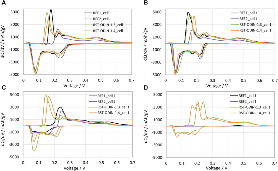
FIGURE 10. dQ/dV vs. voltage curves of the half-coin cells with different silicon samples at different C/3 cycles: (A) first cycle after the 2 formation cycles, (B) cycle number 40, (C) cycle 80, and (D) cycle 120.
The silicon kerf particles have a sub-micrometer size, with a measured d50 ∼700 nm, but are composed of flake-like particles of varying lengths, where one dimension is only a few tens of nanometers in thickness. In terms of specific surface area, the silicon kerf is more comparable to an ∼100-nm-sized silicon. The size distributions measured show little variation between the different sources of silicon kerf studied. The thickness of the silicon oxide layer surrounding the particles was measured to 1–2 nm.
The industrially processed silicon kerf was compared with nano-sized (40 nm and 100 nm) commercial silicon for LIBs in electrochemical testing in half-cell configuration. The initial specific capacities and first cycle efficiencies are comparable to the commercial silicon samples and close to the theoretical value, demonstrating a high silicon activity. The differential voltage analysis shows that the cycling stability is comparable between the two material types but reveals that only the silicon kerf cells maintain silicon activity beyond 120 cycles. These similarities in performance between the nano-sized commercial silicon and silicon kerf samples support the size considerations despite the differences that exist in morphology between the two silicon types. Since a negative impact on cell performance is expected with oxide layer thickness of above 3 nm, the obtained electrochemical data support the determined layer thickness from STEM-EELS.
This study shows that industrially processed silicon kerf can be a viable alternative to nano-sized silicon in the range of 100 nm as an anode material for LIBs, without any size reductions in the silicon kerf particles themselves. This can result in a silicon alternative with a low carbon footprint for the LIB industry. To further enhance the cycling stability, various concepts could be considered, such as silicon–carbon composite solutions, advanced electrode design for silicon materials with regard to binder systems/electrolyte additives, or coating the silicon kerf particles.
The original contributions presented in the study are included in the article/Supplementary Material; further inquiries can be directed to the corresponding author.
A-KS: conceptualization, formal analysis, investigation, methodology, project administration, visualization, writing–original draft, and writing–review and editing. IM: formal analysis, validation, writing–original draft, and writing–review and editing. AM: formal analysis, validation, investigation, and writing–review and editing. YX: investigation, visualization, and writing–review and editing. MB: investigation, validation, and writing–review and editing.
The author(s) declare that financial support was received for the research, authorship, and/or publication of this article. Part of this work received funding from the European Union’s Horizon 2020 research and innovation program under grant agreement 958365 (https://europa.eu/european-union/about-eu/symbols/flag_en).

The authors acknowledge the ICARUS project (HORIZON 2020; grant agreement ID: 958365) for the research funding.
Author A-KS was employed by ReSiTec AS.
The remaining authors declare that the research was conducted in the absence of any commercial or financial relationships that could be construed as a potential conflict of interest.
All claims expressed in this article are solely those of the authors and do not necessarily represent those of their affiliated organizations, or those of the publisher, the editors, and the reviewers. Any product that may be evaluated in this article, or claim that may be made by its manufacturer, is not guaranteed or endorsed by the publisher.
The Supplementary Material for this article can be found online at: https://www.frontiersin.org/articles/10.3389/fphot.2024.1332830/full#supplementary-material
An, W., Gao, B., Mei, S., Xiang, B., Fu, J., Wang, L., et al. (2019). Scalable synthesis of ant-nest-like bulk porous silicon for high-performance lithium-ion battery anodes. Nat. Commun. 10, 1447. doi:10.1038/s41467-019-09510-5
Basnet, R., Sun, C., Le, T., Yang, Z., Lui, A., Jin, Q., et al. (2023). Investigating wafer quality in industrial czochralski-grown gallium-doped p-type silicon ingots with melt recharging. Sol. RRL 7, 2023. doi:10.1002/solr.202300304
Blomeke, S., Arafat, R., Yang, J., Mai, J., Cerdas, F., and Herrmann, C. (2023). Environmental assessment of silicon kerf recycling and its benefits for applications in solar cells and Li-ion batteries, 30th CIRP Conference on Life Cycle Engineering. Procedia CIRP 116, 179–184. doi:10.1016/j.procir.2023.02.031
Blyr, A., Sigala, C., Amatucci, G., Guyomard, D., Chabre, Y., and Tarascon, J.-M. (1998). Self-discharge of LiMn2O4/C Li-ion cells in their discharged state. J. Electrochem. Soc. 145, 19. doi:10.1149/1.1838235
Chan, C., Peng, H., Liu, G., McIlwrath, K., Feng Zhang, X., and HugginsCui, R. A. Y. (2008). High-Performance lithium battery anodes using silicon nanowires. Nat. Nanotechnol. 3, 31–35. doi:10.1038/nnano.2007.411
Chen, C., Zhou, T., Danilov, D. L., Gao, L., Benning, S., Schön, N., et al. (2020). Impact of dual-layer solid-electrolyte interphase inhomogeneities on early-stage defect formation in Si electrodes. Nat. Commun. 11, 3283. doi:10.1038/s41467-020-17104-9
COM (2020). A new circular economy action plan for a cleaner and more competitive Europe, Brussels 11/3-2020. European Commission.
Drouiche, N., Cuellar, P., Kerkar, F., Medjahed, S., Boutouchent-Guerfi, N., and Hamou, M. O. (2014). Recovery of solar grade silicon from kerf loss slurry waste. Renew. Sustain. Energy Rev. 32, 936–943. doi:10.1016/j.rser.2014.01.059
Halvorsen, T., Moen, M., Mørk, K., Grosset-Bourbange, D., Rivat, P., Hajjaji, H., et al. (2017). “Cabriss recycling of Si-kerf from PV,” in 33rd European Photovoltaic Solar Energy Conference and Exhibition, Netherlands, 29 September 2017 (IEEE), 1524–1528.
He, Y., Jiang, L., Chen, T., Xu, Y., Jia, H., Yi, R., et al. (2021). Progressive growth of the solid-electrolyte interphase towards the Si anode interior causes capacity fading. Nat. Nanotechnol. 16, 1113–1120. doi:10.1038/s41565-021-00947-8
Heintz, M. C., Grins, J., Jaworski, A., Swensson, G., Thersleff, T., Brant, W., et al. (2023). Photovoltaic wafering silicon kerf loss as raw material: example of negative electrode for lithium-ion battery. ChemElectroChem 10 (Issue 19), 2023. doi:10.1002/celc.202300331
Hemetsberger, W., Schmela, M., and Cruz-Capellan, T. (2023). Global market outlook for solar power 2023-2027. Solar Power Europe.
Hengsong, J., Liu, Z., Li, X., Li, J., Jan, Z., and Tang, K. (2023). Recycling silicon waste from the photovoltaic industry to prepare yolk-shell Si@void@C anode materials for lithium-ion batteries. Processes 11 (6), 1764–1778. doi:10.3390/pr11061764
Heubner, C., Liebmann, T., Lohrberg, O., Cangaz, S., Maletti, S., and Michaelis, A. (2022). Understanding component-specific contributions and internal dynamics in silicon/graphite blended electrodes for high-energy lithium-ion batteries. Batter. Supercaps 5 (Issue 1), 2022. doi:10.1002/batt.202100182
Hu, Z., Zhao, R., Yang, J., Wu, C., and Bai, Y. (2023). Binders for Si based electrodes: current status, modification strategies and perspective. Energy Storage Mater. 59, 102776. doi:10.1016/j.ensm.2023.102776
Huang, J., Ye, L., Wu, M., Liu, H., Cui, Y., Lian, J., et al. (2023). Synthesis of Si/C composites by silicon waste recycling and carbon coating for high-capacity lithium-ion storage. Nanomaterials 13, 2142. doi:10.3390/nano13142142
IEA (2023). Global EV outlook 2023. Paris: IEA. Available at: https://www.iea.org/reports/global-ev-outlook-2023.
Jia, H., Li, X., Song, J., Zhang, X., He, Y., Li, B., et al. (2020). Hierarchical porous silicon structures with extraordinary mechanical strength as high-performance lithium-ion battery anodes. Nat. Commun. 11, 1474. doi:10.1038/s41467-020-15217-9
Jin, X., Kong, J., Zhou, X., Xing, P., and Zhuang, Y. (2020). Recycling of silicon kerf loss derived from diamond-wire saw cutting process to prepare silicon nitride. J. Clean. Prod. 247, 119163. doi:10.1016/j.jclepro.2019.119163
Kao, T.-L., Huang, W.-H., and Tuan, H.-Y. (2016). Kerf loss silicon as a cost-effective, high-efficiency, and convenient energy carrier: additive-mediated rapid hydrogen production and integrated systems for electricity generation and hydrogen storage. J. Mat. Chem. A 4, 12921–12928. doi:10.1039/c6ta03657k
Komaba, S., Kumagai, N., and Kataoka, Y. (2002). Influence of manganese(II), cobalt(II), and nickel(II) additives in electrolyte on performance of graphite anode for lithium-ion batteries. Electrochim. Acta 47, 1229–1239. doi:10.1016/S0013-4686(01)00847-7
Li, B., Yao, F., Bae, J. J., Chang, J., Zamfir, M. R., Le, D. T., et al. (2023). Hollow carbon nanospheres/silicon/alumina core-shell film as an anode for lithium-ion batteries. Sci. Rep. 5, 7659. doi:10.1038/srep07659
Li, J., Lin, Y., Wang, F., Shi, J., Sun, J., Ban, B., et al. (2021a). Progress in recovery and recycling of kerf loss silicon waste in the photovoltaic industry. Sp. Purif. Technol., 254. doi:10.1016/j.seppur.2020.117581
Li, J., Xiao, X., Cheng, Y.-T., and Verbrugge, M. W. (2013). Atomic layered coating enabling ultrafast surface kinetics at silicon electrodes in lithium-ion batteries. J. Phys. Chem. Lett. 4 (20), 3387–3391. doi:10.1021/jz4018255
Li, P., Kim, H., Myung, S.-T., and Sun, Y.-K. (2021b). Diverting exploration of silicon anode into practical way: a review focused on silicon-graphite composite for lithium ion batteries. Energy Storage Mater. 35 (2021), 550–576. doi:10.1016/j.ensm.2020.11.028
Liu, X. H., Zhong, L., Huang, S., Mao, S. X., Zhu, T., and Huang, J. Y. (2012). Size-dependent fracture of silicon nanoparticles during lithiation. ACS Nano 6 (2), 1522–1531. doi:10.1021/nn204476h
Ma, Q., Qu, J., Chen, X., Zhao, Z., Zhao, Y., Zhao, H., et al. (2020). Converting micro-sized kerf-loss silicon waste to high-performance hollow-structured silicon/carbon composite anodes for lithium-ion batteries. Sustain. energy fuels 9, 4780–4788. doi:10.1039/D0SE00831A
Muller, J., Michalowski, P., and Kwade, A. (2023). Impact of silicon content and particle size in lithium-ion battery anodes on particulate properties and electrochemical performance. Batteries 9 (7), 377. doi:10.3390/batteries9070377
Nguyen, H. T., Yao, F., Zamfir, M. R., Biswas, C., So, K. P., Hee Lee, Y., et al. (2011). Highly interconnected Si nanowires for improved stability Li-ion battery anodes. Adv. Energy Mat. 1, 1154–1161. doi:10.1002/aenm.201100259
Pastuszak, J., and Wegierek, P. (2022). Photovoltaic cell generations and current research directions for their development. Materials 15, 5542. doi:10.3390/ma15165542
Schnabel, M., Harvey, S. P., Arca, E., Stetson, C., Teeter, G., Ban, C., et al. (2020). Surface SiO2-thickness controls uniform-to-localized transition in silicon anodes for lithium-ion batteries. ACS Appl. Mat. Interfaces 12, 24. doi:10.1021/acsami.0c03158
Scott, D. M., and Matsuyama, T. (2014). Laser diffraction of acicular particles: practical applications. Int. Conf. Opt. Part. Charact. doi:10.1117/12.2067298
Søiland, A.-K., Mørk, K., and Heintz, M. C. (2023). Recycled silicon as potential anode material in Lithium-ion batteries, Poster at Advanced battery power conference in Aachen 27-28 April 2023.
Song, H., Wang, H. X., Lin, X., Jiang, X., Yu, L., Xu, J., et al. (2016). Highly connected silicon-copper alloy mixture nanotubes as high-rate and durable anode materials for lithium-ion batteries. Adv. Func. Mat. 26, 524–531. doi:10.1002/adfm.201504014
Tanaka, A., Otha, R., Dougakiushi, M., Tanaka, T., Takeushi, A., Fukuda, K., et al. (2023). Silicon nanorod formation from powder feedstock through co-condensation in plasma flash evaporation and its feasibility for lithium-ion batteries. Sci. Rep. 11, 22445. doi:10.1038/s41598-021-01984-y
Vorauer, T., Schöggl, J., Sanadhya, S. G., Poluektov, M., Widanage, W. D., Figiel, L., et al. (2023). Impact of solid-electrolyte interphase reformation on capacity loss in silicon-based lithium-ion batteries. Commun. Mater 4, 44. doi:10.1038/s43246-023-00368-1
Wagner, N. P., Tron, A., Tolchard, J. R., Noia, G., and Bellmann, M. P. (2019). Silicon anodes for lithium-ion batteries produced from recovered kerf powders. J. Power Sources 414, 486–494. doi:10.1016/j.jpowsour.2019.01.035
Wei, D., Gao, S., Kong, J., Jin, X., Jiang, S., Zhou, S., et al. (2020). Recycling silicon from silicon waste by Al-Si alloying. J. Clean. Prod. 251, 2020. doi:10.1016/j.jclepro.2019.119647
Wu, H., Chan, G., Choi, J. W., Ryu, I., Yao, Y., McDowell, M. T., et al. (2012). Stable cycling of double-walled silicon nanotube battery anodes through solid-electrolyte interphase control. Nat. Nanotechnol. 7 (5), 310–315. doi:10.1038/nnano.2012.35
Xu, Z., Yang, J., Li, H., Nuli, Y., and Wang, J. (2019). Electrolytes for advanced lithium-ion batteries using silicon-based anodes. J. Mater. Chem. A 16, 9432–9446. doi:10.1039/C9TA01876J
Xun, S., Song, X., Wang, L., Grass, M. E., Liu, Z., Battaglia, V. S., et al. (2011). The effects of native oxide surface layer on the electrochemical performance of Si nanoparticle-based electrodes. J. Electrochem. Soc. 158 (12), A1260–A1266. doi:10.1149/2.007112jes
Yang, Y., Wu, S., Zhang, Y., Liu, C., Wei, X., Luo, D., et al. (2021). Towards efficient binders for silicon based lithium-ion battery anodes. Chem. Eng. J. 406, 126807. doi:10.1016/j.cej.2020.126807
Zhao, X., and Lehto, V.-P. (2021). Challenges and prospects of nanosized silicon anodes in lithium-ion batteries. Nanotechnology 32, 042002. doi:10.1088/1361-6528/abb850
Zheng, S., Cheng, S., Fan, Z., and Wang, Z. (2022). Recycling of Si slurry as high performance anode materials for Lithium-ion batteries, Silicon for the chemical and solar industry XVI. doi:10.2139/ssrn.41177731
Keywords: silicon kerf loss, anode material, lithium-ion batteries, nano-sized silicon, recycled silicon, silicon oxide layer
Citation: Søiland A-K, de Meatza I, Muguruza A, Xu Y and Bellmann M (2024) Silicon kerf loss as a potential anode material for lithium-ion batteries. Front. Photonics 5:1332830. doi: 10.3389/fphot.2024.1332830
Received: 03 November 2023; Accepted: 29 January 2024;
Published: 22 February 2024.
Edited by:
Marisa Di Sabatino, Norwegian University of Science and Technology, NorwayReviewed by:
Sergio Pizzini, University of Milano-Bicocca, ItalyCopyright © 2024 Søiland, de Meatza, Muguruza, Xu and Bellmann. This is an open-access article distributed under the terms of the Creative Commons Attribution License (CC BY). The use, distribution or reproduction in other forums is permitted, provided the original author(s) and the copyright owner(s) are credited and that the original publication in this journal is cited, in accordance with accepted academic practice. No use, distribution or reproduction is permitted which does not comply with these terms.
*Correspondence: Anne-Karin Søiland, YWtzQHJlc2l0ZWMubm8=
Disclaimer: All claims expressed in this article are solely those of the authors and do not necessarily represent those of their affiliated organizations, or those of the publisher, the editors and the reviewers. Any product that may be evaluated in this article or claim that may be made by its manufacturer is not guaranteed or endorsed by the publisher.
Research integrity at Frontiers
Learn more about the work of our research integrity team to safeguard the quality of each article we publish.