
94% of researchers rate our articles as excellent or good
Learn more about the work of our research integrity team to safeguard the quality of each article we publish.
Find out more
REVIEW article
Front. Photonics, 10 January 2024
Sec. Photovoltaic Materials and Devices
Volume 4 - 2023 | https://doi.org/10.3389/fphot.2023.1331471
This article is part of the Research TopicUpgraded Metallurgical Grade (UMG) Silicon: Quality, Applications and Process EconomicsView all 5 articles
 Rabin Basnet*
 Daniel Macdonald
This review focuses on the challenges and potential pathways for utilizing upgraded metallurgical-grade silicon (UMG-Si) in the silicon photovoltaic industry. UMG-Si is an attractive low-cost alternative silicon feedstock, but its bulk quality is compromised due to the presence of defects and impurities. The review begins by identifying and discussing the various defects and impurities commonly found in UMG-Si wafers, drawing insights from a literature survey. The detrimental effects of these defects on solar cell performance are highlighted. Next, the review provides a summary of defect mitigation strategies that have been employed to improve the bulk quality of UMG-Si wafers. These strategies include tabula rasa, impurity gettering, and defect/impurity passivation through hydrogenation. The effectiveness of these strategies is evaluated by considering carrier lifetimes and comparing them with those of conventional silicon wafers. The review then examines the reported open-circuit voltages and efficiencies of solar cells based on UMG-Si wafers. A comparison is made between the performance of UMG-Si solar cells and those fabricated on conventional silicon. The impact of defect mitigation strategies on the performance of UMG-Si solar cells is discussed, emphasizing the improvements achieved through these strategies.
Upgraded metallurgical-grade silicon (UMG-Si) has long been considered as a viable alternative feedstock material for solar-grade silicon. The processing of UMG-Si involves several low-cost metallurgical techniques, in contrast to the energy-intensive Siemens process used in conventional polysilicon feedstock material. According to a recent estimate, UMG-Si boasts a 20% lower carbon footprint compared to chemically processed polysilicon (Méndez et al., 2021). Its low processing cost and capital expenditure (CAPEX) have positioned UMG-Si as a potential low-cost alternative to conventional polysilicon feedstock material. However, the dominance of Chinese polysilicon industries has resulted in a significant decrease in the spot price of standard polysilicon feedstock over the past decade, as shown in Figure 1. Recently, the spot price has experienced significant fluctuations due to an imbalance in supply and demand, reflecting the volatile nature of the market (Bernreuter, 2023), as shown in Figure 1. These current market conditions have posed a barrier to the adoption of alternative approaches, such as metallurgical purification, as feedstock materials for the Si-PV industry. Consequently, UMG-Si is facing challenges in establishing itself as a viable low-cost feedstock material.
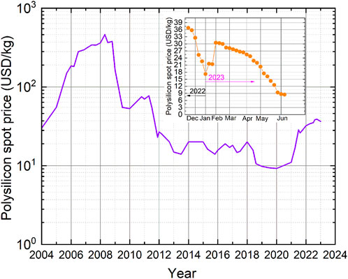
FIGURE 1. Monthly polysilicon spot price average from 2004 through 2023. The average monthly price of polysilicon in 2023 in shown in inset (Bernreuter, 2023).
Furthermore, it is widely known that UMG-Si contains significantly higher concentrations of metal impurities (iron, nickel, copper, etc.) and non-metal impurities (carbon and oxygen) compared to conventional electronic-grade silicon (EG-Si) (Bye and Ceccaroli, 2014). Consequently, the adoption of UMG-Si is further limited in the current Si-PV market, which demands high electronic quality of silicon wafers due to the emergence of several high-efficiency solar cell technologies. To remain relevant and competitive in the Si-PV market, it is crucial to enhance the electronic quality of UMG-Si wafers. One of the most common methods employed to achieve this is by implementing appropriate defect mitigation strategies. In recent years, significant progress has been made in developing a variety of defect mitigation strategies that target a wide range of defects and impurities. Detailed information on the progress of defect strategies can be found elsewhere (Wright et al., 2021; Liu et al., 2022; Song et al., 2022).
This review will first examine a brief history and purification processes of UMG-Si. It will then identify the relevant defects reported in UMG-Si wafers, followed by an examination of common mitigation strategies used to enhance their electronic quality (based on carrier lifetimes and open circuit voltage (Voc). Finally, the review will demonstrate the role of defect mitigation strategies in the evolution of solar cell performance based on UMG-Si wafers.
The detailed purification steps employed for producing polysilicon feedstock material is not the scope of this work, but can be found elsewhere (Delannoy, 2012; Li et al., 2017). Here we will only provide a brief overview of the process, as outlined in Figure 2. Metallurgical-grade silicon (MG-Si) are purified from silica ore by utilizing carbo-thermic reduction in submerged arc furnaces: SiO2

FIGURE 2. Schematic of process flows for the purification of polysilicon feedstock.
The conventional purification method employs a chemical routes as a modified Siemen’s process routes (Block and Wagner, 2000; Tilg and Mleczko, 2000; Corp, 2005; Dornberger, 2005; Corporation, 2006; Braga et al., 2008). The major modification is performed by increasing the production rate of the decomposition reactor. In addition, several production procedures and quality control are relaxed in comparison to the standard Siemens process. As a result, the cost of purification is lower for the SG polysilicon. However, relatively high concentrations of impurities are present in the SG purified polysilicon feedstock compared to, EG polysilicon, as shown in Table 1. Further, similar to the Siemens process, this route produces harmful chlorosilane compounds as by-products (Sørensen, 1998).
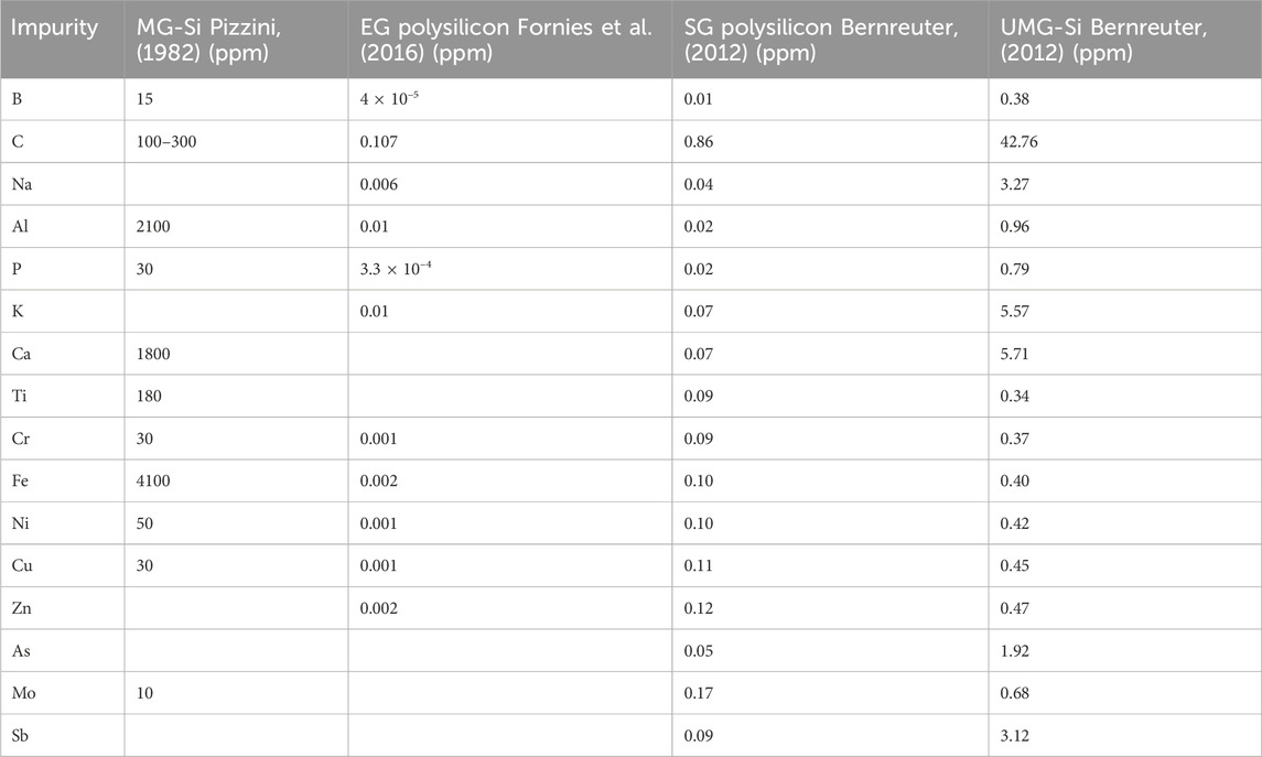
TABLE 1. Chemical characteristics of impurities in the different types of silicon feedstock material.
As an alternative to chemical refinement techniques, several metallurgical techniques are used to obtain SG-Si from MG-Si, as shown in Table 2. Unlike chemical route, in metallurgical route a specific metallurgical purification technique is not enough to reduce all impurity concentrations to an acceptable level. Therefore, metallurgical route contains multi-step purification process targeting different impurities based on different chemical and thermodynamic properties. SG-Si feedstock obtained via a metallurgical process is termed as upgraded metallurgical-grade silicon (UMG-Si). Several groups have employed different combinations of metallurgical refinement techniques to obtain UMG-Si feedstock, as shown in Table 2.
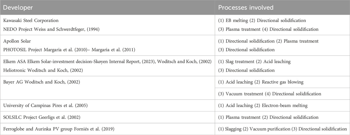
TABLE 2. Purification steps involved in the production of UMG-Si feedstock materials from different group.
Finally, silicon feedstock material is melted to crystalize silicon either to form multi-crystalline or mono-crystalline silicon ingots. Directional solidification or casting processes are used to grow multi-crystalline ingots. However, mono-crystalline silicon wafers are mostly grown using the Czochralski (Cz) method.
In the PHOTOSIL project (Einhaus et al., 2006; Margaria et al., 2010; Margaria et al., 2011), FerroPem, purified UMG-Si feedstock. This UMG-Si feedstock was then used to grow monocrystalline ingots through Czochralski silicon (Cz-Si) ingot growth as well as conventional multicrystalline silicon (mc-Si) by R&D companies like Apollon Solar and CEA-INES (France). Most of the reported works on UMG-Si wafers, such as from Apollon Solar, CEA-INES, The Australian National University (ANU), and University of New South Wales (UNSW), were based on PHOTOSIL project. Recently, the Aurinka PV group (Spain) has also reported some works on mc-Si based on 100% UMG-Si purified by FerroSolar group.
The incorporation of oxygen in Cz-Si is inevitable, and this leads to the formation of oxygen precipitate (OP) nuclei during the ingot cooling process. These OP nuclei act as recombination centers, compromising the bulk quality even in the as-grown state. The recombination activity of OP further increases during subsequent high-temperature processing, such as dopant diffusions and oxidations. Several studies have indicated that the recombination activity of OP originates either from dangling bonds (Lang et al., 2012; Koizuka and Yamada-Kaneta, 2000), impurities decorating OP, or OP-induced secondary defects (dislocations, stacking faults) (Seifert et al., 1995; Kirscht et al., 1996; Mchedlidze and Matsumoto, 1998; Murphy et al., 2013; Murphy et al., 2014). Extensive research by Murphy et al. (2014); Murphy et al. (2013); Murphy et al. (2011); Murphy et al. (2012); Murphy et al. (2015) has provided comprehensive insights into the recombination activity of OP in both n- and p-types of solar-grade Cz-Si wafers. These studies suggest that the recombination activity of OP enhances with increased surface area and becomes more pronounced when impurities decorate the OP.
The most common manifestation of OP-related defects is in the form of ring or disc-like defects, often observed after high-temperature processing of Cz-Si wafers. Ring defects, known for their high recombination activity, can cause a significant loss of efficiency of solar cells. UMG-Si, characterized by relatively high concentration of impurities like carbon (as shown in Table 1), is more susceptible to enhanced oxygen precipitation during high-temperature steps (Basnet et al., 2018; Basnet et al., 2020a; Basnet et al., 2021). Consequently, ring defects readily form in UMG-Cz-Si compared to electronic-grade (EG) Cz-Si wafers, given the same thermal budget. This significantly hampers the applicability of UMG-Cz-Si wafers in solar cells (homo-junction) fabrication unless appropriate defect mitigation strategies are incorporated. However, recent advancements have resulted in significant progress in achieving better control over oxygen incorporation during Cz-Si ingot growth. Cz-Si in mass production can now achieve interstitial oxygen concentration [Oi] as low as 12 ppm in n-type and 16 ppm in p-type ingots. UMG-Si grown using the current Cz-Si process is expected to exhibit lower [Oi] and potentially fewer OP-related defects compared to ingots grown few years ago.
Metal impurities significantly limit the efficiency of silicon solar cells. They act as recombination centers both in the form of point defects (as interstitial or substitutional atoms, or metal-acceptor pairs) and as precipitates. Generally, metallic impurities in silicon ingots can originate from feedstock materials, crucible, or puller parts and during device processing. As ingot growth conditions and polysilicon feedstock material have improved, conventional silicon wafers tend exhibit better control over impurity incorporation (Basnet et al., 2023). UMG-Si feedstock contains high levels of metallic impurities compared to silicon feedstock obtained by conventional Siemens process, as shown in Table 1. It is worth noting that the improvement in metallurgical purification and ingot pulling processes is expected to decrease the impurities concentrations in UMG-Si. However, it’s important to note that metallurgical purification involves multiple purification steps with different techniques, which may contribute to the variation in impurities concentrations. Nevertheless, the higher concentration of impurities in UMG-Si continues to reduce its electronic quality, making it unsuitable for current high-efficiency solar cells. This makes impurities-related defects are the most concerning for the adoption of UMG-Si in current the PV industry. Therefore, it is crucial to reduce impurity levels in UMG-Si by implementing appropriate gettering strategies.
LID caused by the presence of boron-oxygen (BO) pairs is known to decrease the long-term stability of solar cell performance, resulting in approximately 2% relative efficiency loss within the first year of module operation (Wolny et al., 2013; Hallam et al., 2017). However, the Si-PV industry has recently shifted from using boron (B) as the main dopant for p-type wafers to gallium (Ga) in order to avoid LID caused by BO pairs (VDMA, 2023). As a result, LID due to BO pairs is no longer a relevant defect in the current Si-PV industry.
However, the metallurgical purification processes have limitations when it comes to effectively eliminating doping elements such as boron and phosphorus compared to chemical distillation and condensation used in Siemens process, as shown in Table 1. Due to the high concentration of both donors and acceptors, UMG-Si is considered a “compensated” material and is susceptible to LID caused by BO pairs. Therefore, this review also briefly discusses defect mitigation strategies employed to address BO pairs.
Similarly, in the current Si-PV, there has been a shift away from cast-Si due to its inherent crystallographic defects, such as grain boundaries (VDMA, 2023). Therefore, any future developments related to UMG-Si should also focus on Cz-Si to remain relevant in the current market. However, some of the research, particularly from Spain-based Aurinka Solar are still primarily focused on UMG-mc-Si. The cost saving of over 40% per wafer offered by cast-Si compared to Cz-Si makes UMG-Si even more attractive material. Nevertheless, it is important to note that the perceived advantages of lower cost and environmental benefits will be negated if appropriate defect mitigation strategies are not applied to these wafers.
Tabula rasa (TR) is a high-temperature annealing process that has been used in the microelectronic industry to defect engineer OP-related defects by creating a “magic denuded zone” (Falster et al., 1997). However, this step has also been slowly used in solar cells research to mitigate bulk degradation (Basnet et al., 2018; Ochoa et al., 2020; LaSalvia et al., 2019). It is commonly used as a pre-fabrication process to improve bulk quality by minimizing thermal history (dissolving grown-in OP nuclei or metal precipitates) in Cz-Si wafers (Basnet et al., 2018; Basnet et al., 2019; LaSalvia et al., 2019; Basnet et al., 2020b), as shown in Figure 3. The schematic illustrates that the TR step dissolves grown-in OP nuclei, making the samples free of OP nuclei, as represented by the middle block. Following subsequent high-temperature processing, the sample subjected to Tabula Rasa shows reduced growth of OPs compared to the one without the TR treatment.
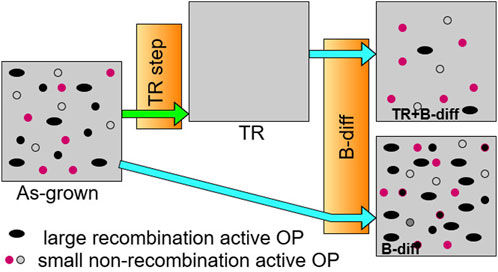
FIGURE 3. Schematic of tabula rasa process, which dissolves grown-in OP nuclei (as represented by middle block). Then, after subsequent high-temperature processing, OPs will grow lesser than in the sister sample without TR.
The application of the TR step had a significant impact on the carrier lifetime of the n–type UMG-Cz-Si wafers from the PHOTOSIL project, as shown in Figure 4. The as-grown samples, which did not undergo any TR step (t = 0 min), exhibited much lower carrier lifetimes
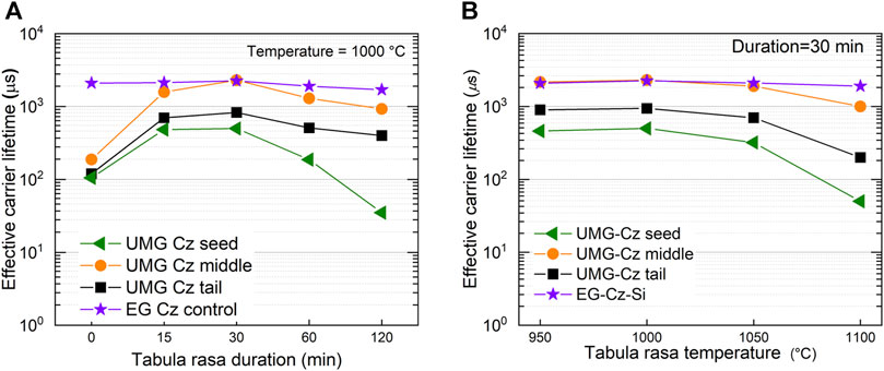
FIGURE 4. Effective carrier lifetimes at an injection
Figure 5A demonstrates the benefits of a TR step when samples underwent boron diffusion, which is necessary for junction formation in n-type UMG-Si wafers. Two sets of the UMG-Cz-Si and EG-Cz-Si samples, consisting of as-grown (no TR) and TR-treated, were subjected to boron diffusion. After boron diffusion process, the effective carrier lifetimes of both the as-grown samples reduced (τas-grown > τB-diff). However, a reduction in lifetime was significantly higher in UMG-Cz-Si compared to EG-Cz-Si samples, indicating that UMG-Cz-Si wafers were more prone to degradation than EG-Cz-Si under the same high-temperature processes. Nonetheless, when the samples were treated with TR prior to boron diffusion, the degradation was significantly reduced (τas-grown < τTR+B-diff), particularly in UMG-Cz-Si samples.
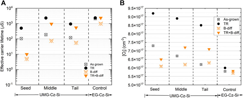
FIGURE 5. Evolution of the effective lifetimes (at an injection level of
Additionally, interstitial oxygen concentration [Oi], measured by Fourier-transform infrared spectroscopy (FTIR) showed a significant increase after TR step in UMG-Cz-Si compared to EG-Cz-Si, as shown in Figure 5B. This suggests that UMG-Cz-Si initially had high concentrations of grown-in OP nuclei, which further grew and became more recombination active during boron diffusion, resulting in reduced effective lifetimes. The dissolution of grown-in OP nuclei through TR helped to improve bulk quality of UMG-Cz-Si, making it more resilient to degradation during subsequent boron diffusion. This concept of employing TR as a pre-fabrication treatment was utilized to fabricate tunnelling oxide passivated contact (TOPCon) solar cells based on n-type UMG-Cz-Si wafers, achieving a record solar cell efficiency of 22.6% (Basnet et al., 2019), also refer Table 4. In the same batch, cells without the TR step, highly recombination active ring defects appeared and experienced a loss of over 50 mV of implied open-circuit voltage (iVoc).
It has been observed that the benefit of the TR step is not permanent but only delays the onset of ring defects during subsequent high-temperature processes (Basnet et al., 2020a). The incubation duration for ring defects formation depends on the bulk quality of samples and the thermal conditions. Generally, the onset of ring defects occurs faster in UMG-Cz-Si samples than in EG-Cz-Si samples with the same thermal budget. The presence of high concentrations of impurities, such as carbon and metal impurities enhances the growth of OP (Zhang et al., 2015; Shimura, 1986) and accelerates the formation of ring defects in the UMG-Cz-Si. TR poses challenges due to requirement of high temperature (>1,000°C), leading to increased processing costs and introducing a notable risk of contamination for industry. Therefore, optimization of the thermal budget during the fabrication process is crucial for maintaining the bulk quality of any UMG-Cz-Si wafers than adapting a TR step in industrial application.
Gettering is the one of most common form of defect mitigation method which helps to relocate mobile metal impurities, such as interstitial iron from the bulk of silicon to a region in the device where they have a less harmful impact on the device performance. Typically, phosphorus diffusion performed to form an n+ region in traditional p-type passivated emitter and rear cells (PERC) or aluminium back surface field (Al-BSF) solar cells, provides gettering effect that can reduce interstitial iron concentration by more than two orders of magnitude. Additionally, recent works have demonstrated that passivating contacts based on doped polysilicon layers (both polarities) are known to provide strong gettering effects (Yang et al., 2023; Hayes et al., 2019).
The effectiveness of gettering depends on finding a balance between impurity diffusion and their segregation to the sink layer (diffused layers). Higher temperatures promote impurity diffusion towards the sink layer but reduce segregation, while lower temperatures enhance segregation to the sink. It is important to optimize the gettering thermal budget not only for impurity removal but also to mitigate other forms of bulk degradation. In some cases, high-temperature gettering processes can activate grown-in defects such as OP, leading to a severe reduction in carrier lifetime. As result, most works on UMG-Si wafers have used a lower temperature range (around 780°C) compared to conventional phosphorus diffusion (≥800°C) (Basnet et al., 2018; Catalán-Gómez et al., 2022). Additionally, the gettering effectiveness in UMG-Si wafers have been found to be enhanced by extending the duration or employing a two-step PDG process (Dasilva-Villanueva et al., 2023), as shown in Figure 6. Dasilva-Villanueva et al. (2023) reported an effective carrier lifetime values up to 645 µs ( at an injection level of 1
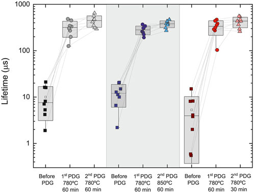
FIGURE 6. Effective lifetime variation of the samples [at an injection level of 1
Therefore, optimization of the gettering process for UMG-Si wafers should consider a trade-off between the process parameters and impurity behaviour. Furthermore, the bulk degradation during phosphorus diffusion getterting can be mitigated by combining with it with either a TR or H to achieve the most effective improvement in bulk quality, known as a TR+PDG or PDG+H steps, respectively, as shown in Table 3.
TABLE 3. Elucidation of impact of the defect mitigation strategies on carrier lifetimes of UMG-Si wafers used in different works with corresponding EG-Si used as a control.
Hydrogen passivation, also known as hydrogenation, is widely used defect engineering process in silicon solar cell fabrication. It involves annealing hydrogen-rich dielectric films, such as SiNx:H, AlOx:H, and a-Si:H, at a moderate temperature range (typically
Hydrogenation is typically performed by annealing the samples in a tube furnace, hotplate, or rapid thermal annealing, with or without illumination. Its passivation effectiveness is highly dependent on whether it is used in isolation or in combination with other methods such as TR and PDG.
In the case of UMG-Cz-Si wafers, hydrogenation is commonly used for passivating OP-related defects. It can effectively passivate ring defects that are formed during high-temperature processing, as shown in Figure 7. Generally, hydrogenation is most effective when combined with TR and PDG for the passivation of ring defects and grown-in OP nuclei in UMG-Si wafers (Basnet et al., 2018). It is important to note that the impact of hydrogenation also depends on the ingot position. Additional optimization of hydrogenation conditions may be required when dealing with higher defect densities of different types of defects. It is believed that in the seed-end of Cz ingot, vacancy-related defects are also present along with OP-related.
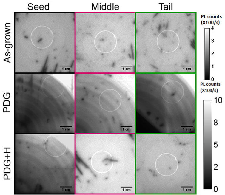
FIGURE 7. PL images of the UMG-Cz-Si wafers from three different positions of the ingot which show the effect of PDG and PDG+H compared to the as-grown state. A scale bar shown in the first row is for the as-grown samples and in the second row is for all other samples. All of the images were captured at constant illumination intensity of 0.5 suns and normalized to PL counts/second. The bright circle in the images is an artefact due to the conductance coil in the PL imaging tool (Basnet et al., 2018).
Hallam et al. (2015) proposed an advanced hydrogenation process that involves laser illumination. This process can manipulate hydrogen charge states, enhancing the passivation effectiveness of defects such as BO pairs, oxygen precipitates and grain boundaries. This advanced hydrogenation process offers improved passivation capabilities compared to traditional hydrogenation methods.
Vicari Stefani et al. (2019) conducted a study on the utilization of advanced hydrogenation combined with a PDG step (PDG+H) to improve the bulk quality of p-type UMG-mc-Si wafers. They found that hydrogenation alone did not significantly improve the bulk quality. However, when combined with a PDG step (PDG+H), a remarkable improvement in carrier lifetime was achieved, as illustrated in Figure 8A. When the hydrogenation process was applied to a previously gettered sample, the recombination activity of most grain boundaries decreased significantly. Additionally, an improvement in the intra-grain regions was observed, as well as the passivation of a fraction of defects gettered to the dislocation clusters during gettering. The increased effectiveness of hydrogenation after the gettering treatment can be attributed to the removal of metallic impurities, including interstitial iron (Fei), and complexes such as iron-oxygen (Fe–O) and iron-boron (Fe–B) during the gettering step. By eliminating these impurities, more hydrogen became available for passivating the grain boundaries during the subsequent hydrogenation process. Further, the carrier lifetimes of UMG-mc-Si samples were compared after normalizing to their resistivity. After normalization, UMG-mc-Si samples exhibited similar carrier lifetimes to conventional mc-Si samples, as shown in Figure 8B. Furthermore, in the same study, the PDG+H process was employed as a pre-fabrication step to fabricate a silicon heterojunction (SHJ) solar cell based on p-type UMG-mc-Si wafers. This approach resulted in a record Voc of 690 mV, demonstrating the effectiveness of the combined PDG+H process in enhancing the performance of solar cells fabricated from UMG-mc-Si wafers. This achievement is also presented in Table 4, which summarized the Voc and efficiencies of solar cells based on UMG-Si wafers from various studies. Consequently, gettering and hydrogenation emerge as the two most promising strategies for enabling high-efficiency UMG-Si solar cells. Although these strategies are standard processes in current industrial cells, the need for extended gettering steps (such as 2-step or slow ramp-down) may be constrained by the current throughput rate of the industry.
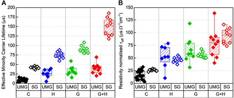
FIGURE 8. Impact of the defect mitigation strategies in (A) the effective minority carrier lifetime and (B) resistivity normalized effective minority carrier lifetime on both p-type UMG-mc-Si and solar-grade multi-crystalline silicon (SG-mc-Si) wafers. The wafers are divided in four groups, according to the defect mitigation strategies processes applied: non-gettered and non-hydrogenated control wafers (C), gettered (G) wafers, hydrogenated wafers (H), and gettered + hydrogenated wafers (G + H) (Vicari Stefani et al., 2019).
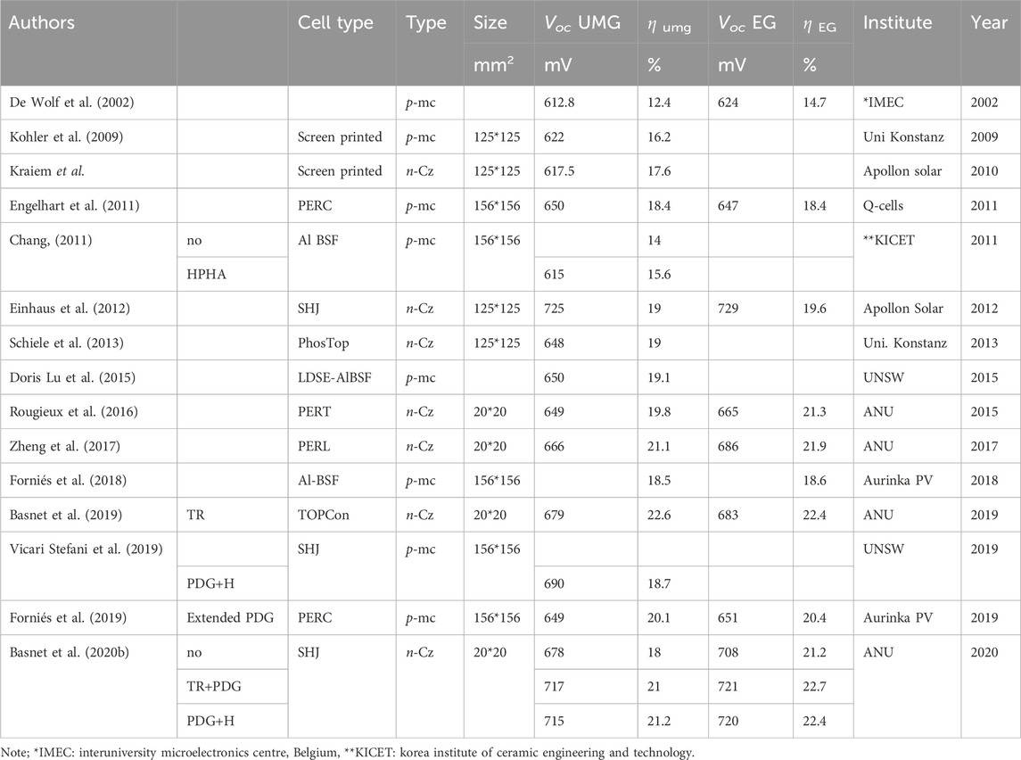
TABLE 4. A comparison of reported performance of solar cells based on UMG-Si (Cz and mc) wafers and corresponding conventional silicon wafers used as a control. It also includes Voc, resistivities of wafers, cell structure, and any defect mitigation strategies employed.
Hydrogenation has been also employed to permanently deactivate BO pairs in compensated UMG-Cz-Si solar cells. Previous works on the deactivation of BO pairs in compensated silicon had shown inconsistent until Sun et al. (2018) demonstrated the complete regeneration of BO defects in n-type UMG-Cz-Si based SHJ solar cells. In their study, hydrogen from a-Si:H layers was utilized to deactivate BO pairs in compensated UMG-Cz-Si cells, resulting in a fast and complete regeneration of BO pairs under 93 suns at 220°C.
Table 3 provides a summary of various defect mitigation strategies used either in isolation or in combination to improve the material quality of UMG-Si (Cz and mc) wafers. The improvement in bulk quality is quantified by effective lifetimes measured at an injection level of
Hydrogenation passivation can be sensitive to subsequent high temperature (>650°C) processes, as the elevated temperatures can cause hydrogen effusion from the bulk of the material (Sopori et al., 2002), leading to a loss of passivation efficacy. Therefore, it is important to perform hydrogenation after all the high-temperature processes to ensure its stability.
To address the issue of hydrogenation stability at higher temperatures, some recent works have proposed fluorination as an alternative passivation method. Fluorine-containing films, such as magnesium fluoride (MgFx) have been used for fluorination (Sio et al., 2023; Basnet et al., 2022). Fluorination has shown promise in passivating ring defects in n-type UMG-Cz-Si, and it has been observed that fluorine passivated ring defects exhibit slower de-passivation kinetics compared to hydrogen-passivated ring defects. This suggests that fluorine passivation can offer greater stability than hydrogen passivation of ring defects during subsequent heat treatments.
Table 4 summarizes the Voc and efficiency (η) of UMG-Si solar cells obtained from various studies, including comparisons with EG-Si solar cells used as controls in the corresponding batches. In earlier works, solar cells based on UMG-Si wafers were primarily aluminum back surface field (Al-BSF) structure, which has inherent limitations in efficiency. As a result, the cell efficiencies were low, and the Voc for both control and UMG-Si cells were similar.
However, when a high efficiency solar cell structures such as passivated emitter and rear totally diffused (PERT) and passivated emitter with rear locally diffused (PERL) were employed, the efficiency of UMG-Si solar cells also increased (Zheng et al., 2017), Rougieux et al. (2016). Zheng et al. (2017) achieved a record UMG-Si solar cell efficiency of 21.1% in 2017. In these works, the Voc of the UMG-Cz-Si cells were nearly 20 mV lower than the control solar cells, resulting in >0.8% (abs) loss in efficiencies. This indicates that the bulk quality of UMG-Cz-Si wafers is a significant limiting factor for achieving higher efficiencies when used in the high-efficiency solar cell structures.
To address the low bulk lifetime and mitigate bulk degradation of UMG-Cz-Si wafers, appropriate defect mitigation strategies such as TR, PDG and hydrogenation have been employed. These strategies have been instrumental in achieving a current record efficiency for UMG-Cz-Si solar cells based on TOPCon and SHJ structures (Basnet et al., 2019), Basnet et al. (2020b). In the case of TOPCon structure, TR was incorporated as a pre-treatment step to mitigate the bulk degradation during subsequent high temperature processes, such as boron diffusion and TOPCon layers formation. Further, gettering effect provided by phosphorus doped polysilicon layers helped to mitigate the impact of metal impurities (Yang et al., 2023), Hayes et al. (2019). The combined effect of TR and gettering effects and better passivation by TOPCon layers helped to achieve a similar Voc of 679 mV and 683 mV for solar cells based on UMG-Cz-Si and EG-Cz-Si, respectively.
For the SHJ structure, pre-fabrication treatments such as such as TR+PDG and PDG+H were utilized to enhance the bulk quality of UMG-Cz-Si, resulting in significant improvements in Voc (>30 mV) and efficiency (>3% absolute) compared to the as-grown cells. Interestingly, EG-Cz-Si also exhibited improvements with pre-fabrication treatments. Nevertheless, the Voc of UMG-Cz-Si solar cells were comparable to those of the EG-Cz-Si solar cells. This indicates that UMG-Cz-Si can be a competitive alternative to EG-Cz-Si, if appropriate defect engineering steps are implemented during solar cell fabrication.
Furthermore, Forniés et al. (2019) demonstrated a record efficiency of p-type UMG-mc-Si utilizing PERC technology. The work had employed an extended PDG step to improve the gettering effectiveness. UMG-mc-Si solar cells achieved 20.1% efficiency and the control cells based on conventional mc-Si achieved 20.4%. However, the study did not mention the gain in efficiency achieved by using extended PDG step.
In summary, the development and implementation of defect mitigation strategies has shown promising results in improving the bulk quality of current UMG-Si wafers. Several methods such as tabula rasa, gettering and hydrogenation have been utilized and optimized to mitigate various defects and impurities present in UMG-Si. These strategies have led to improvements in carrier lifetime, Voc and efficiency of solar cells based on UMG-Si wafers. While UMG-Si wafers are low quality compared to conventional silicon wafers, advancements in UMG-Si purifications and ingot growth processes are expected to further enhance the quality of UMG-Si in the future. By optimizing defect mitigation strategies, the performance of UMG-Si based solar cells are expected to further improve to be competitive with conventional silicon solar cells, indicating the potential of UMG-Si as a viable alternative. However, it is important to conduct detailed techno-economic studies to evaluate true advantages of defect mitigation strategies and fully exploit the cost and environmental benefits of UMG-Si. Continued research and development efforts in purification steps and defect mitigation strategies will contribute to the advancement and wider adoption of UMG-Si in the Si-PV industry.
RB: Conceptualization, Data curation, Investigation, Methodology, Resources, Visualization, Writing–original draft, Writing–review and editing. DM: Funding acquisition, Supervision, Writing–review and editing.
The author(s) declare financial support was received for the research, authorship, and/or publication of this article. This work has been supported by the Australian Renewable Energy Agency (ARENA) through the Australian Centre for Advanced Photovoltaics (ACAP), and project 2022/TRAC004 and 2022/TRAC005.
The authors declare that the research was conducted in the absence of any commercial or financial relationships that could be construed as a potential conflict of interest.
All claims expressed in this article are solely those of the authors and do not necessarily represent those of their affiliated organizations, or those of the publisher, the editors and the reviewers. Any product that may be evaluated in this article, or claim that may be made by its manufacturer, is not guaranteed or endorsed by the publisher.
Basnet, R., Phang, S. P., Samundsett, C., Yan, D., Liang, W., Sun, C., et al. (2019). 22.6% efficient solar cells with polysilicon passivating contacts on n-type solar-grade wafers. Sol. RRL 3 (11), 1900297. 22. doi:10.1002/solr.201900297
Basnet, R., Phang, S. P., Sun, C., Rougieux, F. E., and Macdonald, D. (2020a). Onset of ring defects in n-type Czochralski-grown silicon wafers. J. Appl. Phys. 127 (15), 153101. doi:10.1063/5.0005899
Basnet, R., Rougieux, F. E., Sun, C., Phang, S. P., Samundsett, C., Einhaus, R., et al. (2018). Methods to improve bulk lifetime in n-type czochralski-grown upgraded metallurgical-grade silicon wafers. IEEE J. Photovoltaics 8 (4), 990–996. doi:10.1109/JPHOTOV.2018.2834944
Basnet, R., Sio, H., Siriwardhana, M., Rougieux, F. E., and Macdonald, D. (2021). Ring-like defect formation in N-type czochralski-grown silicon wafers during thermal donor formation. Phys. status solidi 218 (4), 2000587. doi:10.1002/pssa.202000587
Basnet, R., Sio, H. C., Sun, C., Nguyen, H. T., and Macdonald, D. (2022). Passivation of ring defects in czochralski-grown silicon using magnesium fluoride films. ACS Appl. Energy Mater. 5 (8), 9877–9884. –9884. doi:10.1021/acsaem.2c01550
Basnet, R., Sun, C., Le, T., Yang, Z., Jin, Q., et al. (2023). Investigating wafer quality in industrial czochralski-grown gallium-doped p-type silicon ingots with melt recharging. Sol. RRL 7. doi:10.1002/solr.202300304
Basnet, R., Weigand, W., Yu, Z. J., Sun, C., Phang, S. P., Sio, H. C., et al. (2020b). Impact of pre-fabrication treatments on n-type UMG wafers for 21% efficient silicon heterojunction solar cells. Sol. Energy Mater. Sol. Cells 205, 110287. doi:10.1016/j.solmat.2019.110287
Bernreuter, J. (2012). “Polysilicon production technologies in a volatile market,” in Photovoltaics international. 18th edn, 29–32.
Bernreuter, J. (2023). Polysilicon price trend. [Online]. Available at: https://www.bernreuter.com/polysilicon/price-trend/.
Block, H., and Wagner, G., “The bayer route to low cost solar grade silicon,” in 16th Eur. Photovoltaic Solar Energy Conf, 2000, pp. 1–6.
Braga, A. F. B., Moreira, S. P., Zampieri, P. R., Bacchin, J. M. G., and Mei, P. R. (2008). New processes for the production of solar-grade polycrystalline silicon: a review. Sol. Energy Mater. Sol. Cells 92, 418–424. doi:10.1016/j.solmat.2007.10.003
Bye, G., and Ceccaroli, B. (2014). Solar grade silicon: technology status and industrial trends. Sol. Energy Mater. Sol. Cells 130, 634–646. doi:10.1016/j.solmat.2014.06.019
Catalán-Gómez, S., Dasilva-Villanueva, N., Marrón, D. F., and del Cañizo, C., “New insights into upgraded metallurgical grade silicon wafers through lifetime spectroscopy,” 2022, p. 130002. doi:10.1063/5.0089685
Chang, H. S. (2011). Effect of passivation process in upgraded metallurgical grade (UMG)-silicon solar cells. Sol. Energy Mater. Sol. Cells 95 (1), 63–65. doi:10.1016/j.solmat.2010.05.018
Corp, T. (2005). Responsible care & eco management department tokuyama corporation-responsible care report.
Dasilva-Villanueva, N., Arıkan, B., Canar, H., Fuertes Marrón, D., Hong, B., Keçeci, A., et al. (2023). High carrier lifetimes in UMG multicrystalline wafers after P- diffusion compatible with high-efficiency cell structures. Sol. Energy Mater. Sol. Cells 250, 112080. doi:10.1016/j.solmat.2022.112080
Delannoy, Y. (2012). Purification of silicon for photovoltaic applications. J. Cryst. Growth 360, 61–67. doi:10.1016/j.jcrysgro.2011.12.006
De Wolf, S., Szlufcik, J., Delannoy, Y., Périchaud, I., Häßler, C., and Einhaus, R. (2002). Solar cells from upgraded metallurgical grade (UMG) and plasma-purified UMG multi-crystalline silicon substrates. Sol. Energy Mater. Sol. Cells 72 (1–4), 49–58. doi:10.1016/S0927-0248(01)00149-0
Doris Lu, P. H., Hallam, B., Chan, C., Wenham, A., Abbott, M., Chen, D., et al. (2015). “19.1 % laser-doped selective emitter P-type multi-crystalline UMG silicon solar cell,” in 2015 IEEE 42nd Photovoltaic Specialist Conference (PVSC) (IEEE), 1–5. doi:10.1109/PVSC.2015.7355746
Einhaus, R., Kraiem, J., Cocco, F., Caratini, Y., Bernou, D., Sarti, D., et al. (2006). “PHOTOSIL – simplified production of solar silicon from metallurgical silicon,” in 23th European Photovoltaic Solar Energy Conference (Dresden, Germany: Dresden), 580–583.
Einhaus, R., Kraiem, J., Degoulange, J., Nichiporuk, O., Forster, M., Papet, P., et al. (2012). “19% efficiency heterojunction solar cells on Cz wafers from non-blended Upgraded Metallurgical Silicon,” in 2012 38th IEEE Photovoltaic Specialists Conference (IEEE), 003234–003237. doi:10.1109/PVSC.2012.6318266
Elkem Solar-investment decision-Skøyen Internal Report (2023)“Elkem solar-investment decision-skøyen internal report.”
Engelhart, P., Wendt, J., Schulze, A., Klenke, C., Mohr, A., Petter, K., et al. (2011). R&D pilot line production of multi-crystalline Si solar cells exceeding cell efficiencies of 18%. Energy Procedia 8, 313–317. doi:10.1016/j.egypro.2011.06.142
Falster, R. J., Cornara, M., Gambaro, D., Olmo, M., and Pagani, M. (1997). Effect of high temperature pre-anneal on oxygen precipitates nucleation kinetics in Si. Solid State Phenom. 57 (58), 123–128. doi:10.4028/www.scientific.net/SSP.57-58.123
Forniés, E., del Cañizo, C., Méndez, L., Souto, A., Pérez Vázquez, A., and Garrain, D. (2021). UMG silicon for solar PV: from defects detection to PV module degradation. Sol. Energy 220, 354–362. doi:10.1016/j.solener.2021.03.076
Forniés, E., Ceccaroli, B., Méndez, L., Souto, A., Pérez Vázquez, A., Vlasenko, T., et al. (2018). “Performance of modules and solar cells made of 100% solar silicon purified by direct route,” in 35th European Photovoltaic Solar Energy Conference and Exhibition (Brussels, Belgium: EU PVSEC), 473–475.
Fornies, E., Mendez, L., and Tojeiro, M. (2016). Polysilicon vs. upgraded metallurgical-grade silicon (UMG-Si): technology, quality and costs. Photovolt. Int. Brussels, Belgium.
Forniés, E., Ceccaroli, B., Méndez, L., Souto, A., Pérez Vázquez, A., Vlasenko, T., et al. (2019). Mass production test of solar cells and modules made of 100% UMG silicon. 20.76% record efficiency. Energies 12 (8), 1495. doi:10.3390/en12081495
Geerligs, L., Wyers, G., Jensen, R., Raaness, O., Waernes, A. N., Santén, S., et al. (2002). “Solar-grade silicon by a direct route based on carbothermic reduction of silica: requirements and production technology,” .
Hallam, B., Chan, C., Abbott, M., and Wenham, S. (2015). Hydrogen passivation of defect-rich n-type Czochralski silicon and oxygen precipitates. Sol. Energy Mater. Sol. Cells 141, 125–131. doi:10.1016/j.solmat.2015.05.009
Hallam, B., Eadie, M., Sugianto, A., Wenham, S. R., Casalenuovo, K., Kraiem, J., et al. (2012). “High quality passivation for p-type CZ UMG silicon wafers,” in 27th European Photovoltaic Solar Energy Conference and Exhibition, Frankfurt, 1942–1945. doi:10.4229/27thEUPVSEC2012-2CV.6.53
Hallam, B., Kim, M., Abbott, M., Nampalli, N., Nærland, T., Stefani, B., et al. (2017). Recent insights into boron-oxygen related degradation: evidence of a single defect. Sol. Energy Mater. Sol. Cells 173, 25–32. doi:10.1016/j.solmat.2017.06.038
Hayes, M., Martel, B., Alam, G. W., Lignier, H., Dubois, S., Pihan, E., et al. (2019). Impurity gettering by boron- and phosphorus-doped polysilicon passivating contacts for high-efficiency multicrystalline silicon solar cells. Phys. status solidi 216 (17), 1900321. doi:10.1002/pssa.201900321
Kirscht, F. G., Furukawa, Y., Seifert, W., Schmalz, K., Buczkowski, A., Kim, S., et al. (1996). Electrical characteristics of oxygen precipitation related defects in Czochralski silicon wafers. Mater. Sci. Eng. B 36 (1–3), 230–236. doi:10.1016/0921-5107(95)01289-3
Kohler, D., Raabe, B., Braun, S., Seren, S., and Hahn, G., “Upgraded metallurgica-radesilicon solar cells: a detailed material analysis,” in 24th EUPVSEC, Hamburg, Germany, 2009.
Koizuka, M., and Yamada-Kaneta, H. (2000). Electron spin resonance centers associated with oxygen precipitates in Czochralski silicon crystals. J. Appl. Phys. 88 (4), 1784–1787. doi:10.1063/1.1305325
Lang, V., Murphy, J. D., Falster, R. J., and Morton, J. J. L. (2012). Spin-dependent recombination in Czochralski silicon containing oxide precipitates. J. Appl. Phys. 111 (1), 13710. doi:10.1063/1.3675449
LaSalvia, V., Youssef, A., Jensen, M. A., Looney, E. E., Nemeth, W., Page, M., et al. (2019). Tabula rasa for n -Cz silicon-based photovoltaics. Prog. Photovoltaics Res. Appl. 27 (2), 136–143. doi:10.1002/pip.3068
Li, M., Dai, Y., Ma, W., Yang, B., and Chu, Q. (2017). Review of New technology for preparing crystalline silicon solar cell materials by metallurgical method. IOP Conf. Ser. Earth Environ. Sci. 94, 012016. doi:10.1088/1755-1315/94/1/012016
Liu, A., Phang, S. P., and Macdonald, D. (2022). Gettering in silicon photovoltaics: a review. Sol. Energy Mater. Sol. Cells 234, 111447. doi:10.1016/j.solmat.2021.111447
Margaria, T., Cocco, F., Kraiem, J., Degoulange, J., Pelletier, D., Sarti, D., et al. (2010). “Status of the PHOTOSIL project for the production of solar grade silicon,” in 25th European Photovoltaic Solar Energy Conference and Exhibition 5th World Conference on Photovoltaic Energy Conversion 610, Valencia Spain, September 2010. doi:10.4229/25thEUPVSEC2010-2CV.1.6
Margaria, T., Cocco, F., Kraiem, J., Neulat, L., Einhaus, R., Degoulange, J., et al. (2011). “UMG Silicon from the PHOTOSIL project–a status overview in 2011 on the way towards industrial production,” in 26th European Photovoltaic Solar Energy Conference and Exhibition, 1806–1809.
Mchedlidze, T., and Matsumoto, K. (1998). Electrically detected magnetic resonance signal from iron contaminated Czochralski silicon crystal. J. Appl. Phys. 83 (8), 4042–4048. doi:10.1063/1.367160
Méndez, L., Forniés, E., Garrain, D., Pérez Vázquez, A., Souto, A., and Vlasenko, T. (2021). Upgraded metallurgical grade silicon and polysilicon for solar electricity production: a comparative life cycle assessment. Sci. Total Environ. 789, 147969. doi:10.1016/j.scitotenv.2021.147969
Murphy, J. D., Al-Amin, M., Bothe, K., Olmo, M., Voronkov, V. V., and Falster, R. J. (2015). The effect of oxide precipitates on minority carrier lifetime in n -type silicon. J. Appl. Phys. 118 (21), 215706. doi:10.1063/1.4936852
Murphy, J. D., Bothe, K., Krain, R., Voronkov, V. V., and Falster, R. J. (2012). Parameterisation of injection-dependent lifetime measurements in semiconductors in terms of Shockley-Read-Hall statistics: an application to oxide precipitates in silicon. J. Appl. Phys. 111 (11), 113709. doi:10.1063/1.4725475
Murphy, J. D., Bothe, K., Olmo, M., Voronkov, V. V., and Falster, R. J. (2011). The effect of oxide precipitates on minority carrier lifetime in p-type silicon. J. Appl. Phys. 110 (5), 53713. doi:10.1063/1.3632067
Murphy, J. D., Bothe, K., Voronkov, V. V., and Falster, R. J. (2013). On the mechanism of recombination at oxide precipitates in silicon. Appl. Phys. Lett. 102 (4), 42105. doi:10.1063/1.4789858
Murphy, J. D., McGuire, R. E., Bothe, K., Voronkov, V. V., and Falster, R. J. (2014). Competitive gettering of iron in silicon photovoltaics: oxide precipitates versus phosphorus diffusion. J. Appl. Phys. 116 (5), 53514. doi:10.1063/1.4892015
Ochoa, J., LaSalvia, V., Stradins, P., and Bertoni, M. I. (2020). “Understanding the origin of tabula rasa process-induced defects in CZ n-type c-Si,” in 2020 47th IEEE Photovoltaic Specialists Conference (PVSC) (IEEE), 2021–2024. doi:10.1109/PVSC45281.2020.9300530
Park, Y., Lu, J., and Rozgonyi, G. (2009). Hydrogen passivation of deep energy levels at the interfacial grain boundary in (110)/(100) bonded silicon wafers. J. Appl. Phys. 105 (1). doi:10.1063/1.3063806
Pires, J. C. S., Otubo, J., Braga, A. F. B., and Mei, P. R. (2005). The purification of metallurgical grade silicon by electron beam melting. J. Mater. Process. Technol. 169, 16–20. doi:10.1016/j.jmatprotec.2004.03.035
Pizzini, S. (1982). Solar grade silicon as a potential candidate material for low-cost terrestrial solar cells. Sol. Energy Mater. 6 (3), 253–297. doi:10.1016/0165-1633(82)90035-1
Rougieux, F., Samundsett, C., Fong, K. C., Fell, A., Zheng, P., Macdonald, D., et al. (2016). High efficiency UMG silicon solar cells: impact of compensation on cell parameters. Prog. Photovoltaics Res. Appl. 24 (5), 725–734. doi:10.1002/pip.2729
Schiele, Y., Wilking, S., Book, F., Wiedenmann, T., and Hahn, G. (2013). Record efficiency of PhosTop solar cells from n-type Cz UMG silicon wafers. Energy Procedia 38, 459–466. doi:10.1016/j.egypro.2013.07.304
Seifert, W., Kittler, M., Seibt, M., and Buczkowski, A. (1995). Contrastive recombination behaviour of metal silicide and oxygen precipitates in n-type silicon: attempt at an explanation. Solid State Phenom. 47 (48), 365–370. doi:10.4028/www.scientific.net/SSP.47-48.365
Shimura, F. (1986). Carbon enhancement effect on oxygen precipitation in Czochralski silicon. J. Appl. Phys. 59 (9), 3251–3254. doi:10.1063/1.336907
Sio, H. C., Stuckelberger, J., Basnet, R., and Macdonald, D. (2023). Improving doped polycrystalline silicon passivating contacts with magnesium fluoride. Sol. Energy Mater. Sol. Cells 254, 112251. doi:10.1016/j.solmat.2023.112251
Song, L., Hu, Z., Lin, D., Yang, D., and Yu, X. (2022). Progress of hydrogenation engineering in crystalline silicon solar cells: a review. J. Phys. D. Appl. Phys. 55 (45), 453002. doi:10.1088/1361-6463/ac9066
Sopori, B., Zhang, Y., Reedy, R., Jones, K., Ravindra, N. M., Rangan, S., et al. (2002). Trapping and detrapping of H in Si: impact on diffusion properties and solar cell processing. MRS Proc. 719. F5.3.3, Feb. doi:10.1557/PROC-719-F5.3
Sørensen, B. (1998). “Life-cycle analysis of present and future Si-based solar cells,” in 2nd World Conf. Pv Solar Energy Conversion, Vienna.
Sun, C., Chen, D., Weigand, W., Basnet, R., Phang, S. P., Hallam, B., et al. (2018). Complete regeneration of BO-related defects in n-type upgraded metallurgical-grade Czochralski-grown silicon heterojunction solar cells. Appl. Phys. Lett. 113 (15), 152105. doi:10.1063/1.5042460
Tilg, A., and Mleczko, L. (2000). “Predictive model of silane pyrolysis in a fluid-bed reactor,” in Silicon for the chemical industry V (Norway).
Vicari Stefani, B., Weigand, W., Wright, M., Soeriyadi, A., Yu, Z. J., Kim, M., et al. (2019). P-type upgraded metallurgical-grade multicrystalline silicon heterojunction solar cells with open-circuit voltages over 690 mV. Phys. status solidi 216 (17), 1900319. doi:10.1002/pssa.201900319
Weiss, T., and Schwerdtfeger, K. (1994). Chemical equilibria between silicon and slag melts. Metall. Mater. Trans. B 25, 497–504. doi:10.1007/BF02650071
Wilking, S., Beckh, C., Ebert, S., Herguth, A., and Hahn, G. (2014). Influence of bound hydrogen states on BO-regeneration kinetics and consequences for high-speed regeneration processes. Sol. Energy Mater. Sol. Cells 131, 2–8. doi:10.1016/j.solmat.2014.06.027
Woditsch, P., and Koch, W. (2002). Solar grade silicon feedstock supply for PV industry. Sol. Energy Mater. Sol. Cells 72, 11–26. doi:10.1016/S0927-0248(01)00146-5
Wolny, F., Weber, T., Müller, M., and Fischer, G. (2013). Light induced degradation and regeneration of high efficiency Cz PERC cells with varying base resistivity. Energy Procedia 38, 523–530. doi:10.1016/j.egypro.2013.07.312
Wright, M., Stefani, B. V., Soeriyadi, A., Basnet, R., Sun, C., Weigand, W., et al. (2021). Progress with defect engineering in silicon heterojunction solar cells. Phys. status solidi – Rapid Res. Lett. 15 (9), 2100170. doi:10.1002/pssr.202100170
Yang, Z., Krügener, J., Feldmann, F., Polzin, J. I., Steinhauser, B., Aleshin, M., et al. (2023). Comparing the gettering effect of heavily doped polysilicon films and its implications for tunnel oxide-passivated contact solar cells. Sol. RRL 7 (8). doi:10.1002/solr.202200578
Yoon, S. Y., Kim, J., and Choi, K. (2013). Effects of phosphorus diffusion on gettering of metal impurities in UMG silicon wafers. Int. J. Photoenergy 2013, 1–7. doi:10.1155/2013/313904
Zhang, S., Juel, M., Øvrelid, E. J., and Tranell, G. (2015). Investigating the effect of carbon on oxygen behavior in n-type Czochralski silicon for PV application. J. Cryst. Growth 411, 63–70. doi:10.1016/j.jcrysgro.2014.11.002
Keywords: UMG silicon, tabula rasa, hydrogenation, phosphorus diffusion gettering, low-cost alternative silicon
Citation: Basnet R and Macdonald D (2024) A review of defect mitigation strategies for UMG-Si wafers. Front. Photonics 4:1331471. doi: 10.3389/fphot.2023.1331471
Received: 01 November 2023; Accepted: 27 December 2023;
Published: 10 January 2024.
Edited by:
Sergio Pizzini, University of Milano-Bicocca, ItalyReviewed by:
Chu-Shou Yang, Tatung University, TaiwanCopyright © 2024 Basnet and Macdonald. This is an open-access article distributed under the terms of the Creative Commons Attribution License (CC BY). The use, distribution or reproduction in other forums is permitted, provided the original author(s) and the copyright owner(s) are credited and that the original publication in this journal is cited, in accordance with accepted academic practice. No use, distribution or reproduction is permitted which does not comply with these terms.
*Correspondence: Rabin Basnet, cmFiaW4uYmFzbmV0QGFudS5lZHUuYXU=
Disclaimer: All claims expressed in this article are solely those of the authors and do not necessarily represent those of their affiliated organizations, or those of the publisher, the editors and the reviewers. Any product that may be evaluated in this article or claim that may be made by its manufacturer is not guaranteed or endorsed by the publisher.
Research integrity at Frontiers
Learn more about the work of our research integrity team to safeguard the quality of each article we publish.