 Rik van Heerden1
 Paul Procel
 Rudi Santbergen
- 1PVMD Group, Delft University of Technology, Delft, Netherlands
- 2Instituto de Micro y Nanoelectrónica - Universidad San Francisco de Quito, Quito, Ecuador
Organic-inorganic metal halide perovskites have attracted a considerable interest in the photovoltaic scientific community demonstrating a rapid and unprecedented increase in conversion efficiency in the last decade. Besides the stunning progress in performance, the understanding of the physical mechanisms and limitations that govern perovskite solar cells are far to be completely unravelled. In this work, we study the origin of their hysteretic behaviour from the standpoint of fundamental semiconductor physics by means of technology computer aided design electrical simulations. Our findings identify that the density of shallow interface defects at the interfaces between perovskite and transport layers plays a key role in hysteresis phenomena. Then, by comparing the defect distributions in both spatial and energetic domains for different bias conditions and using fundamental semiconductor equations, we can identify the driving force of hysteresis in terms of slow recombination processes and charge distributions.
Introduction
Organic-inorganic metal halide perovskites are a promising class of absorber materials for photovoltaic applications because of their outstanding opto-electronic properties such as high absorption coefficient, long carrier diffusion length and low non-radiative carrier recombination (Green et al., 2014; Tonui et al., 2018). Furthermore, they are characterized by easy fabrication at potential low cost fabrication processes. Moreover, the bandgap can be tuned from the near-infrared to the visible region of the electromagnetic spectrum by compositional engineering (Tao et al., 2019), making perovskites suitable candidates for various opto-electrical applications beyond single junction solar cells, for example multi-junction solar cells (Lal et al., 2017; Li and Zhang, 2020), photodetectors (Miao and Zhang, 2019; Li et al., 2020) and light emitting diodes (Tan et al., 2014; Ji et al., 2021).
In particular, research and development of perovskite solar cells (PSCs) have rapidly evolved during the last years (Yan et al., 2022). The first perovskite cell reported in 2009 was unstable and exhibited limited conversion efficiency of only 3.8% (Kojima et al., 2009), yet the current world record cell has an efficiency exceeding 25% (Li, 2019; Green et al., 2020). The material properties of perovskites offer advantages to either simplify or diversify the manufacture of high-performance devices such as flexible, semi-transparent, or tandem cell structures. In particular, the integration of perovskite in tandem cells with silicon or CIGS appears very promising (Green et al., 2014; Almansouri et al., 2015; Hörantner et al., 2017; Yu et al., 2016; Al-Ashouri et al., 2020; Lin, 2019) as well as all-perovskite double- and triple-junction devices (Xiao, 2020a; Xiao, 2020b). Moreover, perovskite PV technology is now approaching the industrialization stage with predicted commercialization over the coming years (Nature Energy, 2020; Vdma, International., 2021; Yan et al., 2022). Nevertheless, material improvements in terms of high efficiency and stability are crucial topics to be addressed for the future of perovskite PV technology.
PSCs are notorious for their hysteresis in the current-voltage curves (J-V) under illumination that strongly depends on the history of the device such as preconditions, light soaking, and on the scan direction as well as scan rate (Elumalai and Uddin, 2016). Hysteresis, also observed under dark conditions (Almora et al., 2015), complicates the device characterization leading to under- or overestimation of the power conversion efficiency, depending on the scan direction. Anomalous hysteresis behaviours have been observed and reported by many research groups (Sanchez et al., 2014; Snaith et al., 2014; Unger et al., 2014; Tress et al., 2015; Wu et al., 2016; Rong et al., 2017; Nemnes et al., 2018), nevertheless the underlying physical mechanisms are not yet completely understood. Hysteresis has been suggested to originate from trapping and de-trapping of charge carriers, (slow) ion-migration, ferroelectric behaviour of the perovskite or polarization processes in crystallographic phases of the material (Unger et al., 2014; Almora et al., 2015; Tress et al., 2015). Understanding the nature behind hysteresis is imperative to provide useful insights for further progress and performance improvements. So far, there is no theoretical study published to unveil the origin of hysteresis which is entirely founded on fundamental semiconductor physics. This is because of the inherent complexity and numerical stability of related computer simulations when attempting to emulate the unique opto-electrical properties of perovskite materials and devices. Van Reenen et al. (van Reenen et al., 2015) already revealed that trap-assisted recombination at the interface between transport layers and perovskite bulk plays a key role in the emergence of current-voltage hysteresis. However, hysteresis in their model was an inherent result of ion migration through the perovskite material. Because of the lack of experimental data of perovskite properties such as defect densities, capture coefficients, and doping, a near universal assumption of mobile ions was assumed in other simulation studies to describe the remarkable transient behaviour (Calado et al., 2016; Neukom, 2019). In such models, a fraction of the ions is mobile and able to move freely through the perovskite layer. These simulations account the mobile ions as a specialized semi-empirical model coupled in semiconductor equations to describe hysteretic behaviour in perovskite solar cells. However, semiconductor physics points out that recombination due to defects with particular characteristics affects the properties of the materials (Das et al., 2020) that in turn influence the transient response of perovskite solar cells. This work therefore presents a novel theoretical study of the hysteresis phenomena in PSCs from the standpoint of fundamental theory of defects in semiconductors. Finding of our modelling reveal the characteristics of energy states, in both space and energy domains, that could produce hysteretic behaviour in PCSs.
Simulation Methodology
For our computational study, we chose a device based on a typical n-i-p architecture. A generic sketch of the solar cells is depicted in Figure 1. The absorber layer consists of the archetypal methylammonium lead iodide (MAPbI3) perovskite. The electron transport layer (ETL) and hole transport layer (HTL) parameters are chosen to resemble the opto-electrical behaviour of TiO2 and spiro-OMeTAD, respectively. The parameters for modelling the transparent conductive oxide (TCO) layer are chosen to mimic indium tin oxide (ITO). The simulation parameters used in this work can be found in Table 1. Based on a finite element method-based technology computer aided design (TCAD Sentaurus) (Synopsys, 2015), the drift-diffusion model is numerically solved including consistent trap-assisted recombination, Auger recombination and radiative recombination. The transfer-matrix method is used to compute the optical generation inside the device. Carrier transport at material interfaces is modelled with thermionic emission and tunnelling. By default, we use the model based on Fermi-Dirac statistics and quasi-Fermi levels to emulate the occupation of energy states. We model band tail states based on theory by J. F. Wager (Wager, 2017). The corresponding parameters for recombination are summarized in Table 2. Transient simulations are used to emulate the reverse scan (i.e. decreasing applied bias from open-circuit condition) and the forward scan (i.e., increasing applied bias from short-circuit current density condition). These simulations are then compared to steady-state simulations, in which there is no temporal change. Finally we show that our model can be extended to inverted PSCs as p-i-n structure. The corresponding modelling parameters of such p-i-n PSCs are based on Ref. (Neukom, 2019) and summarized in Table 3. A simple band-to-band tunnelling model is used for the inter-band charge transfer between the TCO and HTL (Procel et al., 2020).
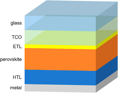
FIGURE 1. Simulated device architecture of a conventional (n-i-p) device used in this work. The layer thicknesses are chosen based on typical literature data as reported in Table 1.
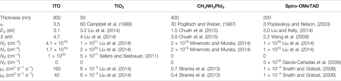
TABLE 1. Material and device parameters of the layers forming the generic PSC (n-i-p) as reported in Figure 1 εr is the relative permittivity, EG is the bandgap energy, Χ is the electron affinity, NC is the effective density of states of the conduction band, NV is the effective density of states of the valence band, ND the concentration of ionized donors, NA is the concentration of ionized acceptors, μn is the electron mobility and μp is the hole mobility.

TABLE 2. Parameters used for carrier recombination models.
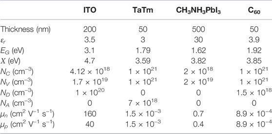
TABLE 3. Material and device parameters of the inverted PSC (p-i-n) with N4″-tetra([1,1′-biphenyl]-4-yl)-[1,1′:4′,1″-terphenyl]-4,4″-diamine (TaTm) as HTL and C60 as ETL [based on (Neukom, 2019)]
Modelling of Defects and Energy States
Ni et al. (2020) showed a clear decrease in defect density with the distance from the interface. Based on that insight, we use a novel approach to model the spatial distribution of defects. Figure 2 shows the spatial profile that we use in our simulations represented by an exponential function. Accordingly, defect densities are much higher at the perovskite interfaces adjacent to the transport layers and strongly decrease inside the absorber bulk, thus emulating the observations reported in (Ni et al., 2020). Penetration depths δETL and δHTL parametrize how far interface defects extend into the bulk. The defect density is given by:
where Nt, ETL and Nt, HTL are the defect densities at the ETL/perovskite and HTL/perovskite interfaces, xETL and xHTL are the positions of the respective interfaces and Nt,bulk is the bulk defect density. In conformity with the measurements from Ni et al. (2020), we assume that Nt, HTL and Nt, ETL are equal to 1018 cm−3 and 10−15 cm−3, respectively.

FIGURE 2. Spatial defect distribution used for the simulations in this work.
The energetic defect density profile is modelled using a Gaussian distribution.
Here Nt, 0 is the maximum defect density, Et,0 the average defect energy and ES the standard deviation of the Gaussian distribution. Evidence has been found for the existence of defects with transition energies around 0.15–0.30 eV (Duan et al., 2015; Heo et al., 2015). This simplified model is in agreement with a typical defect energy distribution as measured by Duan et al. (2015). In our simulations we used the parameters summarized in Table 4.
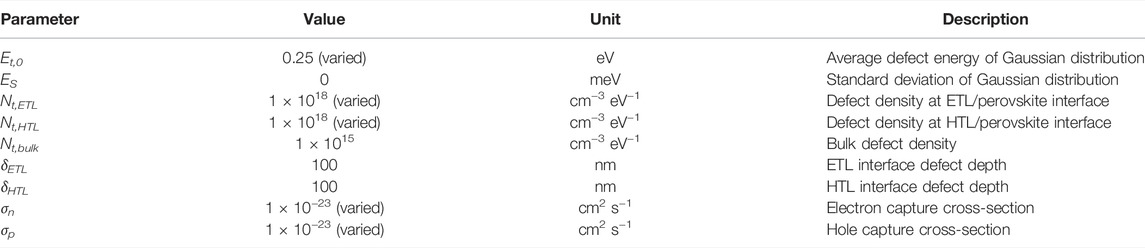
TABLE 4. Default parameters used within our analysis of the slow defects.
We consider double-state defects in the spatial and energy domain. In this work we focus on acceptor-like defects near the ETL and donor-like defects near the HTL, because we found that these energy states are active during the recombination processes in PSC simulations. It is worth mentioning that, in semiconductor materials, defects are commonly related to grain size and interface imperfections (Sze and Ng, 2006) and, in particular for PSC materials, defects can be ascribed to ions (Srivastava et al., 2020).
To quantify the magnitude of the hysteretic behaviour, we adopt the Hysteresis Index (HI) as defined by Nemnes et al. (2018), where the subscripts FS and RS indicate forward scan and reverse scan, respectively:
The Hysteresis Index is normalized, so that −1 < HI < 1. Larger (absolute) values of HI correspond to stronger hysteresis, with positive values corresponding to normal hysteresis and negative values corresponding to inverted hysteresis. In general, normal and inverted hysteresis indicate that J-V curves from reverse scan or forward scan cover higher J values in the voltage domain than in case of forward scan or reverse scan, respectively. For reference, HI = 0 indicates a PSC which is hysteresis-free.
Simulation Results
Hysteresis and Energy States
We first perform transient (time domain) simulations to evaluate the effect of the scan rate in a n-i-p device considering forward and reverse scan. Figure 3 shows simulated J-V curves of our reference n-i-p PSC under illumination for a range of scan rates between 0.01 and 1 V/s with their respective HI. We observe pronounced hysteresis (HI > 0.1) at scan rates in the range from 0.1 to 1 V/s. For slower scan rates hysteresis decreases, as both FS and RS approach the steady state J-V curve. In steady state the device is assumed to be in equilibrium, showing the long-term response of the system. The fact that in our simulations the steady-state J-V curve (dashed line in Figure 3) lies much lower than the J-V curves at high scan rates, reflects that the performance of the device degrades over a relatively short time (tens to hundreds of seconds). We observe a relatively low short circuit current due to the high interfacial defect densities that result in high recombination rates. On the contrary, for higher scan rates we observe reduced hysteresis, which goes along with improved performance. This reveals the complex process for device characterisation. In fact, the stable power conversion efficiency (as determined by the steady-state response) for this device cannot be accurately determined using scan rates higher than 0.01 V/s. The observed scan-rate dependency is in line with trends reported in literature (Snaith et al., 2014; Tress et al., 2015).
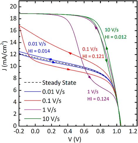
FIGURE 3. Simulated J-V curves under illumination for variable scan rates from 0.01 to 10 V/s. The calculated Hysteresis Indices are indicated next to each hysteretic path. Arrows denote the scan direction, while the dashed line represents the steady-state solution.
To analyse how interface defects near the ETL/perovskite interface influence hysteresis, cells with different values of peak of ETL defect density (Nt, ETL) were simulated. In Figure 4 the calculated Hysteresis Index is plotted as a function of scan rate for different Nt,ETL values. All the other parameters were kept constant as reported in Table 3. As expected, for low Nt, ETL (1 × 1018 cm−3) the HI exhibits the lowest values which stay below 0.03. By increasing the NT, ETL up to 5 × 1019 cm−3, the HI rapidly increases above 0.35. Due to the capacitive nature of photovoltaic devices, the HI is almost insensitive to the defect density for scan rates above 100 V/s. Indeed, HI variation is similar among Nt, ETL values scan rate >100 V/s. Note that HI increases for scan rate >100 V/s because of transition times between measurements are smaller than the time to fully arrange the charge inside the device to the voltage in stable conditions. This results in a measurement that depends on the previous condition of the device and increases HI.
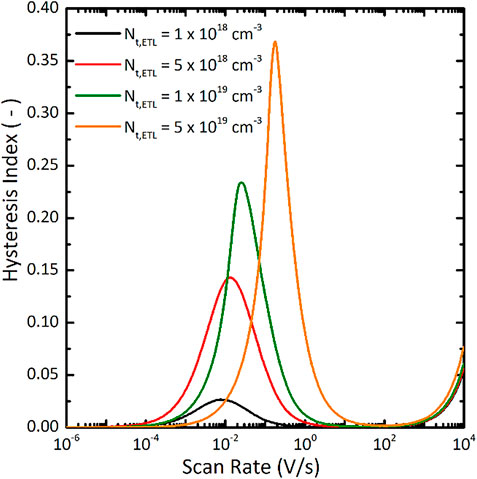
FIGURE 4. Distribution of hysteresis Indexes as function of the scan rate for PSCs simulated with variable defect density at the ETL/perovskite interface.
We found that the hysteresis directly correlates with the defect density at transport layer/perovskite interface. At this point, to study the effect of the energy of those defect states on the hysteresis, we simulated PSC’s featuring Et,0 ranging between 0.1 to 0.4 eV and 1.1–1.4 eV for defects close to ETL and HTL, respectively. Figure 5 shows the Hysteresis Index as a function of average defect energy for defects near the ETL (a) and defects near the HTL (b). For defects near the ETL, hysteresis is most apparent for Et,0 = 0.27 eV while for defects near the HTL the maximum occurs at Et, 0 = 1.26 eV. In general our simulations show that defects with energy close to the valence band quasi Fermi level (EF, p) or conduction band quasi Fermi level (EF, n) near the ETL and HTL, respectively, cause most severe hysteresis.
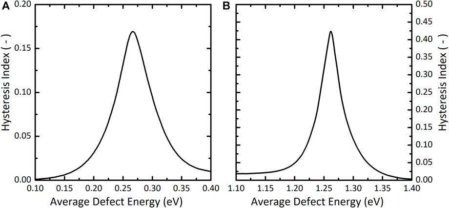
FIGURE 5. Hysteresis Index as a function of average defect energy Et,0 for a device with defects near the ETL (A) and defects near the HTL (B).
Besides studying the effect of Nt at the interface (see Figure 4ET,0 (see Figure 5) on the HI, we also analyse the effect of the capture cross-section (σ) of the defect states in the perovskite absorber bulk on the hysteresis. Figure 6 shows the HI as a function of scan rate for 3 cells with different capture cross-sections. The scan rate at which the HI is maximal decreases for lower capture cross-sections. In practice, hysteresis is observed for the commonly used range of 10−3 V s−1–100 V s−1 (Snaith et al., 2014; Tress et al., 2015). Our results show that σ thus should be lower than 10−23 cm2 to reproduce this behaviour. This value is extremely low compared to defects associated to other well-known semiconductor materials such as Si (Sze and Ng, 2006; Procel et al., 2020), SiO2 (Eades and Swanson, 1985) and GaAs (Lang and Logan, 1975).
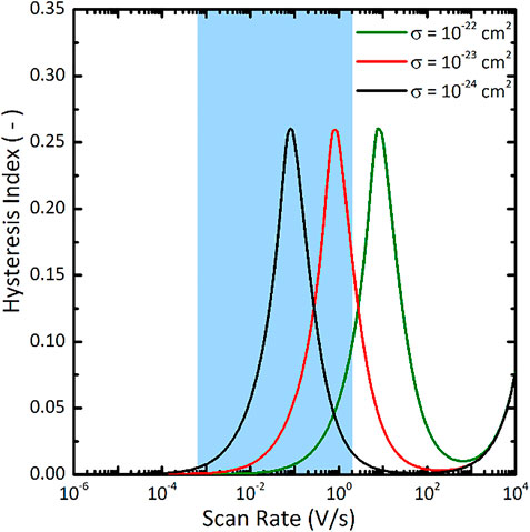
FIGURE 6. Hysteresis Index as a function of scan rate for devices simulated with varied capture cross-section defect states. The blue area denotes the range of scan rates for which maximal hysteresis is experimentally observed (Tress et al., 2015).
Moreover, the calculated σ based on the formula in ref. (Heiman and Warfield, 1965) and the experimental frequency response for ionic transport (τ−1 < 102 Hz) (Srivastava et al., 2020) is consistent with our findings reported in Figure 6 (σ < 10−22 cm2). This suggests that low σ can be correlated to ionic transport as discussed in ref. (Srivastava et al., 2020).
In fact, the frequency response of defect states (or alternately the capture and emission times) is proportional to the capture cross section (Sze and Ng, 2006). Therefore, we can relate the low capture cross sections with slow capture-emission processes.
Slow Dynamic Processes
Hysteresis in our simulated devices is attributable to slow capture and release of charge carriers by defects. The high amount of defect states near the interface gives rise to charge accumulation near the interface(s) and we can visualize that in Figure 7 for different voltage bias.
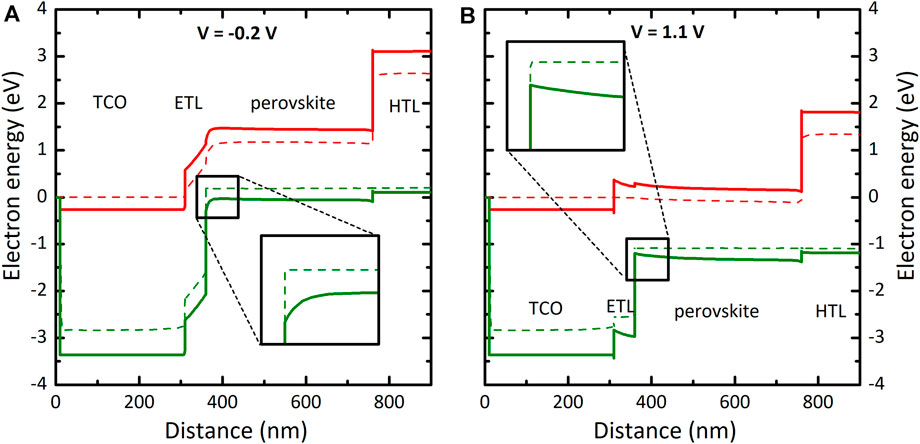
FIGURE 7. Band diagram in steady state when the device is (A) reverse biased (V = −0.2 V) and (B) forward biased (V = 1.1 V). The conduction band energy (CBE) and the valence band energy (VBE) are denoted with red and green lines, respectively. Dashed lines indicate the conduction band (green) and valence band (red) quasi-Fermi levels.
Figures 7A, B show the band diagram in steady state when the device is reverse biased (−0.2 V) and forward biased (1.1 V), respectively. We observe that near the ETL/perovskite interface EF, p is closer to the valence band energy (VBE) in forward bias than it is in reverse bias. Consequently, approaching the ETL interface, the concentration of holes (electrons) tends to be lower (higher) in reverse (forward) bias.
Indeed, in Figure 8, we observe the variation of concentration of electrons for different bias conditions: reverse bias (V = −0.2 V), forward bias (V = 1.1 V) and for two additional bias at V = 0.5 V and V = 0.8 V. There, we distinguish the steady state (dashed), forward scan (red) and reverse scan (blue) curves. Note that the scan starts at V = 1.1 V (blue curve in Figure 8D), switches scan direction at V = −0.2 V (blue and red curve in Figure 8A) and ends at V = 1.1 V (red curve in Figure 8D). The tendency of carrier trapping can be derived by taking the steady state profile as reference. That is, the transient profiles follow the steady-state profile: if the profile is below the steady state profile, the amount of trapped electrons tend to increase and if it is above the steady state profile, it tends to decrease.
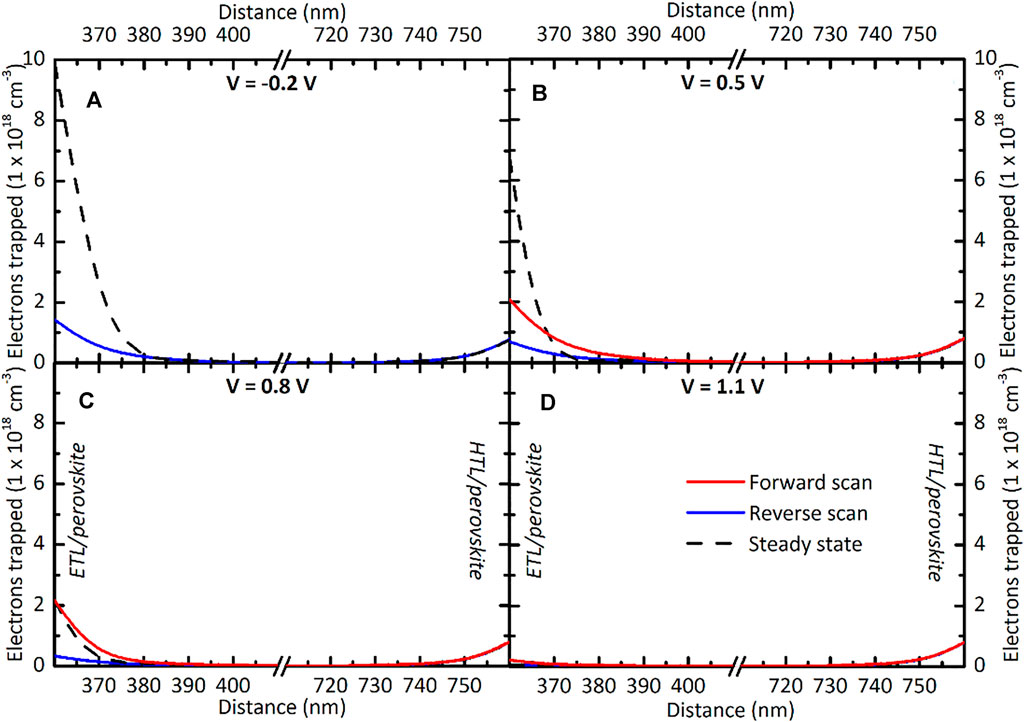
FIGURE 8. Depth profiles of trapped electrons in the perovskite layer as a function of position at different bias conditions: the ETL/perovskite interface is at the left side and the HTL/perovskite interface is at the right side. The red and blue lines denote the profiles during forward and reverse scan respectively. The steady state profile is indicated with a dashed line. Note that the horizontal axis is broken to highlight the differences near the interfaces. Simulations carried out at scan rate of 0.1 V/s.
Comparing Figure 8A and Figure 8D, we notice that much more charge is trapped in reverse bias (Figure 8A) near the ETL/perovskite interface. The lower concentration of holes (and higher concentration of electrons) causes a higher concentration of trapped electrons in reverse bias. Consequently, electrons must be released during the forward scan and captured during the reverse scan.
Because the processes of capture and emission are relatively slow compared to the scan rate, different profiles appear for the forward scan and reverse scan in Figure 8B and Figure 8C. During the reverse scan a relatively low amount of electrons is trapped because the capture process is incomplete and we assumed no trapped charge trapped as the initial conditions of our device (Figure 8D). On the other hand, during the forward scan the amount of electrons trapped is relatively high, as the process to release all the carriers that were trapped in reverse bias is incomplete (Figure 8A).
The higher concentration of trapped charge near the interface results in an electric field inside the absorber layer bulk that points in the direction of the ETL during the forward scan. Thus, during the forward scan, the trapped electrons effectively screen the internal electric field. To visualize that, we plot in Figure 9A the electron/hole densities profile inside the perovskite absorber layer for a constant voltage value of 0.8 V. We can observe that the collection of electrons is hindered and the total electron density inside the perovskite layer is significantly higher. A similar trend is found for the concentration of holes in the same Figure 9A where the hole density close to the ETL is significantly higher only in forward scan. The relatively high hole concentration close to ETL shields the electrons from flowing to the ETL. Both effects result in high recombination rates inside the bulk as shown in Figure 9B. Therefore, the forward scan displays a reduced output current compared to the reverse scan as we see in Figure 3.
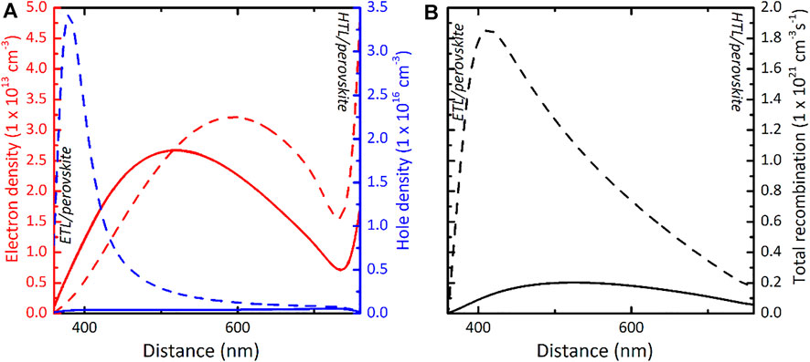
FIGURE 9. Depth profiles of (A) electron (red)/hole (blue) densities and (B) total recombination inside the perovskite absorber layer at an applied bias of 0.8 V. The ETL/perovskite interface is at the left side and the HTL/perovskite interface is at the right side. Each plot shows the profiles during the reverse scan (solid) and the forward scan (dashed). Simulations carried out at scan rate of 0.1 V/s.
Furthermore, looking back at Figure 4, the main reason for a higher HI at higher defect densities can be ascribed to the aforementioned charge accumulation and recombination (Sze and Ng, 2006). In fact, Shockley-Read-Hall recombination increases at higher defect densities that, together with the higher accumulation, results in a larger difference between the scan directions and thus stronger hysteresis in the J-V curve.
Energy States Contributing to Hysteresis
Our simulations reveal that recombination processes have a significant impact on hysteresis in PSCs. Such recombination processes are associated with the concentration and energy of energy states and their capture-emission properties (Sze and Ng, 2006). As we observe in Figure 5, only energy states in a certain energy range contribute to hysteresis. This can be explained by looking at their average occupation as shown in Figure 10 for electron and hole distributions as calculated in our simulated PSCs. The distributions depend on EF,p and EF,n. The electron distribution function determines the occupation of an electronic state. Note that the value of the electron distribution function equivalent to 1 as average occupation indicates that energy states are fully occupied by electrons.
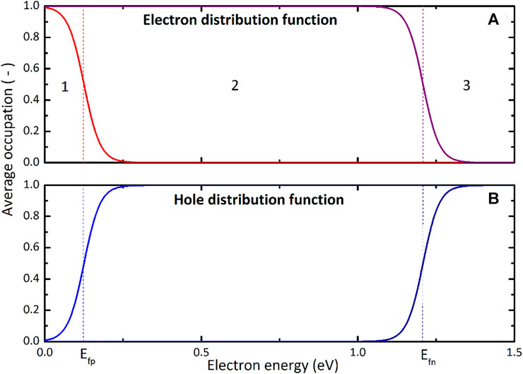
FIGURE 10. (A) Fermi-Dirac distribution function corresponding to the valence band (light red) and conduction band (dark red). (B) Distribution functions for holes, i.e. the complementary probability distributions of the Fermi-Dirac distributions in the top graph. The light blue curve corresponds to the valence band and the dark blue curve to the conduction band. Dashed lines indicate the quasi-Fermi levels. Recombination at ETL and HTL interfaces.
Defect states in regions 1 and 3 of Figure 10A cause hardly any hysteresis, because the number of trapped electrons in these states remains the same during the scan. They are either almost all occupied (region 1) or unoccupied (region 3). In region 2, however, there is a net emission of electrons to the valence band, but net capture of electrons from the conduction band. Which of two processes is dominant depends on the exact positions of the quasi Fermi-levels. Since the quasi Fermi-levels shift by a few tenths of an eV during a scan (see Figure 7), the amount of charge that is trapped close to the interface will strongly change during a scan. This build-up of charge is also clearly visible in Figure 8.
Figure 11 shows simulated J-V scans for the device architectures and defect distributions as summarized in Table 5. Figures 11A–C correspond to n-i-p architecture and Figure 11D represents a p-i-n structure. The simulated device in Figure 11A exhibits only acceptor like defects near the ETL with an average energy Et,0 = 0.25 eV. The device in Figure 11B exhibits only donor type defects near the HTL with an average energy Et, 0 = 1.3 eV. Hysteresis is more apparent in Figure 11B than in Figure 11A, showing a stronger “S-shaped” kink. Figure 11C reports the J-V scan of a device with defects near the ETL and defects near the HTL. This shows that hysteresis is even stronger if defects of both scenarios are present in the same device. In a way, the detrimental effect of charge polarisation on both sides of the perovskite layer adds up. Our model can be easily extended to other device architectures. For instance, Figure 12D shows the J-V curves we simulated for a p-i-n structure from Ref. (Neukom, 2019). Hysteresis is clearly present in the J-V curves and the forward scan has again a strong “S-shaped” kink.
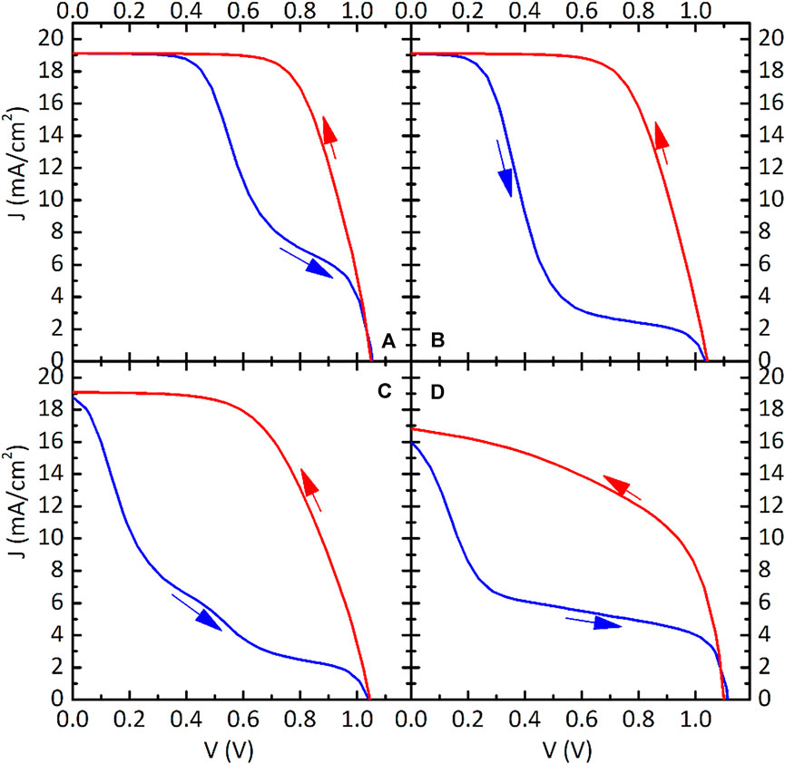
FIGURE 11. Simulated J-V scans for different device architectures and defect distributions. (A), (B) and (C) correspond to n-i-p structures whereas (D) to a p-i-n device. The properties are summarised in Table 5. The scan rate is kept constant at 0.1 V/s in all cases. The arrows indicates the scan direction.
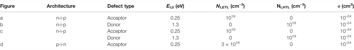
TABLE 5. Properties used for simulations of J-V curves in Figure 11.
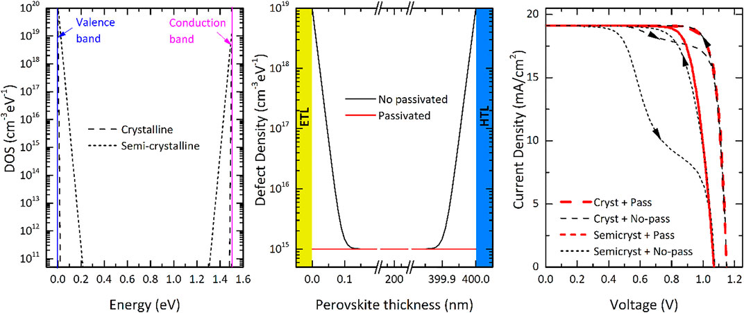
FIGURE 12. (A) Density of states as function of energy of two different perovskite materials (bandgap ∼1.5 eV) with different crystallinity fraction; (B) defect density across ETL/perovskite/HTL hetero-interfaces as function of perovskite thickness in case of (un-)passivated interfaces; (C) Current density—voltage characteristics of four modelled cases. The surface-passivated devices exhibit no hysteresis, while devices endowed with perovskite absorbers characterized by steep Urbach tails present higher open-circuit voltage (Voc).
Discussion
Looking at Figure 5, there are two energy ranges (around Et, 0 = 1.26 eV and Et,0 = 0.27 eV) in which electronic energy states would give rise to high HI’s. Both density-functional theory (DFT) calculations and measurements from literature indicate that real devices have indeed electronic energy states in these ranges. Duan et al. (2015) have identified the defect energy distribution which reveals a deep defect state at about 0.16 eV above the valence band in the MAPbI3 perovskite using admittance spectroscopy. Similarly, Xue et al. found hole traps using admittance spectroscopy in the energy range 0.16–0.23 eV with a relatively large concentration Nt = 1015–1016 cm−3 and a hole carrier capture cross-section in the range of 10−15–10−16 cm2s−1 (Xue et al., 2020). These defects were identified as interface-type defects. Measurements done by Heo et al. (2015) revealed defects with an higher activation energy of 0.27–0.28 eV and defect density of 1017 cm−3, slightly deeper than the aforementioned results. Shao et al. found even higher activation energies in the range of 0.35–0.40 eV. By means of photoluminescence measurements, the authors clearly verified that the majority of defect states are close to the surface of the MAPbI3 films and that they are most likely electron defects. Moreover, they were only able to passivate these defects by the diffusion of PCBM into the perovskite using thermal annealing. This experimental observation is in good agreement with our model representing defects that are not strictly localized at the interface, but that instead gradually fade away from the interface into the perovskite absorber.
The origin of those defect states is possibly attributed to the presence of interstitial iodine. According to DFT calculations, an acceptor-like defect with ET = 0.18 eV above the valence band edge is introduced by such defects (Du, 2014). The interstitial iodine is the only one among the native defects (i.e., vacancies, interstitials, and antisites) causing a low-energy defect state (Ball and Petrozza, 2016). Moreover, Mosconi et al. (2016) found defects related to iodine with characteristic energy of 0.15 eV above the valence band. DFT analysis of surface defects showed that only iodine interstitial has a deep carrier-trapping state (Uratani and Yamashita, 2017). Hence, the hysteresis might be related to the slow movement and recombination of carriers through energy states linked to ionized molecules.
These insights are crucial for the development of high-efficiency and hysteresis-free PSCs. In our simulation platform we are able to evaluate the crystallinity of the perovskite in terms of characteristic energy of the band tail states (Urbach energy). Accordingly, higher values of characteristic energy correspond to amorphous structures while minimal values to crystalline structures (Wager, 2017). Similarly, the quality of the passivation is considered in terms of NT,ETL and NT,HTL. We observe in Figure 12 that high quality (= high crystallinity) perovskite material increases the device open-circuit voltage. However we find that solely improving the perovskite material or the surface passivation is not sufficient to eliminate the hysteresis. Only the concurrent implementation of both high quality perovskite material and surface passivation can yield highest efficiency with negligible hysteresis.
It should be noted that our results do not reproduce different open-circuit voltage (Voc) values as some experimental J-V curves do. This was also noted by van Reenen et al. when they modeled hysteresis using ion migration (van Reenen et al., 2015). Further research is needed in order to explain the mechanisms leading to Voc mismatch during hysteresis in perovskite solar cells.
It is often suggested that ion migration is a primary cause of hysteresis. The hypothesis is that slowly excess ions are present in the perovskite crystal, that slowly move through the perovskite bulk and accumulate at the interfaces under short circuit conditions (Snaith et al., 2014). In fact, perovskites exhibit high ionic conductivity caused by the migration of halide-ions (Mizusaki et al., 1983) but observed ion migration lengths are only 1/3 of a common perovskite layer thickness (110–130 nm) (Lee et al., 2017). Additionally, hysteresis has been successfully emulated using mobile ions (van Reenen et al., 2015; Walter et al., 2018), but it strongly depends on the surface recombination at perovskite/HTL and/ETL interfaces (Neukom et al., 2017; Neukom, 2019). This suggests that hysteresis can be reduced by changing the interfacial contact materials and thus reducing recombination mechanisms at the interfaces (Calado et al., 2016). Nevertheless, to elucidate the role of ion migration, it is important to obtain a better understanding of possible mechanisms like chemical binding or complexation at the interfaces (Weber et al., 2018). The simulations described in this work reveal that hysteresis in perovskite solar cells can be mimicked by explicitly modelling shadow interface defects. Our simulation results are consistent with the fact that surface passivation can be used to eliminate hysteresis (Shao et al., 2014; Wojciechowski et al., 2014; Jiang et al., 2019). Moreover, several works reported experimental and theoretical evidence for shallow defect states in perovskites (Yin et al., 2014a; Yin et al., 2014b; Baumann et al., 2015; Shi et al., 2015; Wright et al., 2017; Ni et al., 2020). In this respect, further empirical research is needed to characterize the capture-emission times of shallow defects. All aspects considered, additional modeling studies could help to improve our understanding about the combined effect of ion migration and slow recombination processes, as well as the implications of limited ion migration lengths.
Conclusion
In this work we have explained the hysteretic behaviour of PSCs in terms of charge carrier accumulation due to energy states near the interfaces with the perovskite absorber. Such phenomena were modelled using fundamental semiconductor physics equations numerically solved in the finite element simulator TCAD Sentaurus.
Our simulations revealed that hysteretic behaviour can be caused by defects near the interface with ETL (or HTL) with the following characteristics: 1) density Nt > 1018 cm−3 2) capture cross-section σ ≈ 10−23 cm2, and 3) defect energy Et ≈ 0.25 eV with respect to VBE (or Et ≈ 0.2 eV with respect to CBE). Such values are consistent with experimental findings reported in literature.
Furthermore, stronger hysteresis at higher defect densities near the ETL or HTL revealed that the hysteretic behaviour is due to recombination processes. We provided an explanation of the observed phenomena in terms of slow capture and emission by interface defect states with capture cross-sections lower than 10−22 cm2. Moreover, the effect is most apparent when the energy states have energies close to the quasi-Fermi levels.
Finally, J-V simulations at different scan rates demonstrated realistic behaviour in the analysis of hysteresis for different scan rates. In fact, we found that there is a scan rate which maximizes hysteresis as observed in experimental studies.
In conclusion, our results show that hysteresis can be explained using fundamental semiconductor physics alone with realistic defect distributions in both the spatial and energetic domains. This supports the claim that interface defects play a crucial role in the formation of hysteresis. At the same time, we observe that independently improving perovskite material or quenching interface defects is not sufficient to eliminate the hysteresis. Rather, only concurrently pursuing high quality perovskite material and surface passivation yields highest efficiency with negligible hysteresis. Our model can be easily extended and adapted to different device architectures and defect distributions for a custom optimization that addresses different fabrication sequence, absorber material formulations and choice of supporting layers.
Data Availability Statement
The raw data supporting the conclusion of this article will be made available by the authors, without undue reservation.
Author Contributions
RH and PP conceived the idea. RH designed the simulation template. LM, RS, and OI contributed to the definition and presentation of the paper content. RH, PP, LM, RS, and OI discussed the results. RH, PP, and OI organized the research. RH wrote the paper, and all other authors provided feedback.
Conflict of Interest
The authors declare that the research was conducted in the absence of any commercial or financial relationships that could be construed as a potential conflict of interest.
Publisher’s Note
All claims expressed in this article are solely those of the authors and do not necessarily represent those of their affiliated organizations, or those of the publisher, the editors and the reviewers. Any product that may be evaluated in this article, or claim that may be made by its manufacturer, is not guaranteed or endorsed by the publisher.
References
Al-Ashouri, A., Köhnen, E., Li, B., Magomedov, A., Hempel, H., Caprioglio, P., et al. (2020). Monolithic Perovskite/Silicon Tandem Solar Cell with >29% Efficiency by Enhanced Hole Extraction. Science 370 (6522), 1300–1309. doi:10.1126/science.abd4016
Almansouri, I., Ho-Baillie, A., Bremner, S. P., and Green, M. A. (2015). Supercharging Silicon Solar Cell Performance by Means of Multijunction Concept. IEEE J. Photovoltaics 5 (3), 968–976. doi:10.1109/jphotov.2015.2395140
Almora, O., Zarazua, I., Mas-Marza, E., Mora-Sero, I., Bisquert, J., and Garcia-Belmonte, G. (2015). Capacitive Dark Currents, Hysteresis, and Electrode Polarization in Lead Halide Perovskite Solar Cells. J. Phys. Chem. Lett. 6 (9), 1645–1652. doi:10.1021/acs.jpclett.5b00480
Ball, J. M., and Petrozza, A. (2016). Defects in Perovskite-Halides and Their Effects in Solar Cells. Nat. Energy 1 (11), 16149. doi:10.1038/nenergy.2016.149
Baumann, A., Väth, S., Rieder, P., Heiber, M. C., Tvingstedt, K., and Dyakonov, V. (2015). Identification of Trap States in Perovskite Solar Cells. J. Phys. Chem. Lett. 6 (12), 2350–2354. doi:10.1021/acs.jpclett.5b00953
Calado, P., Telford, A. M., Bryant, D., Li, X., Nelson, J., O'Regan, B. C., et al. (2016). Evidence for Ion Migration in Hybrid Perovskite Solar Cells with Minimal Hysteresis. Nat. Commun. 7 (1), 13831–13910. doi:10.1038/ncomms13831
Campbell, S. A., Kim, H.-S., Gilmer, D. C., He, B., Ma, T., and Gladfelter, W. L. (1999). Titanium Dioxide (TiO2)-Based Gate Insulators. IBM J. Res. Dev. 43 (3), 383–392. doi:10.1147/rd.433.0383
Chueh, C.-C., Li, C.-Z., and Jen, A. K.-Y. (2015). Recent Progress and Perspective in Solution-Processed Interfacial Materials for Efficient and Stable Polymer and Organometal Perovskite Solar Cells. Energy Environ. Sci. 8 (4), 1160–1189. doi:10.1039/c4ee03824j
Das, B., Aguilera, I., Rau, U., and Kirchartz, T. (2020). What Is a Deep Defect? Combining Shockley-Read-Hall Statistics with Multiphonon Recombination Theory. Phys. Rev. Mater. 4 (2), 24602. doi:10.1103/physrevmaterials.4.024602
Du, M. H. (2014). Efficient Carrier Transport in Halide Perovskites: Theoretical Perspectives. J. Mat. Chem. A 2 (24), 9091–9098. doi:10.1039/c4ta01198h
Duan, H.-S., Zhou, H., Chen, Q., Sun, P., Luo, S., Song, T.-B., et al. (2015). The Identification and Characterization of Defect States in Hybrid Organic-Inorganic Perovskite Photovoltaics. Phys. Chem. Chem. Phys. 17 (1), 112–116. doi:10.1039/c4cp04479g
Eades, W. D., and Swanson, R. M. (1985). Calculation of Surface Generation and Recombination Velocities at the Si‐SiO2interface. J. Appl. Phys. 58 (11), 4267–4276. doi:10.1063/1.335562
Elumalai, N. K., and Uddin, A. (2016). Hysteresis in Organic-Inorganic Hybrid Perovskite Solar Cells. Sol. Energy Mater. Sol. Cells 157, 476–509. doi:10.1016/j.solmat.2016.06.025
García-Cañadas, J., Fabregat-Santiago, F., Bolink, H. J., Palomares, E., Garcia-Belmonte, G., and Bisquert, J. (2006). Determination of Electron and Hole Energy Levels in Mesoporous Nanocrystalline TiO2 Solid-State Dye Solar Cell. Synth. Metall. 156 (14–15), 944–948. doi:10.1016/j.synthmet.2006.06.006
Green, M. A., Dunlop, E. D., Hohl‐Ebinger, J., Yoshita, M., Kopidakis, N., and Hao, X. (2020). Solar Cell Efficiency Tables (Version 56). Prog. Photovolt. Res. Appl. 28 (7), 629–638. doi:10.1002/pip.3303
Green, M. A., Ho-Baillie, A., and Snaith, H. J. (2014). The Emergence of Perovskite Solar Cells. Nat. Phot. 8 (7), 506–514. doi:10.1038/nphoton.2014.134
Heiman, F. P., and Warfield, G. (1965). The Effects of Oxide Traps on the MOS Capacitance. IEEE Trans. Electron Devices 12 (4), 167–178. doi:10.1109/t-ed.1965.15475
Heo, J. H., Song, D. H., Han, H. J., Kim, S. Y., Kim, J. H., Kim, D., et al. (2015). Planar CH3NH3PbI3 Perovskite Solar Cells with Constant 17.2% Average Power Conversion Efficiency Irrespective of the Scan Rate. Adv. Mat. 27 (22), 3424–3430. doi:10.1002/adma.201500048
Hörantner, M. T., Ziffe, M., and Eperon, G. E. (2017). The Potential of Multijunction Perovskite Solar Cells. ACS Energy Lett. 2 (10), 2506–2513.
Ji, K., Anaya, M., Abfalterer, A., and Stranks, S. D. (2021). Halide Perovskite Light‐Emitting Diode Technologies. Adv. Opt. Mat. 9 (18), 2002128.
Jiang, Q., Zhao, Y., Zhang, X., Yang, X., Chen, Y., Chu, Z., et al. (2019). Surface Passivation of Perovskite Film for Efficient Solar Cells. Nat. Photonics 13 (7), 460–466. doi:10.1038/s41566-019-0398-2
Kojima, A., Teshima, K., Shirai, Y., and Miyasaka, T. (2009). Organometal Halide Perovskites as Visible-Light Sensitizers for Photovoltaic Cells. J. Am. Chem. Soc. 131 (17), 6050–6051. doi:10.1021/ja809598r
Lal, N. N., Dkhissi, Y., Li, W., Hou, Q., Cheng, Y.-B., and Bach, U. (2017). Perovskite Tandem Solar Cells. Adv. Energy Mat. 7 (18), 16. doi:10.1002/aenm.201602761
Lang, D. V., and Logan, R. A. (1975). A Study of Deep Levels in GaAs by Capacitance Spectroscopy. J. Electron. Mater. 4 (5), 1053–1066. doi:10.1007/bf02660189
Lee, H., Gaiaschi, S., Chapon, P., Marronnier, A., Lee, H., Vanel, J.-C., et al. (2017). Direct Experimental Evidence of Halide Ionic Migration Under Bias in CH3NH3PbI3-xClx-Based Perovskite Solar Cells Using GD-OES Analysis. ACS Energy Lett. 2 (4), 943–949. doi:10.1021/acsenergylett.7b00150
Li, C., Wang, H., Wang, F., Li, T., Xu, M., Wang, H., et al. (2020). Ultrafast and Broadband Photodetectors Based on a Perovskite/organic Bulk Heterojunction for Large-Dynamic-Range Imaging. Light Sci. Appl. 9 (1), 31. doi:10.1038/s41377-020-0264-5
Li, H., and Zhang, W. (2020). Perovskite Tandem Solar Cells: From Fundamentals to Commercial Deployment. Chem. Rev. 120 (18), 9835–9950. doi:10.1021/acs.chemrev.9b00780
Li, Z. (2019). A Generic Green Solvent Concept Boosting the Power Conversion Efficiency of All-Polymer Solar Cells to 11. Energy and Environ. Sci. 12 (1), 157–163.
Lin, R. (2019). Monolithic All-Perovskite Tandem Solar Cells with 24.8\% Efficiency Exploiting Comproportionation to Suppress Sn (Ii) Oxidation in Precursor Ink. Nat. Energy 4 (10), 864–873.
Liu, D., and Kelly, T. L. (2014). Perovskite Solar Cells with a Planar Heterojunction Structure Prepared Using Room-Temperature Solution Processing Techniques. Nat. Phot. 8 (2), 133–138. doi:10.1038/nphoton.2013.342
Liu, F., Zhu, J., Wei, J., Li, Y., Lv, M., Yang, S., et al. (2014). Numerical Simulation: toward the Design of High-Efficiency Planar Perovskite Solar Cells. Appl. Phys. Lett. 104 (25), 253508. doi:10.1063/1.4885367
Miao, J., and Zhang, F. (2019). Recent Progress on Highly Sensitive Perovskite Photodetectors. J. Mat. Chem. C 7 (7), 1741–1791. doi:10.1039/c8tc06089d
Minemoto, T., and Murata, M. (2014). Device Modeling of Perovskite Solar Cells Based on Structural Similarity with Thin Film Inorganic Semiconductor Solar Cells. J. Appl. Phys. 116 (5), 54505. doi:10.1063/1.4891982
Mizusaki, J., Arai, K., and Fueki, K. (1983). Ionic Conduction of the Perovskite-type Halides. Solid State Ionics 11 (3), 203–211. doi:10.1016/0167-2738(83)90025-5
Mosconi, E., Meggiolaro, D., Snaith, H. J., Stranks, S. D., and De Angelis, F. (2016). Light-induced Annihilation of Frenkel Defects in Organo-Lead Halide Perovskites. Energy Environ. Sci. 9 (10), 3180–3187. doi:10.1039/c6ee01504b
Nature Energy (2020). Perovskites Take Steps to Industrialization, Nat. Energy 5 (1). doi:10.1038/s41560-020-0552-6
Nemnes, G. A., Besleaga, C., Tomulescu, A. G., Palici, A., Pintilie, L., Manolescu, A., et al. (2018). How Measurement Protocols Influence the Dynamic J-V Characteristics of Perovskite Solar Cells: Theory and Experiment. Sol. Energy 173, 976–983. doi:10.1016/j.solener.2018.08.033
Neukom, M. T. (2019). Consistent Device Simulation Model Describing Perovskite Solar Cells in Steady-State, Transient and Frequency Domain. ACS Appl. Mat. \& interfaces. doi:10.1021/acsami.9b04991
Neukom, M. T., Züfle, S., Knapp, E., Makha, M., Hany, R., and Ruhstaller, B. (2017). Why Perovskite Solar Cells with High Efficiency Show Small IV-Curve Hysteresis. Sol. Energy Mater. Sol. Cells 169, 159–166. doi:10.1016/j.solmat.2017.05.021
Ni, Z., Bao, C., Liu, Y., Jiang, Q., Wu, W. Q., Chen, S., et al. (2020). Resolving Spatial and Energetic Distributions of Trap States in Metal Halide Perovskite Solar Cells. Science 367 (6484), 1352–1358. doi:10.1126/science.aba0893
Poglitsch, A., and Weber, D. (1987). Dynamic Disorder in Methylammoniumtrihalogenoplumbates (II) Observed by Millimeter‐Wave Spectroscopy. J. Chem. Phys. 87 (11), 6373–6378. doi:10.1063/1.453467
Poplavskyy, D., and Nelson, J. (2003). Nondispersive Hole Transport in Amorphous Films of Methoxy-Spirofluorene-Arylamine Organic Compound. J. Appl. Phys. 93 (1), 341–346. doi:10.1063/1.1525866
Procel, P., Xu, H., Saez, A., Ruiz‐Tobon, C., Mazzarella, L., Zhao, Y., et al. (2020). The Role of Heterointerfaces and Subgap Energy States on Transport Mechanisms in Silicon Heterojunction Solar Cells. Prog. Photovolt. Res. Appl. 28 (9), 935–945. doi:10.1002/pip.3300
Rong, Y., Hu, Y., Ravishankar, S., Liu, H., Hou, X., Sheng, Y., et al. (2017). Tunable Hysteresis Effect for Perovskite Solar Cells. Energy Environ. Sci. 10 (11), 2383–2391. doi:10.1039/c7ee02048a
Sanchez, R. S., Gonzalez-Pedro, V., Lee, J.-W., Park, N.-G., Kang, Y. S., Mora-Sero, I., et al. (2014). Slow Dynamic Processes in Lead Halide Perovskite Solar Cells. Characteristic Times and Hysteresis. J. Phys. Chem. Lett. 5 (13), 2357–2363. doi:10.1021/jz5011187
Sellers, M. C. K., and Seebauer, E. G. (2011). Manipulation of Polycrystalline TiO2 Carrier Concentration via Electrically Active Native Defects. J. Vac. Sci. \& Technol. A Vac. Surfaces, Film. 29 (6), 61503. doi:10.1116/1.3635373
Shao, Y., Xiao, Z., Bi, C., Yuan, Y., and Huang, J. (2014). Origin and Elimination of Photocurrent Hysteresis by Fullerene Passivation in CH3NH3PbI3 Planar Heterojunction Solar Cells. Nat. Commun. 5 (1), 5784. doi:10.1038/ncomms6784
Shi, D., Adinolfi, V., Comin, R., Yuan, M., Alarousu, E., Buin, A., et al. (2015). Low Trap-State Density and Long Carrier Diffusion in Organolead Trihalide Perovskite Single Crystals. Science 347 (6221), 519–522. doi:10.1126/science.aaa2725
Snaith, H. J., Abate, A., Ball, J. M., Eperon, G. E., Leijtens, T., Noel, N. K., et al. (2014). Anomalous Hysteresis in Perovskite Solar Cells. J. Phys. Chem. Lett. 5 (9), 1511–1515. doi:10.1021/jz500113x
Snaith, H. J., and Grätzel, M. (2006). Enhanced Charge Mobility in a Molecular Hole Transporter via Addition of Redox Inactive Ionic Dopant: Implication to Dye-Sensitized Solar Cells. Appl. Phys. Lett. 89 (26), 262114. doi:10.1063/1.2424552
Srivastava, P., Kumar, R., and Bag, M. (2020). Discerning the Role of an A-Site Cation and X-Site Anion for Ion Conductivity Tuning in Hybrid Perovskites by Photoelectrochemical Impedance Spectroscopy. J. Phys. Chem. C 125 (1), 211–222. doi:10.1021/acs.jpcc.0c09443
Stranks, S. D., Eperon, G. E., Grancini, G., Menelaou, C., Alcocer, M. J. P., Leijtens, T., et al. (2013). Electron-hole Diffusion Lengths Exceeding 1 Micrometer in an Organometal Trihalide Perovskite Absorber. Science 342 (6156), 341–344. doi:10.1126/science.1243982
Synopsys, I. (2015). Sentaurus Device User Guide Version K-2015.06. Mountain View, CA, USA: Synopsys.
Sze, S. M., and Ng, K. K. (2006). Physics of Semiconductor Devices. Third. Hoboken, NJ, USA: John Wiley & Sons.
Tan, Z.-K., Moghaddam, R. S., Lai, M. L., Docampo, P., Higler, R., Deschler, F., et al. (2014). Bright Light-Emitting Diodes Based on Organometal Halide Perovskite. Nat. Nanotech 9 (9), 687–692. doi:10.1038/nnano.2014.149
Tao, S., Schmidt, I., Brocks, G., Jiang, J., Tranca, I., Meerholz, K., et al. (2019). Absolute Energy Level Positions in Tin- and Lead-Based Halide Perovskites. Nat. Commun. 10 (1), 2560. doi:10.1038/s41467-019-10468-7
Tonui, P., Oseni, S. O., Sharma, G., Yan, Q., and Tessema Mola, G. (2018). Perovskites Photovoltaic Solar Cells: An Overview of Current Status. Renew. Sustain. Energy Rev. 91, 1025–1044. doi:10.1016/j.rser.2018.04.069
Tress, W., Marinova, N., Moehl, T., Zakeeruddin, S. M., Nazeeruddin, M. K., and Grätzel, M. (2015). Understanding the Rate-Dependent J-V Hysteresis, Slow Time Component, and Aging in CH3NH3PbI3 Perovskite Solar Cells: the Role of a Compensated Electric Field. Energy Environ. Sci. 8 (3), 995–1004. doi:10.1039/c4ee03664f
Unger, E. L., Hoke, E. T., Bailie, C. D., Nguyen, W. H., Bowring, A. R., Heumüller, T., et al. (2014). Hysteresis and Transient Behavior in Current-Voltage Measurements of Hybrid-Perovskite Absorber Solar Cells. Energy Environ. Sci. 7 (11), 3690–3698. doi:10.1039/c4ee02465f
Uratani, H., and Yamashita, K. (2017). Charge Carrier Trapping at Surface Defects of Perovskite Solar Cell Absorbers: a First-Principles Study. J. Phys. Chem. Lett. 8 (4), 742–746. doi:10.1021/acs.jpclett.7b00055
van Reenen, S., Kemerink, M., and Snaith, H. J. (2015). Modeling Anomalous Hysteresis in Perovskite Solar Cells. J. Phys. Chem. Lett. 6 (19), 3808–3814. doi:10.1021/acs.jpclett.5b01645
Vdma, International. (2021). Technology Roadmap for Photovoltaic. Frankfurt am Main, Germany: ITRPV.
Wager, J. F. (2017). Real- and Reciprocal-Space Attributes of Band Tail States. AIP Adv. 7 (12), 125321. doi:10.1063/1.5008521
Walter, D., Fell, A., Wu, Y., Duong, T., Barugkin, C., Wu, N., et al. (2018). Transient Photovoltage in Perovskite Solar Cells: Interaction of Trap-Mediated Recombination and Migration of Multiple Ionic Species. J. Phys. Chem. C 122 (21), 11270–11281. doi:10.1021/acs.jpcc.8b02529
Wang, M., Grätzel, C., Moon, S.-J., Humphry-Baker, R., Rossier-Iten, N., Zakeeruddin, S. M., et al. (2009). Surface Design in Solid-State Dye Sensitized Solar Cells: Effects of Zwitterionic Co-adsorbents on Photovoltaic Performance. Adv. Funct. Mat. 19 (13), 2163–2172. doi:10.1002/adfm.200900246
Weber, S. A. L., Hermes, I. M., Turren-Cruz, S.-H., Gort, C., Bergmann, V. W., Gilson, L., et al. (2018). How the Formation of Interfacial Charge Causes Hysteresis in Perovskite Solar Cells. Energy Environ. Sci. 11 (9), 2404–2413. doi:10.1039/c8ee01447g
Wojciechowski, K., Stranks, S. D., Abate, A., Sadoughi, G., Sadhanala, A., Kopidakis, N., et al. (2014). Heterojunction Modification for Highly Efficient Organic-Inorganic Perovskite Solar Cells. ACS Nano 8 (12), 12701–12709. doi:10.1021/nn505723h
Wright, A. D., Milot, R. L., Eperon, G. E., Snaith, H. J., Johnston, M. B., and Herz, L. M. (2017). Band-Tail Recombination in Hybrid Lead Iodide Perovskite. Adv. Funct. Mat. 27 (29), 1700860. doi:10.1002/adfm.201700860
Wu, Y., Shen, H., Walter, D., Jacobs, D., Duong, T., Peng, J., et al. (2016). On the Origin of Hysteresis in Perovskite Solar Cells. Adv. Funct. Mat. 26 (37), 6807–6813. doi:10.1002/adfm.201602231
Xiao, K. (2020a). All-perovskite Tandem Solar Cells with 24.2% Certified Efficiency and Area over 1 Cm2 Using Surface-Anchoring Zwitterionic Antioxidant. Nat. Energy 5 (11), 870–880.
Xiao, K. (2020b). Solution-Processed Monolithic All-Perovskite Triple-Junction Solar Cells with Efficiency Exceeding 20. ACS Energy Lett. 5 (9), 2819–2826.
Xue, J., Hu, X., Guo, Y., Weng, G., Jiang, J., Chen, S., et al. (2020). Diagnosis of Electrically Active Defects in CH3NH3PbI3 Perovskite Solar Cells via Admittance Spectroscopy Measurements. Appl. Opt. 59 (2), 552–557. doi:10.1364/ao.59.000552
Yan, J., Savenije, T. J., Mazzarella, L., and Isabella, O. (2022). Progress and Challenges on Scaling up of Perovskite Solar Cell Technology. Sustain. Energy Fuels 6 (2), 243–266. doi:10.1039/d1se01045j
Yin, W.-J., Shi, T., and Yan, Y. (2014a). Unusual Defect Physics in CH3NH3PbI3 Perovskite Solar Cell Absorber. Appl. Phys. Lett. 104 (6), 63903. doi:10.1063/1.4864778
Yin, W.-J., Shi, T., and Yan, Y. (2014b). Unique Properties of Halide Perovskites as Possible Origins of the Superior Solar Cell Performance. Adv. Mat. 26 (27), 4653–4658. doi:10.1002/adma.201306281
Keywords: TCAD senaturus, hysteresis, perovskite solar cell device simulation, defect states simulations, defect distribution model
Citation: van Heerden R, Procel P, Mazzarella L, Santbergen R and Isabella O (2022) Slow Shallow Energy States as the Origin of Hysteresis in Perovskite Solar Cells. Front. Photonics 3:889837. doi: 10.3389/fphot.2022.889837
Received: 04 March 2022; Accepted: 13 April 2022;
Published: 18 May 2022.
Edited by:
Jianyu Yuan, Soochow University, ChinaReviewed by:
Klaus Weber, Australian National University, AustraliaYao Wang, Shanghai Jiao Tong University, China
Copyright © 2022 van Heerden, Procel, Mazzarella, Santbergen and Isabella. This is an open-access article distributed under the terms of the Creative Commons Attribution License (CC BY). The use, distribution or reproduction in other forums is permitted, provided the original author(s) and the copyright owner(s) are credited and that the original publication in this journal is cited, in accordance with accepted academic practice. No use, distribution or reproduction is permitted which does not comply with these terms.
*Correspondence: Paul Procel, cC5hLnByb2NlbG1veWFAdHVkZWxmdC5ubA==