
94% of researchers rate our articles as excellent or good
Learn more about the work of our research integrity team to safeguard the quality of each article we publish.
Find out more
ORIGINAL RESEARCH article
Front. Nucl. Eng., 16 November 2022
Sec. Nuclear Materials
Volume 1 - 2022 | https://doi.org/10.3389/fnuen.2022.1034114
This article is part of the Research TopicAdvancements in Nuclear and Irradiation ExperimentsView all 6 articles
 H. A. A. Abdelbagi1,2*
 T. A. O. Jafer1V. A. Skuratov3,4E. G. Njoroge1,5M. Mlambo1,6T. T. Hlatshwayo1J. B. Malherbe1†
Polycrystalline SiC wafers were implanted with 360 keV strontium (Sr) ions at room temperature (RT)to a fluence of 2 × 1016 cm−2. Some of the implanted samples were irradiated with xenon (Xe) ions of 167 MeV to a fluence of 3.4 × 1014 cm−2 and 8.4 × 1014 cm−2at RT. The as-implanted and implanted then irradiated samples were vacuum annealed (isochronally) at temperatures ranging from 1,100 to 1,400°C in steps of 100°C for 5 h. Annealing induced modification of the microstructure of the implanted and swift heavy ions (SHIs) irradiated SiC was studied by Raman spectroscopy, scanning electron microscopy (SEM) and backscattering spectrometry (RBS). Sr ions bombardment caused formation of an amorphous layer in SiC, while irradiation by Xe ions led to partial recrystallization of the amorphized layer. After annealing at 1,100°C, the samples with low Sr retained ratio showed full recrystallization, while the samples with high Sr retained ratio showed poor recrystallization. This suggests that the presence of Sr within the implanted region inhibited the recrystallization of SiC. Annealing of the as-implanted samples at temperatures from 1,100°C and 1,200°Cresulted in larger average crystal size compared to the SHIsirradiated samples annealed in the same temperature range. The difference in the average crystal sizes between the as-implanted and SHIs irradiated samples was due to the differences in the nucleation rate per amorphous area in the two samples. Ramanspectroscopy results showedthat the intensity of the LO mode of SiC increases with increasing crystal size. However, several factors such as pores and defects in SiC play a role in the decrease of the LO mode intensity of SiC (even if the average crystal size is large).
Due to its outstanding properties which includesresistance to chemical attacks (Gurban et al., 2015), highthermal conductivity, radiation resistance against neutron bombardment (Malherbe, 2013), high hardness (Goldberg et al., 2001) and low neutron cross section, SiC is used as the main barrier to fission products release in tri-structural isotropic (TRISO) particle fuelin thepebble bed modular reactor (PBMR) (Verfondern et al., 2007; Malherbe et al., 2008; Petti et al., 2012; Malherbe, 2013). The TRISO particle was designed to keep the fission products within the particle during the normal nuclear reactor operation and under reactor accident conditions. However, some of the solid and gaseous fission products [such assilver (Ag), caesium (Cs), strontium (Sr), krypton (Kr) and xenon (Xe)] have been detected outside the TRISO particle at temperatures higher than 1,000°C (TECDOC- 978, 1997). The release of the radioactive fission products (such as Sr) from the reactor can pose radiological health concerns (Friedland et al., 2012). The radioactive isotope of Sr has a chemical similarity to calcium, which causes Sr to be deposited in bones. This makes strontium a key fission product and its transport property in the TRISO particle needs to be investigated. Since SiC is the main fission products diffusion barrier in TRISO particle, it is important to study the mechanisms of the migration behaviour of Sr in SiC. Therefore, several studies have been carried out (such as a multi-layer diffusion couple (Dwaraknath and Was, 2014), and ion implantation to investigate Sr behavior in SiC at very high temperatures (Friedland et al., 2012; Dwaraknath and Was, 2016; Abdelbagi et al., 2019a; Hlatshwayo et al., 2020)) to understand the transport mechanism of Sr through the SiC layer. In our previous study, we found that the swift heavy ion irradiation (SHIs) enhances the diffusion of implanted Sr in SiC (Abdelbagi et al., 2019a). The results indicated that this was due to the differences in the microstructure between the SHIs irradiated and as-implanted samples.
The SiC microstructure (such as crystal structures, orientations and sizes) can play a significant role in the diffusion of fission products in SiC (Friedland et al., 2012; Malherbe, 2013). Moreover, during the fission reaction, the light and heavy fission products with different energies (from a few keV to 100 MeV)includingthe energy range of swift heavy ions (SHIs> 5 MeV)are released. The released fission products collide with the SiC atoms and causeschangesto the initial microstructure of SiC (Friedland et al., 2012; Malherbe, 2013; Abdelbagi et al., 2019a; Hlatshwayo et al., 2020). It has been reported in the previous studies that the irradiation of SiC with ions of energies E< 0.5 MeV amorphized SiC depending on the irradiation fluence, temperature and ion mass (Wendler et al., 1998; Weber et al., 2001; Debelle et al., 2010; Abdelbagi et al., 2019a; Abdelbagi et al., 2019b). However, the recrystallization of an initially damaged/amorphous layer of polycrystalline SiC was observed after irradiation by SHIs at room temperature and 500°C (Hlatshwayo et al., 2015; Hlatshwayo et al., 2016; Abdelbagi et al., 2019a; Abdelbagi et al., 2019b). This was due to the SHIs(with energy >5 MeV) transferring their energy into the target electrons in the bombardment process which cause thermal spikes depending on the energy transferred, i.e., electronic stopping power (Debelle et al., 2012). Then, later (when the SHIs loses most of its energy) the nuclear stopping power will dominateand cause the structuraldamageto a crystal lattice. Therefore, the structural evolution of SiC under irradiations with low and high ions energies and annealing needs to be investigated.
Several studies have been done on the recrystallization of amorphous SiC after irradiation by SHIs (Debelle et al., 2012; Hlatshwayo et al., 2015; Hlatshwayo et al., 2016; Abdelbagi et al., 2019a; Abdelbagi et al., 2019b). However, not many investigations have been conducted on the recrystallization (as well as the microstructure) of the SHIs irradiated SiC after annealing at elevated temperatures. Previously, we found that the Ag implanted SiC samples have larger average crystal size after annealing as compared to the SHIs irradiated samples (all annealed under the same conditions) (Abdelbagi et al., 2022). In this study, we report on the microstructure and recrystallization of the Sr implanted SiC samples after SHIs irradiation and sequential annealing and compare these results with the results of the previous study (Abdelbagi et al., 2022). We also report on the use of scanning electron microscopy (SEM) to determine the average crystal size and comparing it with the average crystal size that qualitatively determined from Raman spectroscopy.
Polycrystalline SiC wafers from Valley Design Corporation were used in this study. The virgin SiC samples were characterized by X-ray diffraction (XRD) and were found to be composed mainly of cubic SiC (3C-SiC by the peak at 41.64°) with a small peak belonging to hexagonal SiC (6H-SiC by the peak at 37.97°)—see Figure 1. Furthermore, Friedland et al (2009). Used electron backscatter diffraction (EBSD) to study the structure of the as-received SiC samples (i.e., the same samples were used in this study). EBSD confirmed the XRD results that the samples were mainly cubic 3C-SiC with some hexagonal crystallites also present (Friedland et al., 2009). The as-received SiC were implanted with 360 keV of Srions at room temperature (RT) to a fluence of 2 × 1016 cm−2. The implantations were done at the University of Jena, Germany. The implantation at room temperature was necessary in order to amorphized the SiC layer (Friedland et al., 2012; Malherbe, 2013; Abdelbagi et al., 2019a). Formation of an amorphous SiC layer can easily occur during the operation of the nuclear reactor, where SiC interacts with ions of different energies and fluences. Irradiation of SiC at high temperature (T > 600°C) with one type of ions will result in a less defective SiC structure depending on the energy of irradiation (Malherbe, 2013). However, with very high fluences of different ions in a reactor, the defects accumulate and might results in an amorphized SiC layer. Therefore, the structural evolution of SiC under such conditions needs to be investigated.
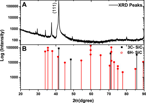
FIGURE 1. Comparison of the X-ray diffraction pattern of the as-received SiC sample. (A) with data from ICSD database (Belsky et al., 2002) No. 28389 for 3C-SiC and No. 15325 for 6H-SiC (B).
Some of the implanted polycrystalline SiC wafers were irradiated with 167 MeV Xe+26 at room temperature to fluences of 3.4 × 1014 cm−2 and 8.4 × 1014 cm−2. The irradiations were done using the IC-100 FLNR cyclotron at JINR, Dubna, Russia. The SHIs irradiation was done to in order to compare both the microstructure of the substrate in the initially implanted SiC (with Sr ions) layer and after SHIs irradiation to different fluences.
Simulation of the Sr implantations and Xe irradiation into SiC were performed using SRIM 2010 (Ziegler et al., 2010). Figure 2A shows the Sr simulated results: the Sr depth profile in SiC and displacements per atom (dpa) caused by 360 keV Sr ions implantation. Figure 2B shows the Xe simulated results: Xe depth profile in SiC, the dpa caused by 167 MeV Xe ions irradiation and the electronic energy loss of the penetrating Xe ions. In the simulation, threshold displacement energies of 20 and 35 eV for C and Si were used (Weber et al., 2004), respectively. From Figure 2A, since the minimum dpa required to amorphized the SiC is 0.3 dpa (Weber et al., 1998), Sr implantation into SiC will result in an amorphous layer of about 205 nm thickness. Moreover, the distribution character of dpa is similar to that of Sr ion concentration, but the dpa tends to aggregate the shallow surface due to collision cascade between implanted Sr ion and the substrate ones. The maximum dpa value is 2.8 dpa at the depth of 100 nm, indicating that in this area, the displacement of average atom deviates from its equilibrium position is 2.8 dpa. The SiC samples were initially implanted with 360 keV Sr ions and then irradiated with 167 MeV Xe ions. From Figure 2B, it is clear that the amorphous region in as-implanted SiC (the region from the surface of the sample to the depth of 205 nm) will be extensively exposed to large amounts of energy deposition (∼20 keV/nm) due to electronic energy loss of the penetrating Xe ions. Moreover, the nuclear energy loss from SHIs on the surface of SiC is negligible, see Figure 2B. Therefore, the large amounts of energy deposited by the Xe ions (due to electronic energy loss) in the amorphous SiC region, may cause some annealing of the radiation damage (Abdelbagi et al., 2019b).
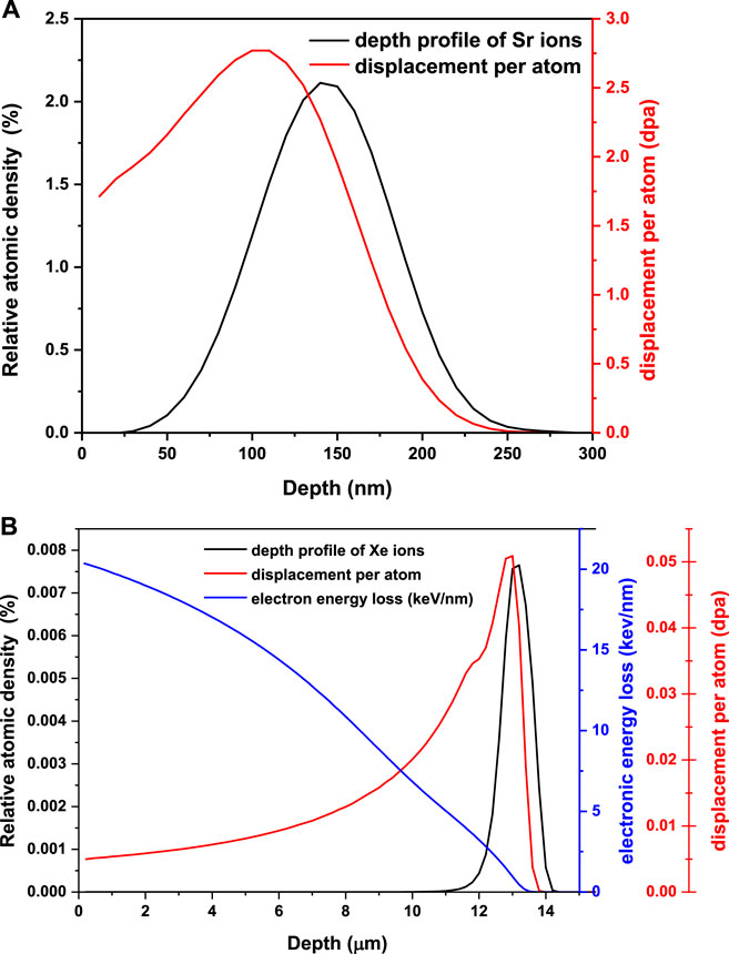
FIGURE 2. Simulated depth profiles and displacement per atom (dpa) obtained using SRIM 2010 (Ziegler et al., 2010), (A) 360 keV Sr depth profile and displacement per atom caused by implantations of Sr ions (B) depth profile of Xe of 167 MeV irradiated into SiC, the relative atomic density is shown in black, displacement per atom (dpa) in blue and electronic energy loss in red.
Both implanted and implanted then irradiated samples were annealed under vacuum using a high vacuum computer-controlled Webb 77 graphite furnace. The implanted and implanted then irradiated samples were isochronally annealed at temperatures ranging from 1,100 to 1,400°C in steps of 100°C for 5 h. Scanning electron microscopy (SEM) was used to study the topography of the SiC surfaces after implantation, SHIs irradiation and sequential annealing. The surface topographies were analyzed by a high-resolution Zeiss Ultra Plus 55 field emission scanning electron microscope (FE-SEM)and operated at 2 kV under vacuum. The FE-SEM column was evacuated to 10–5 Torr by a mechanical pump to prevent electron scattering by the residual gas molecules.
Raman spectroscopy was used to monitor the microstructural changes of SiC after that the implantation, SHIs irradiation and annealing. The Raman spectra of the SiC samples were obtained using a T64000 series II triple spectrometer system from HORIBA Scientific, Jobin Yvon Technology. An Ar+ laser (Coherent Innova® 70C series)line was used with a resolution of 2 cm−1 in the range of 200 cm−1–1800 cm−1. Moreover, the laser spot size on the samples was approximately 2 μm. The measurements were obtained in a backscattering configuration with an Olympus microscope attached to the instrument (using an LD 50 × objective). To avoid sample heating, the laser power was kept below 1.7 mW. An integrated triple spectrometer was used in the double subtractive mode to provide goodRayleighscatteredlightrejectionanddispersed the light onto a liquid nitrogen cooled Symphony CCD detector. The Raman spectra were recorded under these conditions and normalized to have the same scale. To analyse the obtained Raman spectra, the baseline of the spectral lines was corrected using a linear background correction. Some of the Raman peaks were fitted to either a Gaussian or Lorentzian function to determine the width [i.e., full width at half maximum (FWHM)] of the peak using the OriginLab software program (Edwards, 2011).
Backscattering spectrometry (RBS) was used to determine the retained ratio of implanted Sr in the as-implanted and SHIsirradiated SiC samplesbefore and after annealing. This was calculated by dividing the total counts/yield of Sr after annealing with the counts of the as-implanted sample. RBS was performed using Helium ions which were generated and accelerated to energy of 1.6 MeV using a Van de Graaff accelerator at the University of Pretoria. The backscattered He+ ions were detected using a silicon surface barrierdetector set at a 165° and charge of 8 μC was collected per measurement.
From our previous analysis of the same SiC substrate (Abdelbagi et al., 2019a), the Raman spectra of the virgin SiC sample consisted of sharp and well resolved peaks located around 794 and 964 cm−1, which are respectively attributed to the 3C-SiC transverse optical (TO) and longitudinal optical (LO) signatures (reproduced in Figure 3). The peak at 766 cm−1 represents the TO phonon mode of hexagonal polytype 6H-SiC (Lina et al., 2012). The Raman spectra is in good agreement with the XRD results (see Figure 1) which showed the presence of a small fraction of hexagonal polytypes within the 3C-SiC substrate. The two peaks at ∼1,520 cm−1 and ∼1710 cm−1 are second order TO peaks (Windl et al., 1994; Talwar, 2015), which further indicate the crystalline quality of the SiC wafers. As expected, implantation of Sr into SiC at room temperature resulted in the disappearance of the characteristic SiC Raman peaks at 766, 794 and 964 cm−1, and appearance ofbroad peaks between 700 and 1,000 cm−1. Furthermore, broad peaks around 518 cm−1 and 1,425 cm−1 were observed due to Si-Si and C-C vibrations, respectively. Thisindicates the amorphization of SiC layer after implantation with Sr ions. The amorphization of SiC after implantation with Sr ions at room temperature was extensively discussed in our previous studies (Friedland and Hlatshwayovan der Berg, 2013; Abdelbagi et al., 2019a).
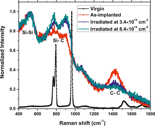
FIGURE 3. Raman spectra of the virgin SiC (virgin), implanted with 360 keV Sr ions (as-implanted), implanted with Sr then irradiated with 167 MeV Xe ions to fluences of 3.4 × 1014 cm−2and of 8.4 × 1014 cm−2.
Irradiation of the implanted SiC with Xe (167 MeV) ions at room temperature to fluences of 3.4 × 10¹⁴ and 8.4 × 1014 cm−2 caused the partial reappearance of the broad Si-C characteristic Raman peaks at around 775 and 900 cm−1with the C-C (around 1,425 cm−1) and Si-Si (around 525 cm−1) peaks still present (see Figure 3). The appearance of the SiC characteristic peaks albeit broad indicates some limited recrystallization of the initially amorphous SiClayer.Similar recrystallization of SiC pre-damaged by different implanted ions after SHIs irradiation has been reported previously (Debelle et al., 2012; Hlatshwayo et al., 2015; Hlatshwayo et al., 2016; Abdelbagi et al., 2019b; Abdelbagi et al., 2022). In our previous studies, transmission electron microscopy (TEM) and Raman spectroscopy were used to study the structural changes of the as-implanted SiC after SHIs irradiation (Hlatshwayo et al., 2015; Hlatshwayo et al., 2016; Abdelbagi et al., 2019b; Abdelbagi et al., 2022). We found that, the recrystallization of the initially amorphous SiC was due to SHIs irradiation causing the formation of randomly oriented crystallites embedded withinthe amorphous SiC. The similarities of the reported Raman results in the previous works (Hlatshwayo et al., 2015; Hlatshwayo et al., 2016; Abdelbagi et al., 2019b; Abdelbagi et al., 2022) with our current Raman results (in Figure 3) suggest that the irradiated amorphous SiC layer is composed of randomly oriented crystallites embedded in amorphous SiC.
Figure 4 shows the SEM images of the virgin, as-implanted and irradiated samples. The SEM image of the virgin sample showed some polishing marks on the surface (Figure 4A,A’), which partially disappeared after implantation with 360 keV Sr at room temperature, see Figure 4B,B’. In a previous study, implantation with 360 keV Ag (at room temperature) into the virgin SiC caused the total disappearance of the polishing marks (Abdelbagi et al., 2022). The disappearance of polishing marks inas-implanted SiC surface is due to swelling of the SiC after to amorphization (Snead et al., 1998). Moreover, if one assumes the swelling of SiC at 3 dpa is regarded as a saturated swelling (Katoh et al., 2002), it is quite clear that implantation of 360 keV Ag ions (with maximum dpa >3 (Abdelbagi et al., 2022)) will result in more swelling as compared to the swelling in the SiCimplanted with 360 keV Sr ions (with maximum dpa <2.5—see Figure 2A). Therefore, implantation of Ag at room temperature into the virgin SiC caused disappearance of more polishing marks as compared the SiC samples implanted with Sr at room temperature. Due to the disappearance of the polishing marks caused by the swelling of SiC after to amorphization (Snead et al., 1998), the SEM analysis also confirmed the amorphization of SiC afterimplantation as revealed by SRIM and Raman analysis in Figures 2, 3, respectively. Moreover, due to surface swelling, the SiC surface becomes smooth after implantation at room temperature, and thus, the surface roughness of the implanted samples will not affect the Raman scattering. Therefore, the broadening in the FWHM of the characteristic SiC peaks after implantation (see Figure 3) is due to radiation damage and surface roughness played no role in this change.
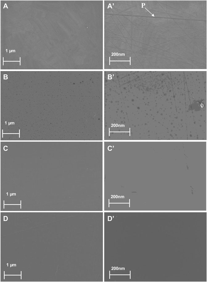
FIGURE 4. SEM micrographs of the CVD-SiC surface. Low magnification images of (A) the as-received, (B) as-implanted with Sr, (C) implanted with Sr then irradiated with Xe ions to a fluence of 3.4 × 1014 cm−2 and (D) implanted with Sr then irradiated with Xe ions to a fluence of 8.4 × 1014 cm−2 (A’), (B’), (C’) and (D’) are the corresponding high magnification SEM images.
Since the Raman spectra ofthe irradiated samples (in Figure 3) showed partial recrystallization of the room temperature as-implanted SiC, one would expect to see some crystallinity in SEM images of the SHIsirradiated SiC surface (Figure 4C,C’ and Figure 4D,D’). The inability to see changes in the irradiated samples compared to as-implanted sample implies that the random crystallites in the SHIs irradiated samples are below the SEM detection limit.
Raman spectra of as-implanted and SHIs irradiatedsamples after annealing at 1,100°C are shown in Figure 5. Annealing the SHIs irradiated and as-implanted samples at 1,100°C resulted in the reappearance of SiC characteristic peaks. As extensively discussed in (Abdelbagi et al., 2019a), theas-implanted samples were fully recrystallized, while the SHIs irradiated samples were poorly recrystallized (see Figure 5A). The difference in the recrystallization in these samples is due to the amount of impurities (i.e., concentration of implanted Sr atoms) within the substrate after annealing at 1,100°C see Figure 6.
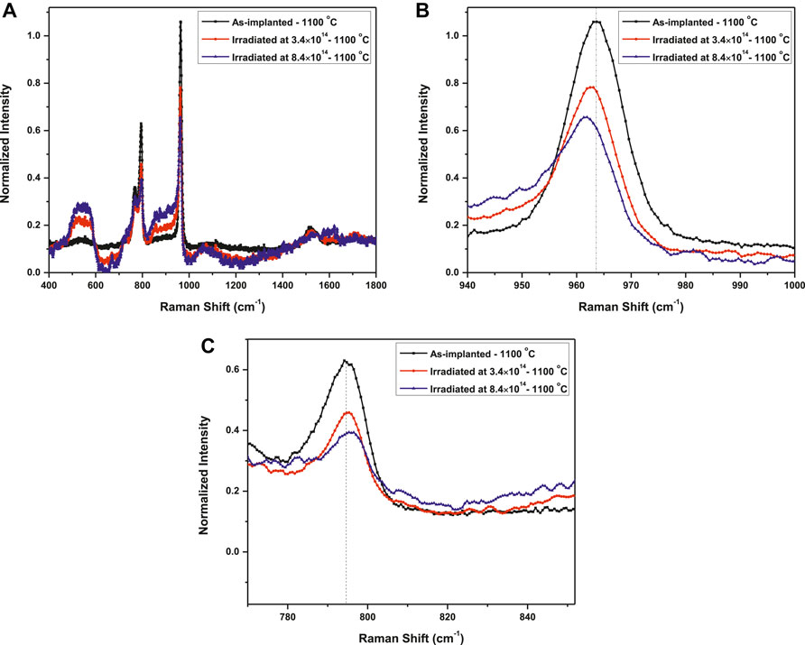
FIGURE 5. Raman spectra of (A) SiC implanted with Sr at room temperature then annealedat 1,100°C (As-implanted-1100°C), implanted and then irradiated with 167 MeV Xe ions to fluences of 3.4 × 1014 cm−2 and 8.4 × 1014 cm−2and finally annealed at 1,100°C. (B) and (C) the Raman spectra only show the LO and TO mode, respectively, with a dashed line representing LO and TO peak positions of the as-implanted samples annealed at 1,100°C.
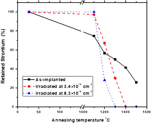
FIGURE 6. The retained ratio of strontium in SHIs irradiated and as-implanted samples before and after sequential annealing up to 1,500°C.
Figure 6 shows the retained ratio (obtained from RBS spectra (not shown)) of implanted Sr atoms in SHIs irradiated and as-implanted samples after sequentially annealing from 1,100°C to 1,500°C. The retained ratio of Sr in SiC was calculated from the total counts/yield of Sr after annealing, divided by the RBS counts of the as-implanted sample. Annealing the as-implanted with Sr samples at 1,100°C resulted in poor Sr retention of about 75%. The SHIs irradiated samples retained more than 97% of implanted Sr (i.e., from the initial Sr concentration) after annealing at 1,100°C. The difference in the retained ratio of Sr in the as-implanted and SHIs irradiated samples annealed at 1,100°C is due to the fact that SHIs irradiation was enhanced the migration of Sr atoms in SiC. This was extensively discussed in our previous study (Abdelbagi et al., 2019a). In general, impurities usually retard the recrystallization process and inhibit crystal growth (Burton et al., 1951; Hirth and Pound, 1960). The impurity in this case is Sr. Therefore, the irradiated samples showed poor recrystallization due to the high amount of Srretained in SiC (more than 97%) after annealing at 1,100°C. While the as-implanted samples annealed at 1,100°C showed good recrystallization due to the small amount of Sr retained in SiC (about 75%)—see Figure 6. However, in our previous study (Abdelbagi et al., 2022), the SiC samples with high retained ratio of Ag showed good recrystallization (somehow) as compared to the sample with low retained ratio of Ag. This suggest that Ag assists the recrystallization of SiC, while Sr inhibits the recrystallization of SiC.
After annealing at 1,100°C, the observed TO and LO peaks positions for as-implanted samples were in the same positions as those of the virgin SiC (see Figures 3, 5). However, the LO phonon mode at 964 cm−1 shifted down to 962 cm−1 and 961 cm−1 for the samples irradiated to fluences of 3.4 × 1014 cm−2 and 8.4 × 1014 cm−2 respectively—see Figure 5B. Furthermore, the TO mode at 794 cm−1upshifted to 795 cm−1 and 796 cm−1 for the samples irradiated to fluences of 3.4 × 1014 cm−2 and 8.4 × 1014 cm−2 respectively—see Figure 5C. Wieligor et al. (2005) found that with a decrease in the SiC crystallite size, the LO phonon mode shifts to lower wavenumber, while the TO phonon shifts to higher wavenumber. Therefore, for the SHIs irradiated samples annealed at 1,100°C, the shift in the LO Raman peaks towards lower wavenumbers (as well as shift of the TO mode to higher wavenumber) could be due to the presence of small crystallites which formed within the amorphous region of SiC. A larger shift toward lower wavenumbers for LO peak (accompanied by larger shift toward higher wavenumbers for TO peak) was observed in the sample irradiated to a higher fluence (8.4 × 1014 cm−2), indicating even smaller crystallites as shown in Figures 5B,C.
Wieligor et al. (2005) found that with decreasing crystal size, the intensity of the SiC Raman peaks (TO and LO modes) decreased. Moreover, Liu et al. (2010) were more specific and found that as 3C–SiC nanocrystal average size increases, only the LO phonon intensity increases in the Raman spectra (i.e., LO mode property of SiC is strongly crystal size dependent). From Figure 5, the SiC LO mode of the as-implanted sample at about 964 cm−1 had a significantly higher intensity compared to that of the SHIs irradiated samples. This suggests that the as-implanted sample has on average larger crystalscompared to the SHIsirradiated samples after annealing both samples at 1,100°C.
The variations in Raman peakpositions and intensities were accompanied by an increase in the full width at half maximum (FWHM) of the SiC Raman prominent peak (i.e., LO mode) from 9.4 cm−1 (virgin) to 11.6 cm−1 for the as-implanted samples, 11.8 cm−1 and 19.6 cm−1 for irradiated samples to fluences of 3.4 × 1014 cm−2 and 8.4 × 1014 cm−2 respectively (see Figure 7). Figure 7 shows the FWHM, intensity and peak position of LO mode in the virgin SiC, as-implanted and SHIs irradiated samples after sequentially annealing from 1,100°C to 1,400°C.Feng et al. (Feng and Zang, 2016) found that the structural defects in SiC reduced the phonon lifetime, and hence caused a broadening of phonon Raman bands. Thus, the increase in the FWHM indicates the existence of some kind of disordering. Furthermore, Wieligor et al. (2005) and Qiang et al. (2013).suggested that thebroadening in the FWHM of the SiC characteristic peaks is due to the decrease in crystal size in SiC.The FWHM of the as-implanted sample was narrower compared to the SHIsirradiated samples—see Figure 7. This confirms that annealing the as-implantedsamples at 1,100°C resulted in larger crystallites compared to SHIsirradiated samples annealed in the same conditions.
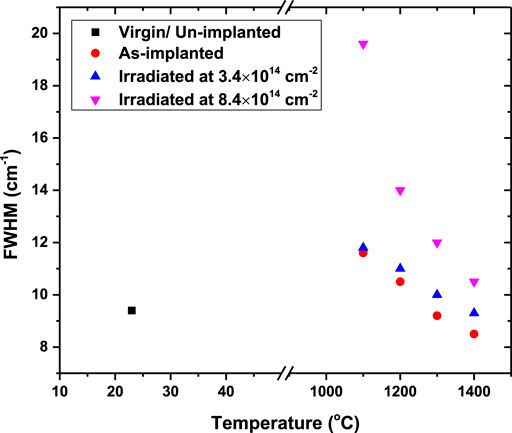
FIGURE 7. The FWHM of the LO mode of the as-implanted and SHIs-irradiated samples as function of temperature.
The crystallization observed by Raman spectroscopy in Figure 5 (for the samples annealed at 1,100°C) was also evident in the SEM images shown in Figure 8. After implantation the surfaces were featureless (excluding some of the polishing marks), as is typical of bombardment induced amorphous SiC layers (Malherbe, 2013) as shown in Figure 4B. However, annealing of the as-implanted samples at 1,100°C resulted in appearance of crystals which shows evidence of recrystallization—see Figure 8A,A’. Some pores can also be seen on the surface of this sample. There are some changes on the surface of the irradiated sample at low fluence (i.e.,3.4 × 1014 cm−2) after annealing at 1,100°C while there are no major changes on the surface of the sample irradiated at higher fluence (i.e., 8.4 × 1014 cm−2) after annealing at the same temperature (see Figure 4C’D’ and Figure 8B’C’). The featureless surface of the samples irradiated at higher fluence (i.e., 8.4 × 1014 cm−2) after annealing at 1,100°C indicates that there aresmaller crystallites on the surface compared to samples irradiated to lower fluence. Thiscorrelates with the Raman results in Figure 5, where the LO peak of the sample irradiated to a fluence of 8.4 × 1014 cm−2 had a larger shift toward lower wavenumbers, lower LO peak intensity and larger FWHM(see Figure 7) which indicatesthe presence of smaller crystallites.
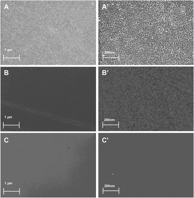
FIGURE 8. SEM micrographs of samples annealed at 1,100°C. Low magnification images are shown of (A) as-implanted, (B) SHIs irradiated sample to a fluence of 3.4 × 1014 cm−2 and (C) 8.4 × 1014 cm−2. The corresponding high magnification images are shown in (A’), (B’), and (C’).
Thesevariations in the average crystallite size between the SHIsirradiated and as-implanted samples can be explained by the nucleation rate per unit amorphous area (Kurtenbach et al., 1998). The high rate of nucleation will produce many tiny crystals that would make the size of the individual crystals smaller compared to the samples with low nucleation rate which produce larger size of crystals (Kurtenbach et al., 1998; Abdelbagi et al., 2022). As discussed above (in Figure 3), the formation of randomly orientated nanocrystals in an amorphous matrix after SHIs irradiation (i.e., high nucleation rate per unit amorphous area) was extensively investigated using transmission electron microscopy (TEM) as presented in our previous work (Hlatshwayo et al., 2015; Hlatshwayo et al., 2016; Abdelbagi et al., 2022). From Figures 3, 4, the as-implanted samples were amorphous before annealing (i.e., with low nucleation rate). Therefore, the crystal size would be larger in the as-implanted samples as compared to the SHIsirradiated samples which were composed of crystallites that were randomly orientated in an amorphous matrix before annealing (Hlatshwayo et al., 2015; Hlatshwayo et al., 2016; Abdelbagi et al., 2022). Hereafter, the differences in the average crystal sizes between the SHIsirradiated and as-implanted samplesisbecause the initial surfaces/layers were in different states before annealing (as mentioned above in Figure 3), i.e., the as-implanted samples were amorphous while the SHIsirradiated samples were partially recrystallized.
The nano-crystallites in the SHIs irradiated samples annealed at 1,100°C (which were not visible in SEM images—see Figure 8B,B’ and Figure 8C,C’ are more clearly visible after annealing these samples at 1,200°C as can be seen in Figure 9B,C,B’C’. Also, more pores appeared on the surfaces of the irradiated samples annealed at 1,200°C. A comparison of the results in Figure 8B,C,B’C’ and Figure 9B,C,B’C’ shows that the increase in temperature which increases the mobility of atoms led to the increase in average crystal size, in line with crystal growth theory (Burton et al., 1951; Hirth and Pound, 1960). Furthermore, it has been observed that the changes in the surface of SiC after annealing are not due to surface oxidation or contamination but are due to surface diffusion and grain growth. Rutherford backscattering spectroscopy (RBS) was used to confirm that there was not oxidation or contamination in the SiC surface during vacuum annealing. In the RBS spectra (not included here), no other elements (other than Si, C and Sr) were observed for the annealed samples, indicating that there was no contamination on the SiC surface and that the annealing was carried out in a suitable vacuum.
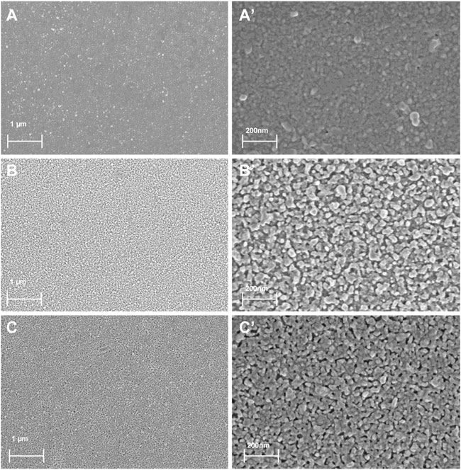
FIGURE 9. SEM micrographs of samples annealed at 1,200°C. Low magnification images are shown of (A) as-implanted, (B) irradiated with Xe to a fluence of 3.4 × 1014 cm−2 and (C) irradiated with Xe to a fluence of 8.4 × 1014 cm−2. The corresponding high magnification images are shown in (A’), (B’), and (C’).
The average crystal size of the as-implanted and SHIs irradiated samples annealed at 1,200°C were determined from the SEM images in Figure 9 using ImageJ program (Ferreira and Rasband, 2011). The crystal size was measured with respect to the scale of the SEM image (i.e., 200 nm). Five straight lines were drawn randomly across the SEM images (to ensure that the crystals were selected randomly) and the sizes of individual crystals along these lines were determined and averaged. Since the surface of as-implanted and SHIs irradiated samples contain pores (see Figure 9), the average pore size was also determined with respect to the scale of the SEM image (i.e., 200 nm). The average crystal and pore size for the samples annealed at 1,200°C are listed in Table 1. From Table 1, the nano-crystallites on the SHIs irradiated samples annealed at 1,100°C (which were not visible in SEM images) were clearly appeared after annealing at 1,200°C (see Figure 9B,C,B’C’) and have average crystal size of about 67 and 56 nm for irradiated samples to fluences of 3.4 × 1014 cm−2 and 8.4 × 1014 cm−2, respectively see Figure 9 and Table 1. However, the as-implanted samples still have larger average crystal size (i.e., 89 nm) as compared to the crystals in the SHIs irradiated samples, all annealed at 1,200°C. This can be proven by Raman spectra of the as-implanted and SHIs irradiated samples annealed at 1,200°C, as shown in Figure 10 below.
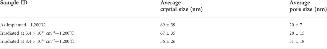
TABLE 1. Average crystal and pores sizes determined from SEM images for as-implanted and SHIs irradiated SiC sample annealed at 1,200°C.
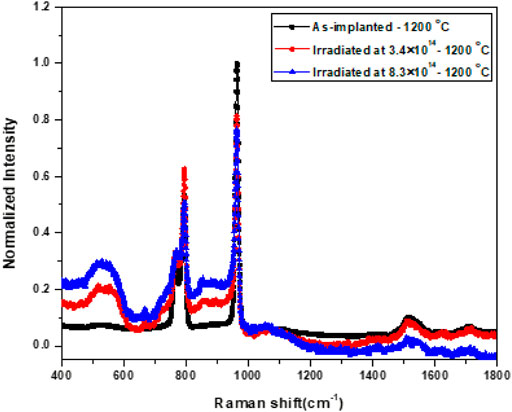
FIGURE 10. Raman spectra of SiC implanted with Sr at room temperature then annealed at 1,200°C (As-implanted—1,200°C), implanted and then irradiated with Xe ions to fluences of 3.4 × 1014 cm−2 and 8.4 × 1014 cm−2 and finally annealed at 1,200°C.
After annealing the as-implanted and SHIs irradiated samples at 1,200°C, the Raman spectra showed increased narrowing of the TO and LO modes of SiC indicating more recovery (i.e., recrystallization) of the SiC structure (Feng and Zang, 2016), due to annealing at 1,200°C as seen in Figure 10. At 1,200°C, as-implanted samples had higher LO mode intensity (see Figure 10) and a larger average crystals size (see Table 1) compared to the irradiated samples annealed in the same conditions. Furthermore, the samples irradiated to a fluence of 3.4 × 1014 cm−2 had a large average crystals size (67 nm) and high LO mode intensity (see Figure 10) compared to the samples irradiated to a fluence of 8.4 × 1014 cm−2. Thus, as the average crystal size increases, the LO mode intensity increases in the Raman spectra.
The average crystal size of as-implanted and SHIs irradiated samples annealed at 1,300°C and 1,400°C were determined from the SEM images in Figures 11, 12, respectively. The average crystal and pore size for the as-implanted and SHIs irradiated samples after sequentially annealing up to 1,300°C and 1,400°C are listed in Table 2, which show that the SiC crystallites increased in size with the increase in annealing temperature, in line with crystal growth theory (Burton et al., 1951; Hirth and Pound, 1960). From Table 2, the SHIs irradiated samples annealed at 1,300°C showed larger average crystal size compared to the as-implanted samples annealed under same conditions. This is rather surprising, as the as-implanted samples had already larger average crystal size after annealing up to 1,200°C compared to the SHIs irradiated samples. At 1,300°C, 0% and 30% of implanted Sr was retained in the 8.4 × 1014 cm−2 and 3.4 × 1014 cm−2 irradiated samples respectively (see Figure 6). While the as-implanted samples have retained more than 50% of Sr atoms after annealing at 1,300°C. As mentioned above, the presence of impurities inhibits crystal growth (Burton et al., 1951; Hirth and Pound, 1960). Therefore, due to the low amount of the retained Sr atoms in the irradiated samples after annealing at 1,300°C, the SHIs irradiated samples showed larger average crystal size compared to the as-implanted samples.
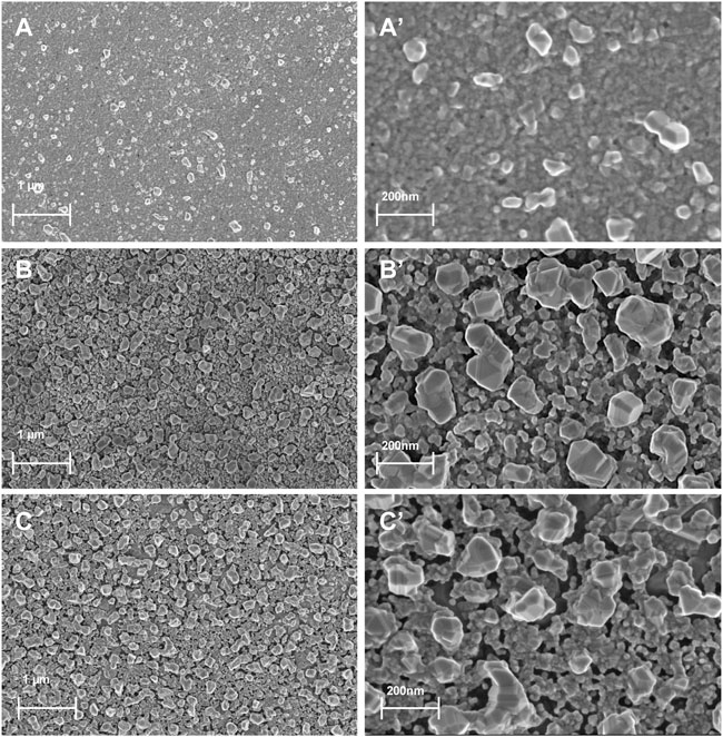
FIGURE 11. SEM micrographs of samples annealed at 1,300°C. Low magnification images are shown of (A) as-implanted, (B) irradiated with Xe to a fluence of 3.4 × 1014 cm−2 and (C) irradiated with Xe to a fluence of 8.4 × 1014 cm−2. The corresponding high magnification images are shown in (A’), (B’), and (C’).

FIGURE 12. SEM micrographs of samples annealed at 1,400°C. Low magnification images are shown of (A) as-implanted, (B) irradiated with Xe to a fluence of 3.4 × 1014 cm−2 and (C) irradiated with Xe to a fluence of 8.4 × 1014 cm−2. The corresponding high magnification images are shown in (A’), (B’), and (C’).
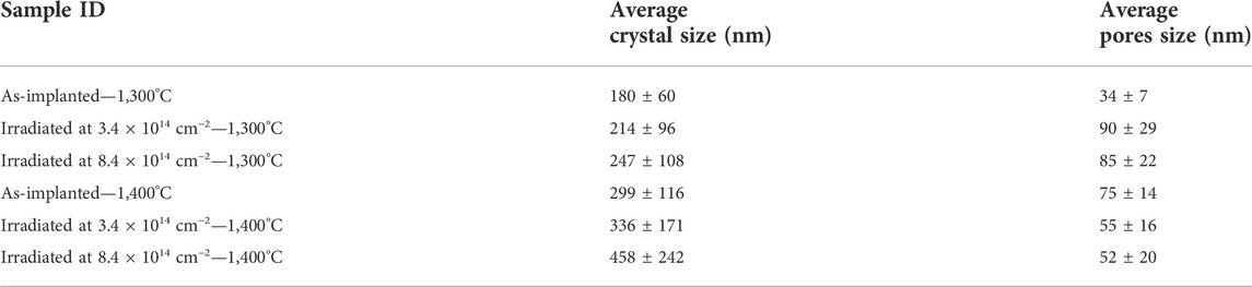
TABLE 2. Average crystal and pores sizes determined from SEM images for as-implanted and SHIs irradiated SiC annealed at 1,300 and 1,400°C.
The Raman spectra of the as-implanted and SHIs irradiated samples after sequentially annealing up to 1,300°C are shown in Figure 13. As the average crystal size (see Figure 11 and Table 2) for the SHIs irradiated samples annealed at 1,300°C are larger than the as-implanted samples annealed under the same conditions, one would expect to see higher LO modes intensities for the SHI irradiated samples compared to as-implanted samples. Newby et al. (2011) studied the differences between the Raman spectra of the bulk SiC and those of porous SiC. They found that the intensity of LO mode decreased and shifted to higher wavenumbers in the Raman spectrum of the porous SiC compared to Raman spectrum of the bulk SiC. The results presented by Newby et al. (2011) are in agreement with our observations, where the LO mode of the Raman spectrum of the SHI irradiated SiC samples (with large pore sizes-see Table 2 and Figure 11) showed lower intensity and shifted to high wavenumbers (see Figure 13B). Therefore, the reduction of LO mode intensities in the SHI irradiated samples could be due to the large size and number of pores in the irradiated SiC which decreases the area of interaction between Raman laser beam and the surface of the sample (see Table 2 and Figure 11). Thus, the presence of pores can play a role in the decrease of the LO mode intensity even if the average crystal size is large.
FIGURE 13. Raman spectra of (A) as-implantedand SHIs irradiated. SiC sequentially annealed up to 1,300°C. (B) the Raman spectra only show the LO mode.
After annealing at 1,400°C, the crystal growth led to coalescing of crystals as shown in Figure 12B,B’C,C’. From Table 2, the average crystallite size increased with fewer and smaller pores compared to the samples annealed at lower temperatures. In contrast, these pores were larger and clearly visible in the as-implanted samples annealed at 1,100°C (Figure 8A,A’) and in the SHIs irradiated samples annealed at 1,300°C (Figure 11B,B’C,C’). The same explanation of crystal growth used above is also applicable here. From Table 2, the SHIs irradiated samples annealed at 1,400°C still show larger average crystal size compared to the as-implanted samples annealed under same conditions. No implanted Sr was retained in the 3.4 × 1014 cm−2 and 8.4 × 1014 cm−2 irradiated samples (see Figure 6) after annealing at 1,400°C, whereas 25% of Sr was still retained in the as-implanted samples annealed at the same conditions. As mentioned above, since the impurities can inhibit the crystal growth, the irradiated samples showed larger average crystal size compared to the as-implanted samples due to the low amount of the retained Sr atoms in the irradiated samples-all annealed at 1,400°C.
Raman spectra of the as-implanted and SHIs irradiated samples after sequentially annealing up to 1,400°C are shown in Figure 14. As the average crystal size values (see Figure 12 and Table 2) for the irradiated samples annealed at 1,400°C are larger than those of the as-implanted samples annealed under the same conditions, higher LO modes intensities for the irradiated samples compared to the as-implanted samples would be expected. However, the intensities of the LO mode of irradiated SiC samples are slightly lower than the intensity of LO mode of the as-implanted samples. Zhou et al. (2015) studied the effect of defects in 3C-SiC on the intensity of the LO mode. They found that the presence of defects in 3C–SiC thin films decreased the LO mode intensity. Some of the defects that were introduced into SHIs irradiated SiC are still present even after annealing the samples at 1,400°C (Si-Si peak at around 525 cm−1, see Figure 14). The samples irradiated to a high fluence (i.e., 8.4 × 1014 cm−2) show higher Si-Si peak intensity (which indicates the presence of more defects in SiC (Rodriguez et al., 1996) and lowest LO mode intensity. Therefore, several factors can play a role in the decrease of the LO mode intensity (even if the average crystal size is large) such as pores and defects.
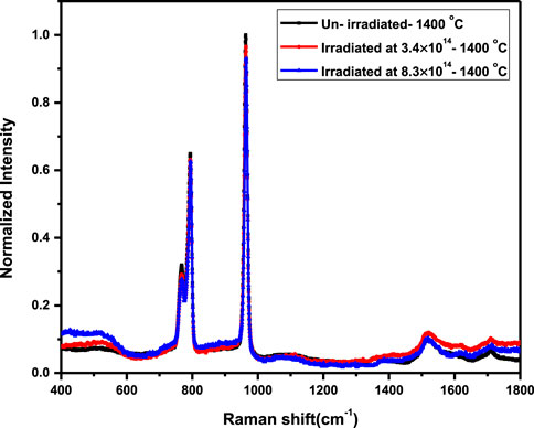
FIGURE 14. Raman spectra of as-implanted and SHIs irradiated SiC sequentially annealed up to 1,400°C.
The effects of SHIs irradiation and annealing on the recrystallization of SiC pre-implanted with Sr ions was investigated. Polycrystalline SiC was implanted with 360 keV Sr ions to a fluence of 2 × 1016 cm−2 at room temperature. Some of as-implanted samples were irradiated with Xe ions of 167 MeV to a fluence of 3.4 × 1014 cm−2 and 8.4 × 1014 cm−2 at room temperature. The as-implanted and implanted the SHIs irradiated samples were vacuum annealed from 1,100 to 1,400°C in steps of 100°C for 5 h. The average crystallite size of implanted and irradiated SiC after annealing was studied using Raman spectroscopy and scanning electron microscopy. Implantation of 360 keV Sr (up to a fluence of 2 × 1016 cm−2) ions in polycrystalline SiC at room temperature caused amorphization of SiC, while SHIs irradiation of the as-implanted SiC resulted in limited recrystallization of the initially amorphized SiC. Annealing the as-implanted samples at 1,100°C caused full recrystallization of SiC resulting in the appearance of the SiC characteristic Raman peaks. However, annealing the SHIs irradiated SiC samples at 1,100°C showed poor recrystallization with a broad Si-Si peak and C-C peak. The differences in the recrystallization between the as-implanted and SHIs irradiated samples annealed at 1,100°C was due to the amount of impurities (i.e., concentration of implanted Sr atoms) retained within the SiC substrate. At 1,100°C, the samples with low Sr retained ratio (as-implanted samples) showed full recrystallization, while the samples with high Sr retained ratio (SHIs irradiated samples) showed poor recrystallization. This suggests that the presence of Sr within the implanted region inhibited the recrystallization of SiC.
For the annealing temperatures ≤1,200°C, the SHIs irradiated samples had smaller crystals and more crystals defects (i.e., larger FWHM in the Raman modes) as compared to the as-implanted samples annealed at the same conditions. However, for the annealing temperature ≥1,300°C, the SHIs irradiated samples had larger crystals as compared the as-implanted samples annealed at the same conditions. The SHIs irradiated samples growth faster than the as-implanted samples (after annealing at temperature ≥1,300°C), due to the absence of impurities (i.e., Sr atoms) from the SHIs irradiated samples.
Raman spectroscopy and SEM results showed that the as-implanted sample (annealed sequentially at 1,100°C and 1,200°C) had on average larger crystals and higher LO mode intensities compared to the SHIs irradiated samples annealed in the same conditions. This suggests that the intensity of the longitudinal optical (LO) phonon in Raman spectra increases with increasing the average crystal sizes of SiC. However, at 1,300 and 1,400°C, SEM and Raman showed that the SHIs irradiated samples had showed larger crystals and lower LO mode intensity compared with the as-implanted sample annealed in the same conditions. The reduction of LO mode intensities for the SHIs irradiated samples annealed at 1,300 and 1,400°C is due to the large number of pores and defects in the irradiated SiC, respectively. Therefore, the intensity of the LO mode of SiC can decrease (even if the average crystal size is large) due to the presence of pores and defects in the 3C-SiC.
The original contributions presented in the study are included in the article/supplementary material, further inquiries can be directed to the corresponding author.
HA: Conceptualization, Methodology, Software, Investigation, Writing—original draft. VS: Investigation, Writing—review and editing. EN: Writing—review and editing. MM: Writing—review and editing. TH: Writing—review and editing. JM: Resources, Writing—review and editing, Supervision. TJ: Writing-review and editing.
Financial support by the National Research Foundation of South Africa (grant numbers 120808) is gratefully acknowledged.
Author MM was employed by the company Mintek.
The remaining authors declare that the research was conducted in the absence of any commercial or financial relationships that could be construed as a potential conflict of interest.
All claims expressed in this article are solely those of the authors and do not necessarily represent those of their affiliated organizations, or those of the publisher, the editors and the reviewers. Any product that may be evaluated in this article, or claim that may be made by its manufacturer, is not guaranteed or endorsed by the publisher.
Abdelbagi, H. A. A., Skuratov, V. A., Adeojo, S. A., Mohlala, T. M., Hlatshwayo, T. T., and Malherbe, J. B. (2022). Effect of SHI irradiation and high temperature annealing on the microstructure of SiC implanted with Ag. Nucl. Instrum. Methods Phys. Res. Sect. B Beam Interact. Mater. Atoms 511, 18–29. doi:10.1016/j.nimb.2021.11.016
Abdelbagi, H. A. A., Skuratov, V. A., Motloung, S. V., Njoroge, E. G., Mlambo, M., Hlatshwayo, T. T., et al. (2019). Effect of swift heavy ions irradiation on the migration behavior of strontium implanted into polycrystalline SiC. Nucl. Instrum. Methods Phys. Res. Sect. B Beam Interact. Mater. Atoms 451, 113–121. doi:10.1016/j.nimb.2019.05.039
Abdelbagi, H. A. A., Skuratov, V. A., Motloung, S. V., Njoroge, E. G., Mlambo, M., Malherbe, J. B., et al. (2019). Effect of swift heavy ions irradiation in the migration of silver implanted into polycrystalline SiC. Nucl. Instrum. Methods Phys. Res. Sect. B Beam Interact. Mater. Atoms 461, 201–209. doi:10.1016/j.nimb.2019.10.002
Belsky, A., Hellenbrandt, M., Karen, V. L., and Luksch, P. (2002). New developments in the inorganic crystal structure database (ICSD): Accessibility in support of materials research and design. Acta Crystallogr. B 58, 364–369. doi:10.1107/s0108768102006948
Burton, W. K., Cabrera, N., and Frank, F. C. (1951). The growth of crystals and the equilibrium structure of their surfaces. Phil. Trans. Roy. Soc. A 243, 299–358.
Debelle, A., Backman, M., Thome, L., Weber, W. J., Toulemonde, M., Mylonas, S., et al. (2012). Combined experimental and computational study of the recrystallization process induced by electronic interactions of swift heavy ions with silicon carbide crystals. Phys. Rev. B 86, 100102. doi:10.1103/physrevb.86.100102
Debelle, A., Thom´e, L., Dompoint, D., Boulle, A., Garrido, F., Jagielski, J., et al. (2010). Characterization and modelling of the ion-irradiation induced disorder in 6H-SiC and 3C-SiC single crystals. J. Phys. D. Appl. Phys. 43, 455408. doi:10.1088/0022-3727/43/45/455408
Dwaraknath, S., and Was, G. S. (2014). Development of a multi-layer diffusion couple to study fission product transport in β-SiC. J. Nucl. Mater. 444, 170–174. doi:10.1016/j.jnucmat.2013.09.040
Dwaraknath, S., and Was, G. S. (2016). The diffusion of Cesium, Strontium, and Europium in silicon carbide. J. Nucl. Mater. 476, 155–167. doi:10.1016/j.jnucmat.2016.04.034
Feng, X., and Zang, Y. (2016). Raman scattering properties of structural defects in SiC. Proce. 3rd Inter. Conf. Mech. Inf. Tech.
Friedland, E., and Hlatshwayovan der Berg, T. T. andN. G. (2013). Influence of radiation damage on diffusion of fission products in silicon carbide. Phys. Status Solidi C 10, 208–215. doi:10.1002/pssc.201200457
Friedland, E., Malherbe, J. B., van der Berg, N. G., Hlatshwayo, T., Botha, A. J., Wendler, E., et al. (2009). Study of silver diffusion in silicon carbide. J. Nucl. Mater. 389, 326–331. doi:10.1016/j.jnucmat.2009.02.022
Friedland, E., van der Berg, N. G., Malherbe, J. B., Wendler, E., and Wesch, W. (2012). Influence of radiation damage on strontium and iodine diffusion in silicon carbide. J. Nucl. Mater. 425, 205–210. doi:10.1016/j.jnucmat.2011.10.032
Goldberg, Yu., Levinshtein, M., and Rumyantsev, S. (2001). “Silicon carbide (SiC),” in Properties of advance semiconductor materials. Editors M. Levinshtein, S. Rumyantsev, and Shur (Wiley).
Gurban, S., Kotis, L., Pongracz, A., Sulyok, A., Toth, A. L., Vazsonyi, E., et al. (2015). The chemical resistance of nano-sized SiC rich composite coating. Surf. Coat. Technol. 261, 195–200. doi:10.1016/j.surfcoat.2014.11.032
Hirth, J. P., and Pound, G. M. (1960). Coefficients of evaporation and condensation. J. Phys. Chem. 64, 619–626. doi:10.1021/j100834a024
Hlatshwayo, T. T., Mtshonisi, N., Njoroge, E. G., Mlambo, M., Msimanga, M., Skuratov, V. A., et al. (2020). Effects of Ag and Sr dual ions implanted into SiC. Nucl. Instrum. Methods Phys. Res. Sect. B Beam Interact. Mater. Atoms 472, 7–13. doi:10.1016/j.nimb.2020.03.035
Hlatshwayo, T. T., O'Connell, J. H., Skuratov, V. A., Wendler, E., Njoroge, E. G., Mlambo, M., et al. (2016). Comparative study of the effect of swift heavy ion irradiation at 500 oC and annealing at 500 oC on implanted silicon carbide. RSC Adv. 6, 68593–68598. doi:10.1039/c6ra13592g
Hlatshwayo, T. T., O’Connell, J. H., Skuratov, V. A., Msimanga, M., Kuhudzai, R. J., Njoroge, E. G., et al. (2015). Effect of Xe ion (167 MeV) irradiation on polycrystalline SiC implanted with Kr and Xe at room temperature. J. Phys. D. Appl. Phys. 48, 465306. doi:10.1088/0022-3727/48/46/465306
Katoh, Y., Kishimoto, H., and Kohyama, A. (2002). Low temperature swelling in Beta-SiC associated with point defect accumulation. Mat. Trans. 43, 612–616. doi:10.2320/matertrans.43.612
Kurtenbach, D., Martin, H., Roewer, E. M G., and Hoell, A. (1998). Crystallization of polymer derived silicon carbide materials. J. Eur. Ceram. Soc. 18, 1885–1891. doi:10.1016/s0955-2219(98)00136-8
Lina, S., Chena, Z., Lib, L., and Yang, C. (2012). Effect of impurities on the Raman scattering of 6H-SiC crystals. Mat. Res. 15, 833–836. doi:10.1590/s1516-14392012005000108
Liu, L. Z., Wang, J., Wu, X. L., Li, T. H., and Chu, P. K. (2010). Longitudinal optical phonon–plasmon coupling in luminescent 3C–SiC nanocrystal films Opt. Lett. 35, 4024–4026. doi:10.1364/ol.35.004024
Malherbe, J. B., Friedland, E., and van der Berg, N. G. (2008). Ion beam analysis of materials in the PBMR reactor. Nucl. Instrum. Methods Phys. Res. Sect. B Beam Interact. Mater. Atoms 266, 1373–1377. doi:10.1016/j.nimb.2007.10.046
Malherbe, J. B. (2013). Topical Review: Diffusion of fission products and radiation damage in SiC. J. Phys. D. Appl. Phys. 46 (27), 473001. doi:10.1088/0022-3727/46/47/473001
Newby, P., Bluet, J., Aimez, V., Fréchette, L. G., and Lysenko, V. (2011). Structural properties of porous 6H silicon carbide. Phys. Status Solidi C 8, 1950–1953. doi:10.1002/pssc.201000222
Edwards, P. M. (2011). Origin 7.0: Scientific graphing and data analysis software. J. Chem. Inf. Comput. Sci. 42 (2002), 1270–1271. (Accessed March 09, 2018).
Petti, D. A., Demkowicz, P. A., Maki, J. T., and Hobbins, R. R. (2012). TRISO-Coated particle fuel performance. Compr. Nucl. Mat. 3, 151–213.
Qiang, X., Li, H., Zhang, Y., Tian, S., and Wei, J. (2013). Synthesis and Raman scattering of SiC nanowires decorated with SiC polycrystalline nanoparticles. Mater. Lett. 107, 315–317. doi:10.1016/j.matlet.2013.06.055
Rodriguez, A. P., Pacaud, Y., Barrio, L. C., Serre, C., Skorupa, W., and Morante, J. R. (1996). Analysis of ion beam induced damage and amorphization of 6H-SiC by Raman scattering. J. Electron. Mat. 25, 541–547. doi:10.1007/bf02666633
Snead, L. L., Zinkle, S. J., Hay, J. C., and Osborne, M. C. (1998). Amorphization of SiC under ion and neutron irradiation. Nucl. Instrum. Methods Phys. Res. Sect. B Beam Interact. Mater. Atoms 141, 123–132. doi:10.1016/s0168-583x(98)00085-8
Talwar, D. N. (2015). Probing optical, phonon, thermal and defect properties of 3C–SiC/Si (001). Diam. Relat. Mater. 52, 1–10. doi:10.1016/j.diamond.2014.11.011
TECDOC- 978 (1997). Fuel performance and fission product behaviour in gas-cooled reactors. Vienna: Tech. repIAEA. Available at:https://www.iaea.org/publications/5633/fuel-performance-and-fission-product-behaviour-in-gas-cooled-reactors (Accessed July 14, 2019).
Verfondern, K., Nabielek, H., and Kendall, J. M. (2007). Coated particle fuel for high Temperature gas cooled reactors. Nucl. Eng. Technol. 39, 603–616. doi:10.5516/net.2007.39.5.603
Weber, W. J., Gao, F., Devanathan, R., and Jiang, W. (2004). The efficiency of damage production in silicon carbide. Nucl. Instrum. Methods Phys. Res. Sect. B Beam Interact. Mater. Atoms 218, 68–73. doi:10.1016/j.nimb.2003.12.006
Weber, W. J., Jiang, W., and Thevuthasan, S. (2001). Accumulation, dynamic annealing and thermal recovery of ion-beam-induced disorder in silicon carbide. Nucl. Instrum. Methods Phys. Res. Sect. B Beam Interact. Mater. Atoms 175, 26–30. doi:10.1016/s0168-583x(00)00542-5
Weber, W. J., Yu, N., and Wang, L. M. (1998). Structure and properties of ion-beam-modified (6H) silicon carbide. J. Nucl. Mat. 53, 253.
Wendler, E., Heft, A., and Wesch, W. (1998). Ion-beam induced damage and annealing behaviour in SiC. Nucl. Instrum. Methods Phys. Res. Sect. B Beam Interact. Mater. Atoms 141, 105–117. doi:10.1016/s0168-583x(98)00083-4
Wieligor, M., Wang, Y., and Zerda, T. W. (2005). Raman spectra of silicon carbide small particles and nanowires. J. Phys. Condens. Matter 17, 2387–2395. doi:10.1088/0953-8984/17/15/010
Windl, W., Karch, K., Pavone, P., Schütt, O., Strauch, D., Weber, W. H., et al. (1994). Second-order Raman spectra of SiC: Experimental and theoretical results from ab initio phonon calculations. Phys. Rev. B 49, 8764–8767. doi:10.1103/physrevb.49.8764
Zhou, R., Liu, X., Li, F., and Shi, E. (2015). Defects induced ferromagnetism in hydrogen irradiated 3C–SiC thin films. Mater. Lett. 156, 54–57. doi:10.1016/j.matlet.2015.04.143
Keywords: SHIs, recrystallization, 3C-SiC, crystals size, annealing
Citation: Abdelbagi HAA, Jafer TAO, Skuratov VA, Njoroge EG, Mlambo M, Hlatshwayo TT and Malherbe JB (2022) Effects of swift heavy ion irradiation and annealing on the microstructure and recrystallizationof SiC pre-implanted with Sr ions. Front. Nucl. Eng. 1:1034114. doi: 10.3389/fnuen.2022.1034114
Received: 01 September 2022; Accepted: 14 October 2022;
Published: 16 November 2022.
Edited by:
Joshua Schlegel, Missouri University of Science and Technology, United StatesReviewed by:
Gordon James Thorogood, Australian Nuclear Science and Technology Organisation, AustraliaCopyright © 2022 Abdelbagi, Jafer, Skuratov, Njoroge, Mlambo, Hlatshwayo and Malherbe. This is an open-access article distributed under the terms of the Creative Commons Attribution License (CC BY). The use, distribution or reproduction in other forums is permitted, provided the original author(s) and the copyright owner(s) are credited and that the original publication in this journal is cited, in accordance with accepted academic practice. No use, distribution or reproduction is permitted which does not comply with these terms.
*Correspondence: H. A. A. Abdelbagi, YWxzaGZlZTExQGdtYWlsLmNvbQ==
†ORCID: J. B. Malherbe, orcid.org/0000-0002-5835-6742
Disclaimer: All claims expressed in this article are solely those of the authors and do not necessarily represent those of their affiliated organizations, or those of the publisher, the editors and the reviewers. Any product that may be evaluated in this article or claim that may be made by its manufacturer is not guaranteed or endorsed by the publisher.
Research integrity at Frontiers
Learn more about the work of our research integrity team to safeguard the quality of each article we publish.