 Michele Dollt1
 Miriam Reh1,2Michael Metzger3Gerhard Heusel1Martin Kriebel1
 Volker Bucher3*
 Günther Zeck1*
- 1Natural and Medical Sciences Institute at the University of Tübingen, Reutlingen, Germany
- 2Graduate School of Neural Information Processing/International Max Planck Research School, University of Tübingen, Reutlingen, Germany
- 3Mechanical and Medical Engineering, Hochschule Furtwangen University, Villingen-Schwenningen, Germany
The performance of electrode arrays insulated by low-temperature atomic layer deposited (ALD) titanium dioxide (TiO2) or hafnium dioxide (HfO2) for culture of electrogenic cells and for recording of extracellular action potentials is investigated. If successful, such insulation may be considered to increase the stability of future neural implants. Here, insulation of titanium nitride electrodes of microelectrode arrays (MEAs) was performed using ALD of nanometer-sized TiO2 or hafnium oxide at low temperatures (100–200°C). The electrode properties, impedance, and leakage current were measured and compared. Although electrode insulation using ALD oxides increased the electrode impedance, it did not prevent stable, physiological recordings of electrical activity from electrogenic cells (cardiomyocytes and neurons). The insulation quality, estimated from leakage current measurements, was less than 100 nA/cm2 in a range of 3 V. Cardiomyocytes were successfully cultured and recorded after 5 days on the insulated MEAs with signal shapes similar to the recordings obtained using uncoated electrodes. Light-induced electrical activity of retinal ganglion cells was recorded using a complementary metal-oxide semiconductor-based MEA insulated with HfO2 without driving the recording electrode into saturation. The presented results demonstrate that low-temperature ALD-deposited TiO2 and hafnium oxide are biocompatible and biostable and enable physiological recordings. Our results indicate that nanometer-sized ALD insulation can be used to protect electrodes for long-term biological applications.
Introduction
The use of microelectrode arrays (MEAs) interfaced to neural structures (nerve fibers or brain areas) has gained momentum with the increasing interest to treat neurological diseases using electrical stimuli rather than pharmaceuticals. Famm (2013) introduced for this line of research and development the term “electroceuticals.” Treatment strategies using miniaturized and flexible neuroprosthetics require stable conditions, including biostable materials (Cogan, 2008; Barrese et al., 2016). The electrode lifetime may be improved by using novel materials that do not show corrosion (Wissel et al., 2018), by insulating the electrode with a thin dielectric (reviewed in Fromherz, 2002) or by a combination of both (Xie et al., 2014). Here, we characterized the dielectric insulation of TiN electrodes under the requirement to non-invasively record electrical activity. Approaches aimed to improve the electrode material were reviewed recently (Jalili et al., 2017) and are not subject of this work.
Ideally, the electrode insulation materials should be processed at low temperatures, which do not affect the electrode materials, the electrode substrate, and/or the underlying electronic circuitry. One method of choice is atomic layer deposition (ALD), which can be applied at low temperatures (100–200°C). ALD is a development of traditional chemical vapor deposition and is characterized by its cyclic pulsed character that alternates reactive and flushing steps in a half-cycle reaction. Its self-limiting and pinhole free growth allows a good deposition control, as well as ultrathin layer formation (Profijt et al., 2011; Pimenoff, 2012). High-temperature ALD oxides on silicon-based large electrodes have been used for stimulation (Schoen and Fromherz, 2007). Conversely, ALD thin film titanium nitride (TiN) electrodes have been reported recently for recording of neuronal activity (Ryynänen et al., 2019). However, the application of thin-film ALD oxides on top of recording electrodes of either passive MEAs or the translation to active, complementary metal-oxide semiconductor (CMOS)-based MEAs has not been reported.
Atomic layer deposition is a technology for depositing metals or metal oxides without defects even on complex three-dimensional structures with high aspect ratios. A further advantage of employing, e.g., titanium dioxide (TiO2) layers into medical implants may be the potentially enhanced biostability and biocompatibility (Yin et al., 2013). Materials with a high dielectric constant are applied in microelectronic technology as insulating layers in dynamic random-access memories and (submicrometer) field-effect transistors (Ratner and Bryant, 2004; Andriani et al., 2013).
Capacitive metal oxides have been suggested for applications in neuroscience and neural engineering for insulation of recording and stimulation electrodes (reviewed in Fromherz, 2002). Since mechanically flexible MEAs are made of polymers such as polyimide or parylene (Khodagholy et al., 2011; Ghane-Motlagh and Sawan, 2013; Stutzki et al., 2016), the deposition process of the insulators needs to be done at moderate temperatures. Plasma in ALD processes (Plasma Enhanced ALD) decreases the coating temperatures significantly, thus enabling coatings on polymers (Minton et al., 2010) or other sensitive substrates (Marichy et al., 2011). However, functional demonstration of insulated microelectrodes for neural sensing has not been reported so far. ALD-deposited films exhibit a low water vapor permeability, potentially leading to an increase in lifetime of neural implants and of in vivo electrophysiological systems. Insulation, on the other hand, increases the electrode impedance or conversely reduces the electrode capacitance, thus potentially limiting the recording and stimulation performance.
Here, we investigate the potential of low-temperature processed ALD to insulate TiN electrodes of passive MEAs (Stett et al., 2003) and of active, CMOS-based MEAs (Bertotti et al., 2014; Zeck et al., 2017) toward recordings of electrophysiological activity. We investigated smooth TiN electrodes, which were used as top electrodes of CMOS-based MEAs. We analyzed the recording performance and potential changes of electrical properties (impedance) after cell culture.
Materials and Methods
Microelectrode Arrays
Two types of MEAs were used in this work to investigate the recording performance upon insulation of electrodes using ALD-processed oxides. The first MEA type comprised compact TiN electrodes integrated into 1-mm-thick glass substrates (Stett et al., 2003). In detail, TiN (0.2 μm) for electrical traces and electrode definition was sputter deposited (Leybold Z700) and structured by reactive ion etching (RIE) (Plasmalab 800, Oxford Instruments). Silicon nitride (0.6 μm) was deposited as an insulator by plasma-enhanced chemical vapor deposition (Plasmalab 800, Oxford Instruments) at 350°C (gases: SiH4, NH3, and N2) and also structured by RIE. The RIE processes for TiN and for SiN were performed at room temperature (CF4 and O2 plasma). TiN was deposited by sputter coating from a TiN target with 0.2 Pa of Ar gas and 1,000 W (Leybold L560) to form a compact and smooth TiN layer. Sputtering for 30 min produced a thickness of 150 nm TiN. The electrodes were structured by lift-off with an AZ ECI 3027 resist mask. There was no additional TiN deposition to define electrodes. Electrodes of varying size (0.1024 mm2 to 78.5 μm2, corresponding to electrode sizes of 320 × 320 μm2, 160 × 160 μm2, 80 × 80 μm2, 40 × 40 μm2, 20 × 20 μm2; circular electrode with 10-μm diameter). The TiN electrodes themselves were later covered with ALD oxide as described below.
The second MEA type is based on a CMOS-based MEA version, which has been reported recently (Bertotti et al., 2014). However, in contrast to the reported CMOS-MEA type with capacitive electrodes (diameter: 8 μm) made of sputtered TiO2, here we changed the final post-processing step. On top of the compact TiN electrodes, we deposited ALD oxide, as described below.
For the creation of the capacitive recording, electrodes TiO2 or hafnium dioxide (HfO2) were deposited on the smooth TiN layer using Plasma Enhanced ALD in a direct plasma (PEALD mode, myplas PLASMA ELECTRONIC GmbH, Neuenbürg, Germany). The conduction traces (interconnects) of the passive MEAs were covered by Kapton foil during the ALD process. However, we cannot rule out ALD deposition on part of the SiN on the conduction trace.
Titanium dioxide was formed using a titanium tetraisopropoxide (TTIP) precursor (abcer GmbH, AB 113507) at 100°C at a thickness of 15 and 30 nm. The deposition process is based on previous work (Potts et al., 2010; Westerhausen et al., 2020).
Titanium tetraisopropoxide was introduced into the chamber using three pulses of 30-ms duration each (80-ms pause between the pulses). Argon was flushed at 2 sccm during and after the TTIP pulses for 800 ms.
The plasma was generated with 22 sccm oxygen for a duration of 1 s and with a power of 135 W. Deposition occurred at 100°C with a layer growth of 0.04 nm per cycle. After the contacts for EIS measurements were covered using Kapton tape (Intertape 4118), ALD coating was started. Layer thickness was verified using a reflectometry system (NanoCalc, Ocean Optics Inc., Largo, FL, United States). For an oxide thickness of 30 nm, we used 726 cycles (total coating duration: 70-min duration), whereas for the thickness of 15 nm, we used 363 cycles (35 min).
ALD of HfO2
Hafnium dioxide was deposited from hafnium(iv)-t-butoxide (HTB) (abcer GmbH, AB 106072) at 200°C at a thickness of 15 nm with a growth 0.07 nm per cycle, using the same setup and plasma configuration as described above.
Hafnium(iv)-t-butoxide (suggested by Lao et al., 2005) was introduced into the chamber using three pulses of 30-ms duration each (250-ms pause between the pulses). Argon was flushed at 10 sccm during and after the TTIP pulses for 1,000 ms. The plasma was generated with 19 sccm oxygen for a duration of 2.5 s and a power of 115 W. The total deposition (22 min) comprised 200 cycles.
Cell Culture of Cardiomyocytes, of Neuronal Cultures, and of ex vivo Retina
The experimental procedures for the preparation of cardiomyocytes, of neuronal cell cultures, and of the ex vivo mouse retina were performed in compliance with the institutional guidelines of the Natural and Medical Sciences Institute and were reported to the local authorities (Regierungspräsidium Tübingen, Germany).
Prior to seeding of cardiomyocytes, of neuronal cultures, or of interfacing ex vivo retina, both MEA types were pretreated for 30–60 s in a Plasma Cleaner (∼10 W, PDC-32G, Harrick Plasma) to obtain a hydrophilic surface.
The preparation of cardiomyocytes was based on an earlier report (Connolly et al., 1990; Gerwig et al., 2012). Cardiac myocytes were prepared by enzymatic dissociation from 13-day chick embryos. Hearts were removed, ventricles minced, and dissociated in four to five cycles of trypsin at 37°C. After discarding the remaining coarse component, the cells are prepared and diluted in F-12 medium (Gibco 21765-029) with 20% fetal bovine serum (FBS) (SIGMA F7524) at a density of 20,000 cells/μL. Cultivation of cardiomyocytes is done in Dulbecco modified eagle medium (DMEM) (GE Hyclone SH30285.01) with 3% FBS. Finally, they were plated on MEAs, previously sterilized with 70% ethanol overnight, and coated with 6 μL of nitrocellulose (5% diluted in methanol). The cell concentration ensured a good coverage of all electrodes by a single layer of cells. Cell cultures were incubated at 37°C and 5% CO2. The medium (DMEM with 3% FBS) was changed every 2–3 days. Extracellular recordings were performed after 5 days of in vitro culture.
Primary neuronal cultures were prepared based on a recent report (Kriebel et al., 2020). Briefly, cortical neurons were prepared from E18 rat embryos of either sex by trypsin digestion and subsequent trituration of respective tissues. Cells were seeded in serum-free MEM with B27 supplement (Thermo Fisher Scientific, Waltham, MA, United States) on polyethyleneimine-coated MEAs at a density of 1.5 × 10⁵ cells/cm2. At 1 day in vitro (DIV1), the plating medium was replaced by fresh serum-free MEM with B27 supplement. Cultures were maintained at 37°C, 5% CO2 in serum-free MEM with B27 supplement until DIV3 followed by a 50% medium change with BrainPhys Neuronal Medium containing SM1 supplement (STEMCELL Technologies). A 50% medium change using BrainPhys Neuronal Medium containing SM1 supplement was performed every other day. Fluorescent labeling of cultured neurons was achieved by viral transduction at DIV3 (MOI 1 × 10⁴ VG/cell) employing AAV suspensions raised by the Viral Core Facility of the Charité – Universitätsmedizin Berlin using pAAV_CamKIIa_EGFP_miR338_3p (kindly provided by S. Zakharenko, St. Jude Children’s Research Hospital). Impedance measurement and fluorescence imaging (upright microscope, Axio Imager, Zeiss) were performed between DIV 14 and 16.
The preparation of ex vivo C57Bl6/J retina was performed based on previous reports (Menzler et al., 2014; Stutzki et al., 2016). Briefly, eyes were enucleated, and retinas were isolated and dissected in Ames’ medium (A 1420, Sigma-Aldrich) under dim red light. A retinal portion was flat-mounted in epiretinal configuration to the coated surface of the CMOS MEA chip. After each use, the CMOS MEAs are cleaned with Terg-a-zyme (Sigma-Aldrich, Z273287) dissolved in bidistilled water. Prior to the interfacing of the retina, they are pretreated using air plasma, as described above, and coated with poly-L-lysine (Sigma-Aldrich, P2636, 1 mg/mL dissolved in bidistilled water) for at least 30 min. The recordings with CMOS MEA chips insulated with ALD-processed HfO2 were repeated more than 10 times without signs of deterioration.
Impedance Measurement
For electrical impedance and phase characterization, a three-electrode setup was used utilizing an external platinum counter electrode (area of 2.5 cm2) and an Ag/AgCl-reference electrode (WPI, Sarasota, FL, United States). All impedance measurements were performed in electrolyte over a frequency range of 100 mHz to 1 MHz, whereas phase behavior was analyzed over a range of 100 Hz to 1 MHz using a Parstat 2263 (AMETEK Princeton Applied Research, Oak Ridge, TN, United States). The passive MEA had been pre-cleaned using an O2-plasma. The MEA was placed in a customized holder to enable top side contact of individual electrodes after a Makrolon chamber was glued (elastosil 41) to the substrate and filled with 2 mL of phosphate-buffered saline (PBS). A mean impedance value from six electrodes was calculated for electrodes of 320 × 320 and 160 × 160 μm2, respectively. To compare the change in impedance after primary neuronal cell culture, we calculated the ratio of impedances as follows: (Z2−Z1)/(Z2+Z1). Here, Z2 represents the impedance at 1 kHz after cell culture, whereas Z1 represents the value of the same electrode prior to cell culture.
Capacitance Measurement
The electrodes capacitance was measured using the three-electrode setup at the Parstat 2263 after the substrate had been pre-cleaned using an O2-plasma. A DC voltage of −0.5 to +3 V at 1 kHz was applied in 50-mV steps with a duration of 5 s for each value. Stray capacitance resulting from the conducting pathways and measurement setup was identified by extrapolation and subtracted from the detected specific capacitance values. Frequency-dependent capacitance measurements were performed at frequencies of 10 kHz, 1 kHz, 200 Hz, and 25 Hz. The mean capacitance averaged over all electrodes of the same area (n = 6 for each area) is reported.
Leakage Current
Leakage current was measured using the Keithley 236 (Keithley Instruments GmbH, Solon, OH, United States) after the substrate had been pre-cleaned using an O2-plasma. The MEA was contacted using a customized holder with the internal reference electrode of 7.81 mm2 serving as a reference point. During the measurement in PBS, a DC voltage of +5 to −3 V was applied in −0.5-V steps of 5-s duration each. Leakage current was measured for large electrodes (320 × 320 μm2).
Electrophysiological Recording
Recording of electrophysiological activity was performed using the MEA types described above. Recordings of spontaneous electrical activity from cultured cardiomyocytes were performed using a passive glass MEA. Signals were amplified using a commercial MEA amplifier (MEA 2100, Multi Channel Systems MCS GmbH, Reutlingen, Germany) at 37°C. The temperature was adjusted using a controlled heating plate underneath the MEA (Temperature Controller 02, Multi Channel Systems MCS GmbH). Extracellular signals were further analyzed using MC_Rack software. Second, light-induced electrical activity of retinal ganglion cells was recorded using a CMOS-based MEA (CMOS MEA 5000, Multi Channel Systems MCS GmbH, Reutlingen, Germany). Ex vivo mouse retina (strain: C57/Bl6J, Charles River, Germany) was interfaced to the CMOS MEA as described in Menzler et al. (2014) and Bertotti et al. (2017). The retina was stimulated using an LED with a peak sensitivity at 470 nm (μ-matrix form Rapp Optoelectronics GmbH; pE-4000 from CoolLED). The light intensity was 100 μW/mm2 (estimated with Ava AvaSpec-ULS2048, Mountain Photonics GmbH, Landsberg am Lech, Germany).
Results
Impedance and Phase of Electrodes Coated With Low-Temperature Dielectric
The amplitude of the recorded extracellular voltage caused by active electrogenic cells depends, among others, on the capacitance/impedance of the transducing electrode. The recording principle of extracellular activity is depicted in Figure 1A. Electrical activity of electrogenic cells changes the extracellular voltage above an electrode due to the ionic current flow through membrane-bound ion channels. The voltage above the electrode is transduced by the electrode capacitance (Figure 1B). Ideally, this signal is amplified and detected. However, the shunt capacitance of the insulated conduction leads (interconnects) may attenuate and change the detected signal. The impedance of ALD-coated electrodes were measured and calculated as described in section “Materials and Methods”. Here, mostly large electrode areas were investigated, to avoid the effect of shunt capacitances, estimated to be about 150 pF (Jones et al., 2020). Our estimate is based on the area of the electrical trace (1 mm2), thickness of the silicon nitride insulator (600 nm), and its electric permittivity of 7.
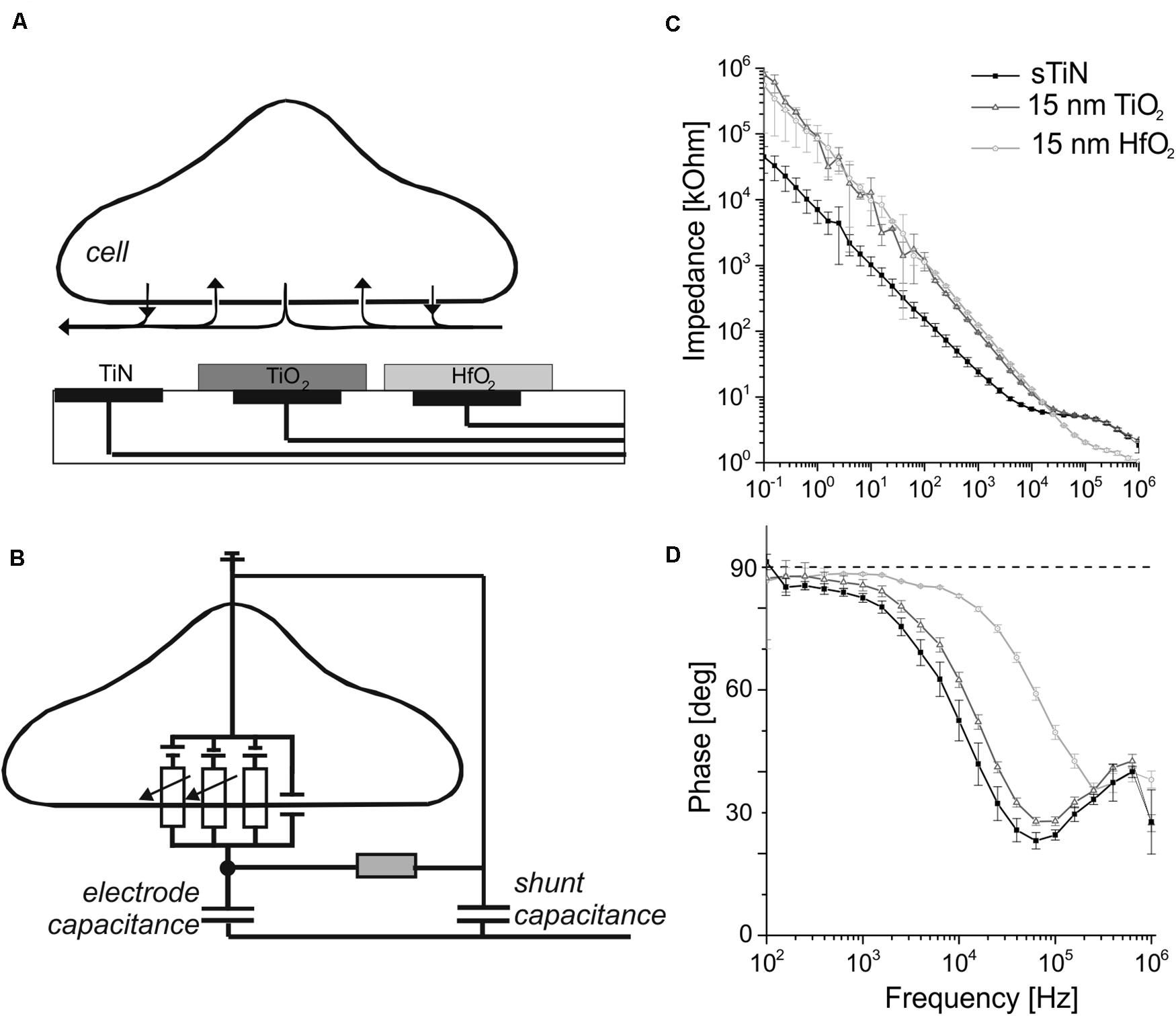
Figure 1. Schematic of the capacitive electrodes used for neural sensing with their impedance and phase behavior. (A) A simplified schematic cross section of the utilized capacitive microelectrode array in contact with an electrogenic cell. Electrodes insulated with ALD-TiO2 or ALD-HfO2 are compared here with bare, compact TiN electrodes. (B) Schematic cross section showing a simplified equivalent circuit of an interfaced electrogenic cell, a capacitive sensing electrode, seal resistance, and shunt capacitance. Figure modified from rf. (Zeck et al., 2017). (C) Impedance measurement of the capacitive electrode with 15 nm TiO2 (dark gray symbols) and 15 nm HfO2 (light gray) and for the uncovered smooth TiN base electrode for comparison (black trace). (D) Phase angle of TiN stimulation electrode covered with 15 nm of HfO2 (light gray) or TiO2 (dark gray). Black symbols denote the phase shift for bare smooth TiN.
The frequency-dependent impedance for electrodes of 1.024 × 10⁻³ cm2 area (square-shaped electrode with 320-μm side length) at frequencies between 100 mHz and 1 MHz is shown in Figure 1C. Electrodes covered with 15-nm ALD-TiO2 and 15-nm ALD-HfO2 were compared to compact, smooth TiN. At 1 kHz, the impedance for smooth TiN electrodes is 24.1 ± 3.46 kΩ (mean ± standard deviation). Upon insulation with TiO2 (15 nm), the impedance increases almost fourfold to 95.5 ± 1.63 kΩ, while upon insulation with HfO2 (15 nm), it increases fivefold to 123.35 ± 2.21 kΩ.
The capacitive property of the electrodes is best visualized using the impedance phase plots (Figure 1D). At 1 kHz, which represents the dominant frequency of single-cell electrical activity, all three electrode types showed a nearly capacitive behavior. The detected phase angle for smooth TiN is 82.5 ± 1.1 degrees, whereas insulation with 15 nm of TiO2 increased the value to 85.6 ± 1.4 degrees. A similarly high value was obtained after insulation with HfO2 (15 nm): 88.3 ± 0.3 degrees. For high frequencies (10 kHz), the phase angle decreases for smooth TiN and for TiO2, but remains at a value of 82.94 ± 0.3 degrees for HfO2.
In summary, the presented electrodes show capacitive behavior up to frequencies of ∼1 kHz for TiN and TiO2 and up to 10 kHz for HfO2. In the following, we measure the specific capacitance of the three electrodes.
Specific Capacitance of TiN Electrodes Coated With ALD Dielectric
The absolute and area-specific values of the electrode capacitance are presented in Figures 2A,B. The absolute capacitance increases linearly with electrode area for all tested ALD oxides. We note that there is a minor offset of 0.2 nF, which we attribute to parasitic capacitances of our measurement setup. This also prevents estimation of the capacitance parameters for small electrodes.
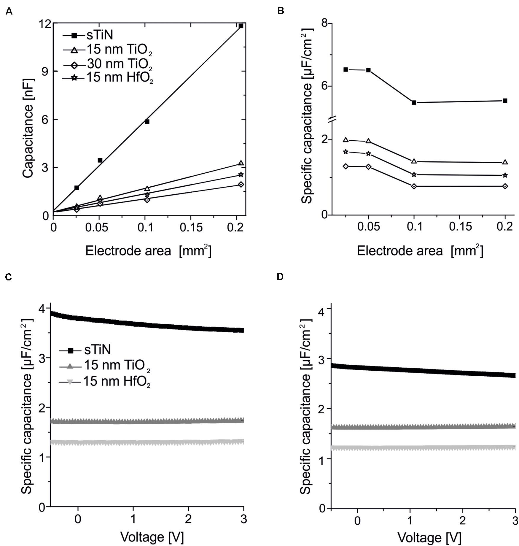
Figure 2. Characterization of the capacitance of the ALD-insulated recording electrodes. (A) Linear dependence of capacitance with electrode area measured using smooth TiN electrodes insulated with 15 or 30 nm of ALD-TiO2, or electrodes insulated with 15 nm ALD-HfO2. The data are compared to uncoated smooth TiN electrodes. Measurements were performed at a frequency of 1 kHz. The linear fit has a small offset (0.2 nF). (B) Specific capacity over area for smooth TiN with 15 or 30 nm of ALD-TiO2, as well as 15 nm ALD-HfO2 compared to the uncoated smooth TiN electrode at a frequency of 1 kHz. (C) Stable behavior of specific capacitance irrespective of the applied DC voltage applied to the electrode. Measurements were performed at 25-Hz stimulation frequency for 15 nm HfO2 (light gray), TiO2 (dark gray) on smooth TiN compared to uncoated TiN electrodes (black line) on large electrodes (320 × 320 μm2). (D) Same analysis as in panel (C) except that here a test frequency of 1 kHz was used.
Results for electrodes with 15 or 30 nm of ALD-TiO2 as well as 15 nm HfO2 are compared to the uncoated TiN electrode. The specific capacitance evaluated for the 15-nm layer of ALD-TiO2 is 1.64 μF/cm2 (estimated from a 0.1-mm2 electrode). This value is slightly higher than that from a literature report for ALD-TiO2 (1.48 μF/cm2) deposited at 300°C on conductive silicon (Wallrapp and Fromherz, 2006). At 30 nm TiO2, both the calculation from impedance measurement and the voltage-dependent direct measurement provide a specific capacitance of 0.99 μF/cm2. This value is higher than the theoretically expected value of 0.82 μF/cm2 if one would assume a linear dependence with oxide thickness. This result suggests that a thin oxide layer may exist between the electrode surface and ALD insulation. The cited literature value refers to remote plasma ALD layers, whereas here with direct plasma ALD is deposited, which results in layers that are more compact and thus a slightly increased capacity. For TiO2, an increasing dependence on capacitance and frequency can be observed when high frequencies are used at high specific capacitances, due to the symmetrical error of the series resistors of the measurement setup (Aarik et al., 2012).
The specific capacitance evaluated for the 15-nm layer of ALD-HfO2 ranges between 1.1 and 1.6 μF/cm2 for the different electrode areas. The range of estimated values (electrode areas: 0.025–0.2 mm2) may be explained by the inaccuracies of electrode sizes used for capacitance estimation. The specific capacitance shows no voltage dependence, i.e., remains stable irrespective of the applied DC electrode voltage (Figure 2C; range = −0.5 to 3 V). The specific capacitance shows little frequency dependence, with a decrease of less than 10% from 25-Hz probing stimulus to a 1-kHz probing stimulus (Figures 2C,D). Further values of the specific capacitance, evaluated at 200 Hz and at 10 kHz, are provided in the Table 1. The shunt capacitance resulting from the insulator covering the conducting pathways and the measurement setup were previously estimated by extrapolation and subtracted.
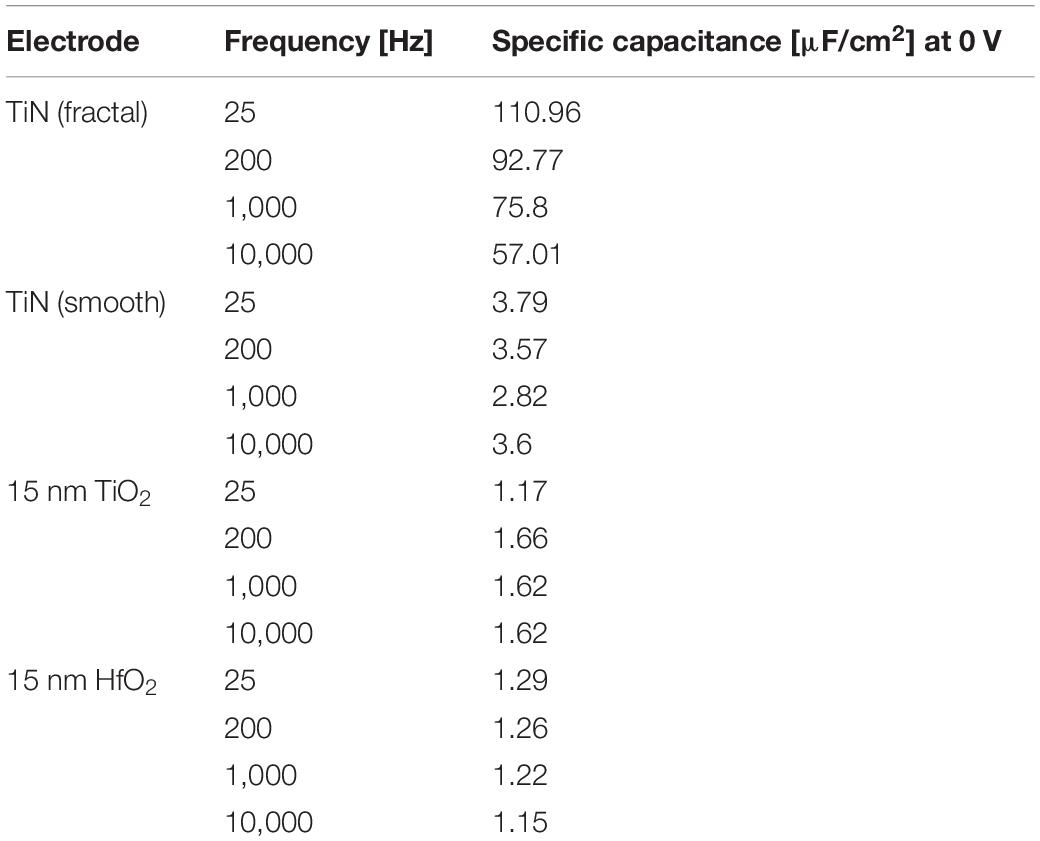
Table 1. Specific capacitance at different frequencies (25 Hz, 200 Hz, 10 kHz, and 10 kHz) for 15 nm HfO2 or TiO2 on smooth TiN electrode (320 × 320 μm2) compared to the specific capacity of uncoated electrodes of both fractal and smooth TiN.
Leakage Current
The leakage current is a second important characteristic of an insulated electrode, as it determines electrode stability. The leakage current density through the dielectric ALD layer of the electrode is shown in Figure 3. A DC voltage (range = +5 V to −3 V) is applied to individual electrodes. Leakage currents are measured for electrodes coated with 15 or 30 nm of TiO2 on smooth TiN, for electrodes coated with 15 nm HfO2 layer, and for electrodes with uncoated smooth TiN electrodes. Both ALD coatings reduce the leakage current over a relatively wide range. The strong increase of the leakage current at bias voltages below −1.8 V might be caused by electrochemical reactions (gas bubble formation) as reported previously (Patan et al., 2006).
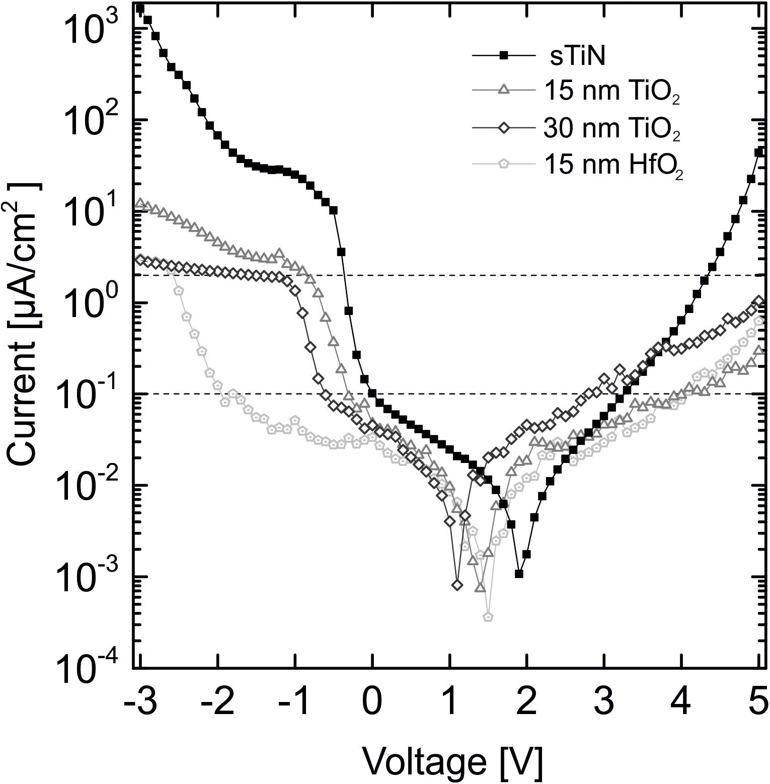
Figure 3. Leakage current behavior of 15 and 30 nm TiO2 on smooth TiN compared to 15 nm HfO2 on TiN and an uncovered TiN electrode at an applied voltage range of +5 V to –3 V. Displayed threshold values of 0.1 μA/cm2 at ±0.8 V [dynamic random access memory (DRAM) applications, International Technology Roadmap for Semiconductors (Aarik et al., 2012)] and the 2 μA/cm2 lowest stimulation threshold limit for cell stimulation (Eickenscheidt et al., 2012).
For the possible application of the characterized stimulation electrodes in neuronal implants, specific threshold values for leakage current density need to be considered. For DRAM applications, a leakage current density of less than 0.1 μA/cm2 [International Technology Roadmap for Semiconductors (ITRS)] in the voltage range ±0.8 V is required (Aarik et al., 2012). Our leakage currents fulfill this requirement. The leakage current minima are shifted because of small offset voltages during measurement, which are not corrected for. If electrodes would be used for electrical stimulation, the leakage current must be below the stimulation threshold limit for activation of electrogenic cells [<2 μA/cm2, (Eickenscheidt et al., 2012)]. The oxides fulfill this requirement up to 4 V as shown by the upper dotted line in Figure 3. The horizontal shift of the minimum values is caused by uncontrolled small potentials at the electrode contact pads.
We summarize that both low-temperature oxides show leakage currents below the required values. Insulation with hafnium oxide is superior to TiO2 with respect to the leakage current.
Electrophysiological Signals From Cardiomyocytes Recorded by ALD-Coated Electrodes
To test the application of electrodes insulated with ALD oxide in electrophysiology, we cultured cardiomyocytes for 5 days (details described in section “Materials and Methods”). Stable and homogenous cultures were obtained on all oxides, as shown in Figures 4A–C. To investigate the biocompatibility of ALD coating, we recorded electrophysiological activity from these cultures. On all MEAs coated with ALD oxides (TiO2 and hafnium oxide, respectively), we recorded electrophysiological activity. We compared the signal shapes and the beating frequency of the cardiomyocyte culture. The signal shapes were qualitatively similar on MEAs coated with oxide as compared to recordings from conventional MEAs for both TiO2 (Figure 4B) and HfO2 (Figure 4C). The smaller signal amplitude is attributed to the signal attenuation by the shunt capacitance across the electrode connecting lead (Figure 1B). The voltage divider between recording electrode impedance (1.5 MOhm at 1 kHz, corresponding to 100 pF) and the shunt capacitance [∼150 pF, (Jones et al., 2020)] reduces the signal amplitude significantly. The beating frequency of the cardiomyocytes recorded on ALD oxide-coated MEAs was the same as the beating frequency recorded on conventional TiN MEAs (data not shown).
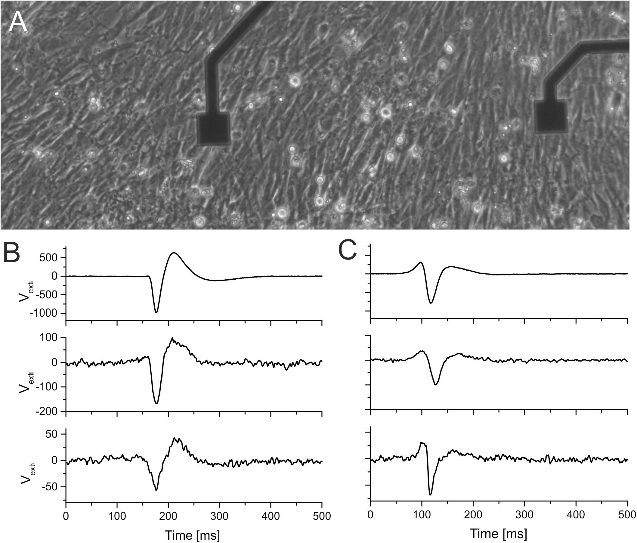
Figure 4. Comparison of signal shapes recorded by TiN electrodes and by insulated (ALD-coated) TiN electrodes. (A) Micrograph of cardiomyocytes grown on HfO2-coated smooth TiN microelectrodes. The electrodes have an edge size of 40 μm. (B,C) Extracellular signals recorded on three different electrodes. The first row in panels (B,C) shows signals recorded using a commercial electrode (fractal TiN). The second row in panels (B,C) shows signals recorded on electrodes where the smooth TiN had been coated with 15 nm of TiO2. The third row shows signals recorded on smooth TiN electrodes coated with HfO2.
Light-Induced Electrophysiological Signals From ex vivo Retina on CMOS-Based MEAs
To demonstrate the benefit of ALD-coated electrodes, we investigated the insulation of CMOS-based MEAs (Bertotti et al., 2014; Thewes et al., 2016 in experiments with ex vivo flat-mount retinal tissues (Figure 5A). If these arrays are coated with sputtered TiO2, they exhibit a strong light dependence, which corresponds to the energy band gap of 3.0 eV (Bertotti et al., 2017). Light-induced physiological retinal activity can be recorded under these conditions for short time periods only (Figure 5B), before driving the sensor in saturation. Here, we therefore coated the CMOS MEAs with hafnium oxide instead of TiO2. Hafnium oxide has an energy band gap of 5.25–5.8 eV (Shaimeev et al., 2007) and is therefore not sensitive to visible light. We first demonstrated the ability of such CMOS MEAs to record light-induced electrophysiological activity from retinal ganglion cells in the explanted ex vivo flat-mounted mouse retina (Figure 5C). Repetitive light pulses (1 Hz) evoke action potentials in retinal ganglion cells, which are detected by the CMO sensors as negative voltage deflections (spikes). Single spikes have the same waveform shape as spikes recorded with TiN electrodes (Figures 4B,C), although with CMOS MEAs, usually larger amplitudes are detected as compared to passive MEAs (Zeck et al., 2017). The CMOS MEA recording electrode (diameter: 8 μm) has a capacitance of about 1 pF (assuming a specific capacitance of 2 μF/cm2). The shunt capacitance for the CMOS MEA has been estimated to be as low as 0.13 pF (Bertotti et al., 2016); therefore, little attenuation is expected. More importantly, hafnium oxide-coated CMOS MEAs exhibit a reduced light sensitivity, which makes them attractive for future applications, including the combination of electrical recording upon strong optogenetic stimulation (Ferrari et al., 2018; Reh et al., 2018).
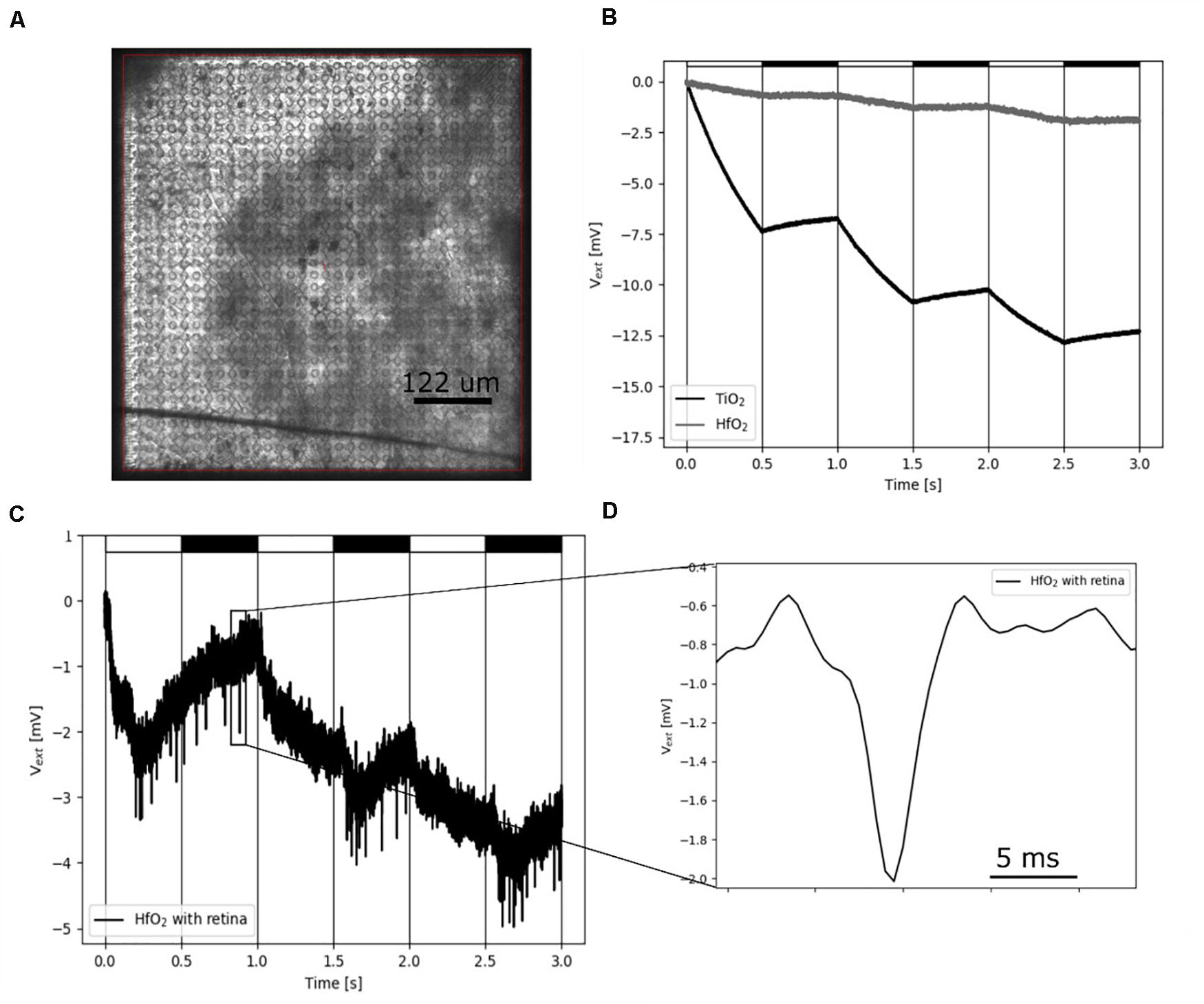
Figure 5. Recording of electrical single-cell activity using hafnium oxide-coated CMOS MEA. (A) Photograph of the CMOS sensor array with interfaced retina. (B) Light-induced drift by illumination using a 460-nm LED on sputtered TiO2 and low-temperature HfO2 ALD-coated CMOS-MEAs. The LED is pulsed with a cycle of 1-Hz, on-off periods represented by white and black rectangles. (C) Low-pass filtered (1.5 kHz) HfO2 ALD-coated CMOS MEA sensor signal. The sensor signal shows spikes of a retinal ganglion cells upon stimulation with 460-nm 1-Hz flicker. (D) Zoom of one single extracellular retinal action potential from panel (C).
Long-Term Biocompatibility of TiN Electrodes Insulated With ALD Oxides
To assess the long-term biocompatibility and biostability of electrodes coated with ALD-TiO2 or with ALD-HfO2 further, we cultured primary neurons for 2–3 weeks (see section “Materials and Methods”). The appearance of neuronal cultures on passive MEAs insulated with ALD- HfO2 was qualitatively indistinguishable from the appearance on control MEAs with commercial, passive MEAs comprising fractal TiN electrodes (Figure 6A).
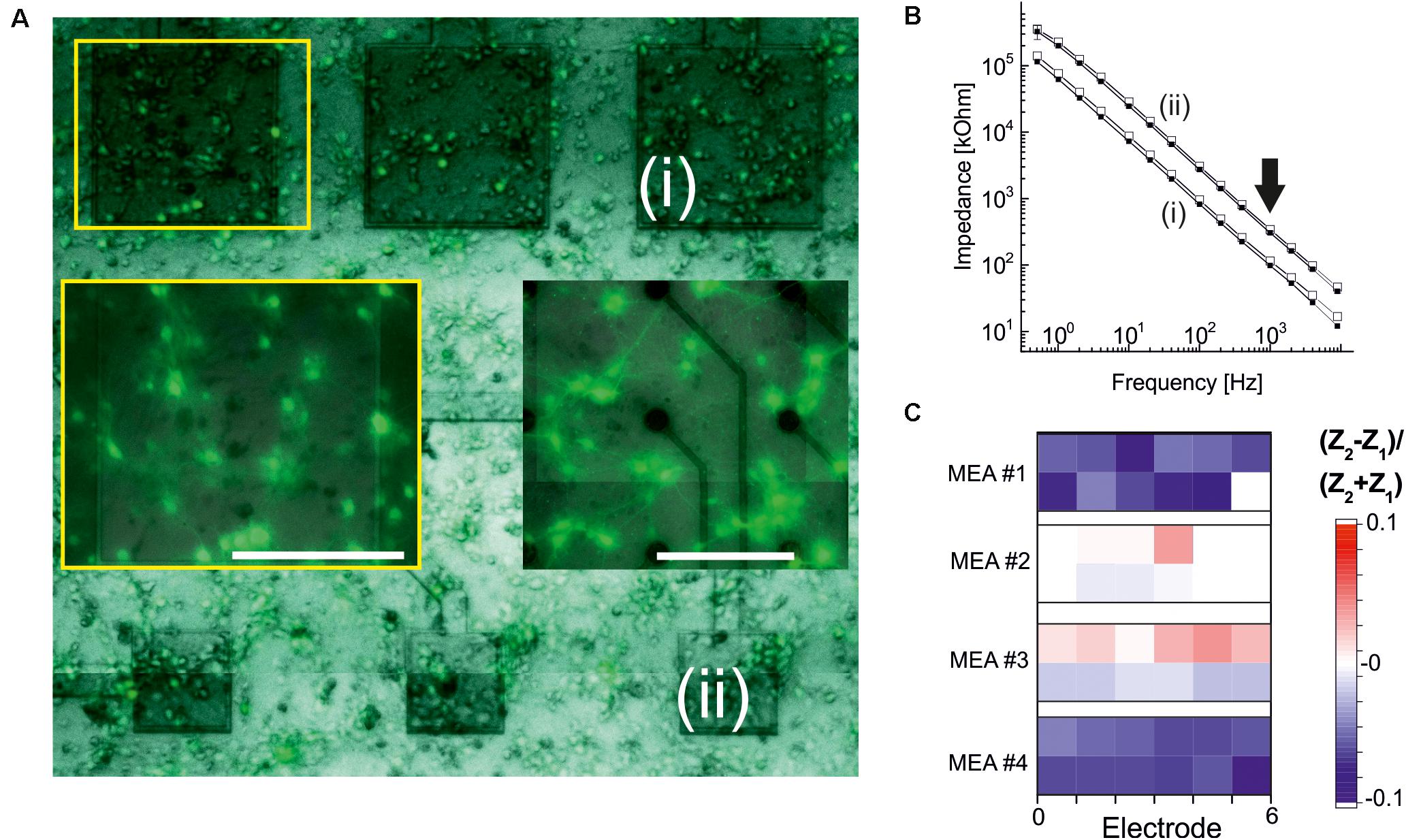
Figure 6. Electrode stability after primary neuronal cultures. (A) Microscopic fluorescence image of an ALD-HfO2-insulated MEA after 2 weeks in culture. Three large electrodes [(i), 320 × 320 μm2; dark gray] and three smaller electrodes [(ii), 160 × 160 μm2] are covered by primary neuronal networks. Left insert marked by yellow rectangle: Fluorescence image at higher magnification showing homogenous networks. Right insert: Fluorescence image of a control culture on a passive MEA with fractal TiN electrodes (Stett et al., 2003). Scale bars: 200 μm. (B) Impedance spectra recorded for the electrodes marked in panel (A). Smaller impedances are recorded for the large electrodes (i). Open symbols denote impedance values before cell culture; filled symbols denote impedance values after cell culture. Arrow indicates toward impedances at 1 kHz. (C) Quantitative evaluation of relative changes in impedance at 1 kHz after cell culture. Blue symbols denote a decrease in impedance; red, an increase. Four MEAs were evaluated, and for each MEA, six large electrodes (320 × 320 μm2; lower row) and six smaller electrodes (160 × 160 μm2) were considered.
To obtain a qualitative assessment of the stability of the ALD oxide-coated electrodes, we measured the impedance of selected electrodes (320 × 320 μm2 and 160 × 160 μm2) prior to neuronal cell culture and after neuronal cell culture. Electrodes were coated either with 15 nm ALD-TiO2 or with 15 nm ALD-HfO2. Example traces of the impedance of two ALD-HfO2 insulated electrode sizes are shown in Figure 6B. We next compared the impedances at 1 kHz, which represents the optimal frequency for recording of neuronal activity. There was a small but significant (p < 0.05, t test) decrease in impedance by 3.7%, calculated for 48 electrodes (Figure 6C) after 14–16 days in culture. In summary, the electrophysiological experiments demonstrate the biocompatibility and biostability of the low-temperature ALD oxides, as well as the benefit for the recording of light-induced neural activity. Future investigations, including in vivo long-term evaluations, are necessary to obtain a conclusive answer about their long-term stability.
Discussion
Here, we investigated the use of low-temperature ALD insulation of TiN electrodes in physiological recordings. Although the coating reduced the electrode capacitance and thus increased its impedance, extracellular action potentials could be reliably recorded on passive MEAs. For CMOS-based MEAs, the small electrode capacitance does not cause signal attenuation because of the even smaller shunt capacitance in the active electrode pixel. We further provided a use case, where ALD oxide protected the light-sensitive CMOS structure and thus enabled improved recording of light-sensitive neural tissue.
Titanium nitride is a conductive electrode material with many advantages. It has a high chemical and mechanical stability, good conductivity, and biocompatibility, as well as a large potential window (Weiland et al., 2002; Cogan, 2008). For in vitro electrophysiology, this material provides good results, and MEAs with TiN electrodes can be reused several times. In vivo TiN electrodes have been used as stimulation electrodes of the subretinal implant Alpha IMS with time to failure of 14.6 months (Daschner et al., 2018). We suggest that for in vivo application, for long-term cell cultures application or for combined optical stimulation and electrical recordings (Kozai and Vazquez, 2015), additional protective layers made of ALD oxides may be used.
We discuss several approaches to improve capacitive electrodes. The large influence of parasitic capacitances on small electrodes represents an obstacle for passive MEAs (Figures 4B,C) but apparently not for CMOS-based MEAs (Figure 5). A possible solution would be to effectively increase the surface area of the electrodes by changing the specific topography without increasing their actual space requirement on the MEA. Approaches to produce three-dimensional structured electrodes and substrates already exist (Heuschkel et al., 2002), but have not been combined with ALD insulation. Optimization of the ALD oxide itself could contribute to an improvement of the capacitive electrode system. For example, the choice of another ALD precursor for TiO2 deposition could positively influence the leakage current behavior of the oxide layer. Here, we used TTIP in combination with O2 plasma, but higher permittivity for layers of TiCl4 precursor with H2O as the second reaction gas (Aarik et al., 2012) has been reported. Adequate doping of TiO2 with aluminum could decrease the leakage current, although the permittivity of the oxide is reduced (Aarik et al., 2012). An O2 plasma pretreatment of the base electrode could positively influence the layer growth by reducing impurities and improving the stoichiometric oxygen ratio at the electrode surface, which would result in a reduction in leakage currents. A final annealing of the oxide layer at 300°C could also reduce leakage current (Fröhlich et al., 2011; Hudec et al., 2011) but may interfere with the goal of low-temperature processing. A reduced shunt capacitance (impedance) of the conducting traces seems indispensable for passive MEAs. This may be achieved by shorter conducting traces and by smaller culture chambers.
Although electrode insulation may enable long-term recording, the reduction of electrode capacitance reduces their use for electrical stimulation. The specific capacitance (∼1–2 μF/cm2) of ALD oxides is too low to be used for efficient electrical microstimulation, which is characterized by stimulus pulses between 0.1 and 5 ms and stimulation charge densities ranging between 0.01 and 1 C/cm2 (Cogan et al., 2016; Corna et al., 2018). Electrodes with fractal surface topography and thus higher active area may be coated with ALD oxides and tested in the future.
ALD oxide coating of microelectrodes may, however, be very beneficial for in vitro recording extending over several months (Odawara et al., 2016) or may be applied to light-sensitive neural recordings, which need to deal with inherent light sensitivity of the recording electrode (El Hady et al., 2013). Specifically, in CMOS-based application, the insulation with CMOS-compatible and light-protecting ALD oxides opens new experimental opportunities. CMOS-based MEAs have lower shunt capacitances compared to the electrode capacitance, and therefore no signal attenuation occurs (Frey et al., 2010; Bertotti et al., 2016). The combination of electrical recording and photostimulation will enable cell type-specific stimulation of optogenetically transduced neurons and simultaneous recording of network activity (Rivnay et al., 2017; Ferrari et al., 2018).
Data Availability Statement
All datasets presented in this study are included in the article/supplementary material.
Author Contributions
VB and GZ designed the study. MD and MR performed the experiments and analyses. MM assisted with ALD oxides. GH was instrumental in processing of the TiN electrodes and MK was in charge for the neuronal culture and Figure 6A. GZ drafted the manuscript with input from all authors. All authors reviewed the final manuscript.
Funding
This work was supported by a grant of the German Ministry of Science and Education (BMBF, FKZ 031L0059A) to MD, MR, GH, MK, and GZ.
Conflict of Interest
The authors declare that the research was conducted in the absence of any commercial or financial relationships that could be construed as a potential conflict of interest.
Acknowledgments
We thank Sandra Buckenmaier and Katja Kuehs for assistance with the cardiomyocyte and primary neuronal cultures, respectively.
References
Aarik, J., Hudec, B., Hušeková, K., Rammula, R., Kasikov, A., Arroval, T., et al. (2012). Atomic layer deposition of high-permittivity TiO2 dielectrics with low leakage current on RuO2 in TiCl4-based processes. Semicond. Sci. Technol. 27:074007. doi: 10.1088/0268-1242/27/7/074007
Andriani, Y., Morrow, I. C., Taran, E., Edwards, G. A., Schiller, T. L., Osman, A. F., et al. (2013). In vitro biostability of poly (dimethyl siloxane/hexamethylene oxide)-based polyurethane/layered silicate nanocomposites. Acta Biomater. 9, 8308–8317. doi: 10.1016/j.actbio.2013.05.021
Barrese, J. C., Aceros, J., and Donoghue, J. P. (2016). Scanning electron microscopy of chronically implanted intracortical microelectrode arrays in non-human primates. J. Neural Eng. 13:026003. doi: 10.1088/1741-2560/13/2/026003
Bertotti, G., Jetter, F., Dodel, N., Keil, S., Boucsein, C., Möller, A., et al. (2016). “Artifact-compensated time-continuous recording from neural tissue during stimulation using a capacitively coupled in-vitro CMOS-MEA with 4k recording and 1k stimulation sites,” in Proceedings of the 2016 IEEE Biomedical Circuits and Systems Conference (BioCAS), Shanghai, 256–259.
Bertotti, G., Jetter, F., Keil, S., Dodel, N., Schreiter, M., Wolansky, D., et al. (2017). Optical stimulation effects on TiO 2 sensor dielectric used in capacitively-coupled high-density CMOS microelectrode array. IEEE Electron Device Lett. 38, 967–970. doi: 10.1109/led.2017.2701901
Bertotti, G., Velychko, D., Dodel, N., Keil, S., Wolansky, D., Tillak, B., et al. (2014). “A CMOS-based sensor array for in-vitro neural tissue interfacing with 4225 recording sites and 1024 stimulation sites,” in Proceedings of the 2014 Biomedical Circuits and Systems Conference (BioCAS), Lausanne, 304–307.
Cogan, S. F. (2008). Neural stimulation and recording electrodes. Annu. Rev. Biomed. Eng. 10, 275–309.
Cogan, S. F., Ludwig, K. A., Welle, C. G., and Takmakov, P. (2016). Tissue damage thresholds during therapeutic electrical stimulation. J. Neural Eng. 13:021001. doi: 10.1088/1741-2560/13/2/021001
Connolly, P., Clark, P., Curtis, A., Dow, J., and Wilkinson, C. (1990). An extracellular microelectrode array for monitoring electrogenic cells in culture. Biosens. Bioelectron. 5, 223–234. doi: 10.1016/0956-5663(90)80011-2
Corna, A., Herrmann, T., and Zeck, G. (2018). Electrode-size dependent thresholds in subretinal neuroprosthetic stimulation. J. Neural Eng. 15:045003. doi: 10.1088/1741-2552/aac1c8
Daschner, R., Rothermel, A., Rudorf, R., Rudorf, S., and Stett, A. (2018). Functionality and performance of the subretinal implant chip Alpha AMS. Sens. Mater. 30, 179–192. doi: 10.18494/sam.2018.1726
Eickenscheidt, M., Jenkner, M., Thewes, R., Fromherz, P., and Zeck, G. (2012). Electrical stimulation of retinal neurons in epiretinal and subretinal configuration using a multicapacitor array. J. Neurophysiol. 107, 2742–2755. doi: 10.1152/jn.00909.2011
El Hady, A., Afshar, G., Bröking, K., Schlüter, O., Geisel, T., Stühmer, W., et al. (2013). Optogenetic stimulation effectively enhances intrinsically generated network synchrony. Front. Neural Circuits 7:167. doi: 10.3389/fncir.2013.00167
Ferrari, U., Deny, S., Sengupta, A., Caplette, R., Sahel, J.-A., Dalkara, D., et al. (2018). Optogenetic vision restoration with high resolution. bioRxiv [Preprint]. doi: 10.1101/470773
Frey, U., Sedivy, J., Heer, F., Pedron, R., Ballini, M., Mueller, J., et al. (2010). Switch-matrix-based high-density microelectrode array in CMOS technology. IEEE J. Solid State Circuits 45, 467–482. doi: 10.1109/jssc.2009.2035196
Fröhlich, K., Hudec, B., Aarik, J., Tarre, A., Machajdík, D., Kasikov, A., et al. (2011). Post-deposition processing and oxygen content of TiO2-based capacitors. Microelectron. Eng. 88, 1525–1528. doi: 10.1016/j.mee.2011.03.129
Fromherz, P. (2002). Electrical interfacing of nerve cells and semiconductor chips. Chemphyschem 3, 276–284. doi: 10.1002/1439-7641(20020315)3:3<276::aid-cphc276>3.0.co;2-a
Gerwig, R., Fuchsberger, K., Schroeppel, B., Link, G. S., Heusel, G., Kraushaar, U., et al. (2012). PEDOT-CNT composite microelectrodes for recording and electrostimulation applications: fabrication, morphology, and electrical properties. Front. Neuroeng. 5:8. doi: 10.3389/fneng.2012.00008
Ghane-Motlagh, B., and Sawan, M. (2013). Design and implementation challenges of microelectrode arrays: a review. Mater. Sci. Appl. 4, 483–495. doi: 10.4236/msa.2013.48059
Heuschkel, M. O., Fejtl, M., Raggenbass, M., Bertrand, D., and Renaud, P. (2002). A three-dimensional multi-electrode array for multi-site stimulation and recording in acute brain slices. J. Neurosci. Methods 114, 135–148. doi: 10.1016/s0165-0270(01)00514-3
Hudec, B., Hušeková, K., Tarre, A., Han, J. H., Han, S., Rosová, A., et al. (2011). Electrical properties of TiO2-based MIM capacitors deposited by TiCl4 and TTIP based atomic layer deposition processes. Microelectron. Eng. 88, 1514–1516. doi: 10.1016/j.mee.2011.03.059
Jalili, R., Kanneganti, A., Romero-Ortega, M. I., and Wallace, G. G. (2017). Implantable electrodes. Curr. Opin. Electrochem. 3, 68–74.
Jones, P. D., Moskalyuk, A., Barthold, C., Gutöhrlein, K., Heusel, G., Schröppel, B., et al. (2020). Low-impedance 3D PEDOT: PSS ultramicroelectrodes. Front. Neurosci. 14:405. doi: 10.3389/fnins.2020.00405
Khodagholy, D., Doublet, T., Gurfinkel, M., Quilichini, P., Ismailova, E., Leleux, P., et al. (2011). Highly conformable conducting polymer electrodes for in vivo recordings. Adv. Mater. 23, H268–H272.
Kozai, T. D., and Vazquez, A. L. (2015). Photoelectric artefact from optogenetics and imaging on microelectrodes and bioelectronics: new challenges and opportunities. J. Mater. Chem. B 3, 4965–4978. doi: 10.1039/c5tb00108k
Kriebel, M., Ebel, J., Battke, F., Griesbach, S., and Volkmer, H. (2020). Interference with complex IV as a model of age-related decline in synaptic connectivity. Front. Mol. Neurosci. 13:43. doi: 10.3389/fnmol.2020.00043
Lao, S. X., Martin, R. M., and Chang, J. P. (2005). Plasma enhanced atomic layer deposition of HfO 2 and ZrO 2 high-k thin films. J. Vac. Sci. Technol. A 23, 488–496.
Marichy, C., Donato, N., Willinger, M. G., Latino, M., Karpinsky, D., Yu, S. H., et al. (2011). Tin dioxide sensing layer grown on tubular nanostructures by a non-aqueous atomic layer deposition process. Adv. Funct. Mater. 21, 658–666. doi: 10.1002/adfm.201001572
Menzler, J., Channappa, L., and Zeck, G. (2014). Rhythmic ganglion cella ctivity in bleached and blind adult mouse retina. PLoS One 9:e106047. doi: 10.1371/journal.pone.0106047
Minton, T. K., Wu, B., Zhang, J., Lindholm, N. F., Abdulagatov, A. I., O’patchen, J., et al. (2010). Protecting polymers in space with atomic layer deposition coatings. ACS Appl. Mater. Interfaces 2, 2515–2520. doi: 10.1021/am100217m
Odawara, A., Katoh, H., Matsuda, N., and Suzuki, I. (2016). Physiological maturation and drug responses of human induced pluripotent stem cell-derived cortical neuronal networks in long-term culture. Sci. Rep. 6:26181.
Patan, M., Shah, T., and Sahin, M. (2006). “Charge injection capacity of TiN electrodes for an extended voltage range,” in Proceedings of the 2006 International Conference of the IEEE Engineering in Medicine and Biology Society, New York, NY, 890–892.
Pimenoff, J. (2012). Atomic layer deposition: excellence in thin film coating. Vak. Forsch. Prax. 24, 10–13. doi: 10.1002/vipr.201200502
Potts, S., Keuning, W., Langereis, E., Dingemans, G., Van De Sanden, M., and Kessels, W. (2010). Low temperature plasma-enhanced atomic layer deposition of metal oxide thin films. J. Electrochem. Soc. 157:66.
Profijt, H., Potts, S., Van De Sanden, M., and Kessels, W. (2011). Plasma-assisted atomic layer deposition: basics, opportunities, and challenges. J. Vac. Sci. Technol. A 29:050801. doi: 10.1116/1.3609974
Ratner, B. D., and Bryant, S. J. (2004). Biomaterials: where we have been and where we are going. Annu. Rev. Biomed. Eng. 6, 41–75.
Reh, M., Kriebel, M., Thewes, R., and Zeck, G. (2018). “Functional characterization of the retinal output upon optogenetic stimulation,” in Proceedings of the 2018 11th International Meeting on Substrate Integrated Microelectrode Arrays MEA Meeting 2018, Reutlingen. doi: 10.3389/conf.fncel.2018.38.00045
Rivnay, J., Wang, H., Fenno, L., Deisseroth, K., and Malliaras, G. G. (2017). Next-generation probes, particles, and proteins for neural interfacing. Sci. Adv. 3:e1601649.
Ryynänen, T., Pelkonen, A., Grigoras, K., Ylivaara, O. M., Hyvärinen, T., Ahopelto, J., et al. (2019). Microelectrode array with transparent ALD TiN electrodes. Front. Neurosci. 13:226. doi: 10.3389/fnins.2019.00226
Schoen, I., and Fromherz, P. (2007). The mechanism of extracellular stimulation of nerve cells on an electrolyte-oxide-semiconductor capacitor. Biophys. J. 92, 1096–1111. doi: 10.1529/biophysj.106.094763
Shaimeev, S., Gritsenko, V., Kukli, K., Wong, H., Lee, E.-H., and Kim, C. (2007). Single band electronic conduction in hafnium oxide prepared by atomic layer deposition. Microelectron. Reliabil. 47, 36–40. doi: 10.1016/j.microrel.2006.03.002
Stett, A., Egert, U., Guenther, E., Hofmann, F., Meyer, T., Nisch, W., et al. (2003). Biological application of microelectrode arrays in drug discovery and basic research. Anal. Bioanal. Chem. 377, 486–495. doi: 10.1007/s00216-003-2149-x
Stutzki, H., Helmhold, F., Eickenscheidt, M., and Zeck, G. (2016). Subretinal electrical stimulation reveals intact network activity in the blind mouse retina. J. Neurophysiol. 116, 1684–1693. doi: 10.1152/jn.01095.2015
Thewes, R., Bertotti, G., Dodel, N., Keil, S., Schröder, S., Boven, K.-H., et al. (2016). “Neural tissue and brain interfacing CMOS devices—An introduction to state-of-the-art, current and future challenges,” in Proceedings of the 2016 IEEE International Symposium on Circuits and Systems (ISCAS), Montreal, 1826–1829.
Wallrapp, F., and Fromherz, P. (2006). TiO[sub 2] and HfO[sub 2] in electrolyte-oxide-silicon configuration for applications in bioelectronics. J. Appl. Phys. 99:114103.
Weiland, J. D., Anderson, D. J., and Humayun, M. S. (2002). In vitro electrical properties for iridium oxide versus titanium nitride stimulating electrodes. IEEE Trans. Biomed. Eng. 49, 1574–1579. doi: 10.1109/tbme.2002.805487
Westerhausen, M., Martin, T., Metzger, M., Blendinger, F., Fleischer, M., Hofmann, B., et al. (2020). Passivated electrode side walls by atomic layer deposition on flexible polyimide based samples. Microelectron. Eng. 227:111315. doi: 10.1016/j.mee.2020.111315
Wissel, K., Brandes, G., Pütz, N., Angrisani, G. L., Thieleke, J., Lenarz, T., et al. (2018). Platinum corrosion products from electrode contacts of human cochlear implants induce cell death in cell culture models. PLoS One 13:e0196649. doi: 10.1371/journal.pone.0196649
Xie, X., Rieth, L., Williams, L., Negi, S., Bhandari, R., Caldwell, R., et al. (2014). Long-term reliability of Al2O3 and Parylene C bilayer encapsulated Utah electrode array based neural interfaces for chronic implantation. J. Neural Eng. 11:026016. doi: 10.1088/1741-2560/11/2/026016
Yin, Z. F., Wu, L., Yang, H. G., and Su, Y. H. (2013). Recent progress in biomedical applications of titanium dioxide. Phys. Chem. Chem. Phys. 15, 4844–4858. doi: 10.1039/c3cp43938k
Keywords: atomic-layer deposition, microelectrode array, neuron, cardiomyocyte, action potential, CMOS MEA
Citation: Dollt M, Reh M, Metzger M, Heusel G, Kriebel M, Bucher V and Zeck G (2020) Low-Temperature Atomic Layer Deposited Oxide on Titanium Nitride Electrodes Enables Culture and Physiological Recording of Electrogenic Cells. Front. Neurosci. 14:552876. doi: 10.3389/fnins.2020.552876
Received: 17 April 2020; Accepted: 13 August 2020;
Published: 18 September 2020.
Edited by:
Jessica O. Winter, The Ohio State University, United StatesReviewed by:
Andreas Offenhäusser, Helmholtz Association of German Research Centres (HZ), GermanyTomi Ryynänen, Tampere University, Finland
Copyright © 2020 Dollt, Reh, Metzger, Heusel, Kriebel, Bucher and Zeck. This is an open-access article distributed under the terms of the Creative Commons Attribution License (CC BY). The use, distribution or reproduction in other forums is permitted, provided the original author(s) and the copyright owner(s) are credited and that the original publication in this journal is cited, in accordance with accepted academic practice. No use, distribution or reproduction is permitted which does not comply with these terms.
*Correspondence: Volker Bucher, dm9sa2VyLmJ1Y2hlckBocy1mdXJ0d2FuZ2VuLmRl; Günther Zeck, Z3VlbnRoZXIuemVja0BubWkuZGU=