- 1Department of Microtechnology and Nanoscience, Chalmers University of Technology, Gothenburg, Sweden
- 2Department of Electrical and Computer Engineering, Texas A&M University-Kingsville, Kingsville, TX, United States
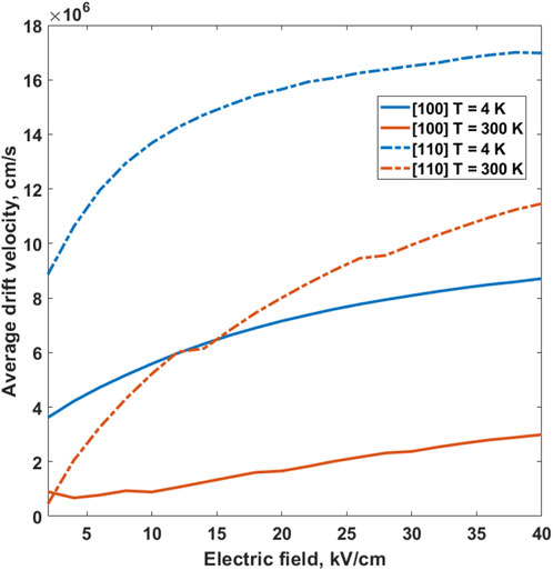
The effects of very low temperature on the electron transport in a [110] and [100] axially aligned unstrained silicon nanowires (SiNWs) are investigated. A combination of semi-empirical 10-orbital tight-binding method, density functional theory and Ensemble Monte Carlo (EMC) methods are used. Both acoustic and optical phonons are included in the electron-phonon scattering rate calculations covering both intra-subband and inter-subband events. A comparison with room temperature (300 K) characteristics shows that for both nanowires, the average electron steady-state drift velocity increases at least 2 times at relatively moderate electric fields and lower temperatures. Furthermore, the average drift velocity in [110] nanowires is 50 percent more than that of [100] nanowires, explained by the difference in their conduction subband effective mass. Transient average electron velocity suggests that there is a pronounced streaming electron motion at low temperature which is attributed to the reduced electron-phonon scattering rates.
1 Introduction
Since the first implementation of top-down Singh et al. (2008) and bottom-up Ma et al. (2003) approaches to fabricate Silicon nanowires (SiNWs), they have constantly shown promising applications in different areas of technology. These are all fueled by the compatibility of their fabrication with the mainstream silicon technology and enhanced quantum mechanical effects as a result of size reduction, e.g., direct bandgap. Tunability of the optical absorption and direct nature of the bandgap bring SiNWs into the photonic realm, for example, photo-detectors, resolving photon polarization Park and Crozier (2015); Zhao et al. (2017), and photovoltaic Gonchar et al. (2019). The surface effects in SiNWs lead to more sensitivity for chemical sensors Kashyap et al. (2022). Breaking the centro-symmetry of the crystal in SiNWs due to strain or surface effects enhances the nonlinear optical effects, e.g., second harmonic generation Wiecha et al. (2015) and third order nonlinear effects Park et al. (2023).
SiNWs have also shown promising benefits in enhancing the coherence of spin-based quantum bits (qubits) as opposed to III-V nanowires in which the coherence of the qubits is limited due to hyperfine magnetic interaction with nuclei. Implementing spin-based qubit chips based on CMOS-compatible SiNW systems are on the rise Zwanenburg et al. (2009); Maurand et al. (2016); Hu et al. (2012); Piot et al. (2022).
Low temperature effects on the charge carrier transport in silicon nanowires also open up new horizons in understandings and possible low-temperature (cryogenic) applications, e.g., CMOS-compatible cryogenic sensors, switches, and deep-space electronics Jones et al. (2020); Rohrbacher et al. (2023). For the latter, the traditionally large bandgap III-V semiconductors are of use despite the high price of their wafer fabrication and processing. SiNWs with direct and controllable bandgap promise a low-cost alternative for III-V counterparts. Different electronic applications of SiNWs are also rising Arjmand et al. (2022); Schmidt et al. (2009), thanks to the developments of CMOS-compatible top-down fabrication methods Singh et al. (2008); Pott et al. (2008). In this article we have studied the effect of low temperature on the transport of electrons at both steady-state and transient conditions under the influence of electron-phonon scattering. The scattering events include both intra- and inter-subband transition processes due to longitudinal acoustic (LA) and longitudinal optical (LO) phonons. Two SiNWs of different crystallographic directions were chosen for the study: a 1.3 nm [110] and a 1.1 nm [100] SiNW, terminated with hydrogen atoms. The band structure data (conduction subbands for electrons) and scattering rates are used by an ensemble Monte Carlo (EMC) code for calculation of electron transport under the influence of applied electric field. The EMC method is a very useful tool to investigate steady-state and transient phenomena in semiconducting nano-devices Tomizawa (1993).
It must be emphasized that in our study, we do not use phenomenological scattering rates or effective mass approximation, rather we calculate the scattering rates ab initio from the band structure information and feed the EMC code with these scattering rates. Reproducing the same experimental observations in SiNWFET Rohrbacher et al. (2023) and CNT Jovanovic and Leburton (1992); Ahmadi et al. (2008), showcase the strength of our model in predicting interesting effects for low-temperature applications. Our method also allows us to monitor how the population of electron is evolving within BZ in response to the applied field. That is a way of designing interesting devices by looking at BZ and determining how to scatter electrons to low mobility subbands and initiate, for example, Gunn effect.
In the next section, we discuss the computational methods including the calculation of band structures, electron-phonon scattering rates and EMC methods. In section 3 we discuss the results. We show that at low temperatures the average drift velocity is enhanced by at least a factor of two due to mitigation of scattering events involving phonon absorption. The difference in the effective mass of [110] and [100] SiNWs leads to better transport (higher electron velocity) in [110] SiNWs. Finally, we show that the initial back-and-forth displacement of electron population in the momentum space, within the first Brillouin zone (BZ), causes streaming motion at moderate bias electric fields. This is supported through transient EMC snapshots of the electron population at different time scales. This effect as well as saturation of drift velocity at higher fields corroborates with previous studies in carbon nanotubes (CNTs) Jovanovic and Leburton (1992); Ahmadi et al. (2008).
2 Computational methods
2.1 Energy minimization and band structure
Two silicon nanowires of different crystallographic directions are investigated here: [110] and [100]. The average diameters for these nanowires are 1.3 nm and 1.1 nm, respectively. The nanowires are considered freestanding, with the surface silicon dangling bonds passivated with hydrogen atoms. Terminating the dangling Si atoms on SiNW is a model for a nanowire surrounded by ideal vacuum or a large-bandgap material or a perfect oxide cladding free of dangling bonds or dislocations. The structural energy of the nanowires is minimized using the density functional theory code in SIESTA. This process allows for the most energetically favorable unit cell to take form and the formation of dangling
The exchange-correlation functional which was used is the Generalized Gradient Approximation (GGA) type with Perdew–Burke–Ernzerhof (PBE) pseudopotentials. The number of

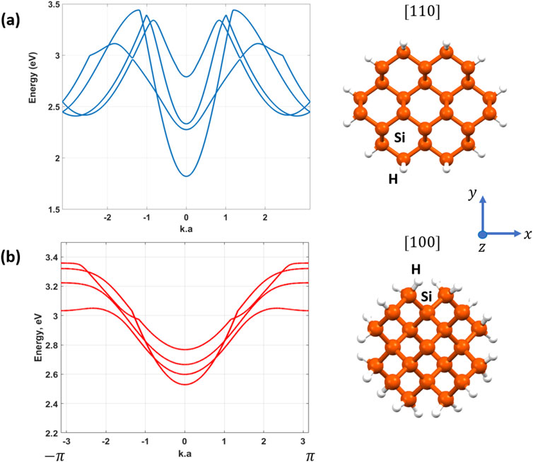
Figure 1. (A) The band structure of 1.3 nm [110] SiNW showing the first four conduction subbands used in the electron-phonon scattering calculation. (B) The band structure showing the first four conduction subbands for 1.1 nm [100] SiNW. The
It was shown that the TB method can faithfully reproduce the experimental data of photoluminescence in silicon nanowires under strain as reported in Walavalkar et al. (2010); Demichel et al. (2011); Bae et al. (2018). As can be seen in Figure 1A, both nanowires are of direct bandgap type. In the [110] SiNW the minimum conduction subband energy is
2.2 Phonon scattering rates and EMC
For the calculation of electron-phonon scattering rates, four first subbands are chosen. The reason for this is to ensure that the energy difference between the minimum conduction energy and the highest one is more than
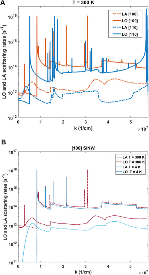
The total scattering rates from the first subband to other bands (the first one included), due to LO and LA phonons for different nanowires and different temperatures are compared in Figure 2. Figure 2A shows the total scattering rates due to LO and LA phonons at room temperature calculated for [100] and [110] nanowires. As can be seen the scattering rates in [100] SiNW are overall higher by a factor of two compared to the [110] SiNW which can be attributed to the effective mass difference of these two nanowire directions as it was shown in Figure 1.

Figure 2. (A) The electron-phonon scattering rates for LA and LO phonons at
This is because the scattering rate depends on the availability of the secondary states quantified by the density of states (DOS). In a 1D solid like nanowire, DOS is proportional to the square root of the effective mass i.e.,
A promising method to scale up the number of superconducting and spin-based qubits, is to co-integrate cryoCMOS control circuits on the same chip instead of relying on many microwave cables from room temperature to the 10 mK stage of dilution refrigerators. The cryoCMOS community is intensively researching on how to model nano-FETs at 4K and below. Therefore we chose 4K as the lower extreme of temperature in this study.
3 Results and discussions
Figure 3 shows the average electron drift velocity as a function of the applied electric field along the length of the nanowires (
where the phonon energy is

Figure 3. The average drift velocity of electron as a function of applied longitudinal electric field for [110] (dashed line) and [100] (solid line) SiNWs at
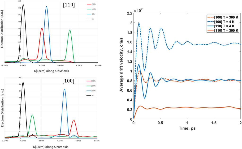
It is also important to look at the transient distribution function in conjunction with the scattering rates in Figure 2. Figure 4 (left panel) depicts the evolving (time-dependent) electron distribution function at

Figure 4. (Left panel, top) Oscillation of electron distribution within the first BZ at a constant electric field
The initial back and forth displacement of electron population in the BZ can be appreciated if we plot the time evolution of average drift velocity which reveals a wealth of information about the scattering mechanism and shows the importance of the peaks in scattering rates through phonon emission. Figure 4 (righ panel) shows the transient average electron drift velocity for the temperatures considered at an electric field of
First, it shows that the velocity is enhanced by decreasing the temperature which is again due to lower scattering rates through phonon absorption at lower temperatures. Second, the streaming motion of electrons, i.e., the ringing of the velocity at initial times becomes more pronounced at lower temperatures, which is also predicted by Jovanovic and Leburton (1992). The streaming motion can be understood through the transient evolution of the electron distribution function (left panel of Figure 4) and scattering rates as shown in Figure 2. The reason for the velocity oscillation in Figure 4 (e.g., from 0 to 600 fs) can be understood if we look at electron distribution inside the first BZ versus time as it was shown in the left panel of Figure 4. The distribution function is seen to ‘bounce’ back and forth. In short, once the electric field is applied, electrons quickly gain crystal momentum and reach the first phonon emission scattering peak. This is where electrons are
It is instructive at this point to discuss the relation between drift velocity and mobility. EMC is an outstanding modeling tool for moderate to high electric fields. At those electric fields, the linear relationship between drift velocity and electric field (the low-field mobility regime or
To manage the required computational resources, we used reasonably small nanowires in this work. However, from a practical point of view, fabrication of small-diameter nanowires i.e., 3 nm diameter, is possible using the top-down CMOS compatible methods Singh et al. (2008). Effect of diameter on the transport depends on the crystallographic direction. We observed previously in Shiri et al. (2018), that for a 3.3 nm [110] SiNW, the direct-indirect energy subband difference is 130 meV (as opposed to 700 meV in Figure 1A for 1.3 nm). As a result of this, at moderate electric fields higher population of electrons ends up in indirect subband with higher effective mass. This leads to lower mobility (current reduction) from which negative differential resistance or Gunn effect results.
4 Conclusion
Using DFT and Ensemble Monte Carlo methods we demonstrated that low temperature has significant effects on electron drift velocity in [110] and [100] silicon nanowires. It was shown that the velocity is enhanced at
Data availability statement
The raw data supporting the conclusions of this article will be made available by the authors, without undue reservation.
Author contributions
DS: Conceptualization, Data curation, Formal Analysis, Investigation, Software, Validation, Visualization, Writing–original draft, Writing–review and editing. RN: Conceptualization, Data curation, Investigation, Resources, Software, Validation, Visualization, Writing–original draft, Writing–review and editing. AV: Conceptualization, Data curation, Formal Analysis, Funding acquisition, Investigation, Resources, Software, Supervision, Validation, Visualization, Writing–original draft, Writing–review and editing.
Funding
The author(s) declare that no financial support was received for the research, authorship, and/or publication of this article.
Acknowledgments
The authors sincerely acknowledge the access to the Stampede2 Supercomputing machine provided by the Texas Advanced Computing Center (TACC) at Austin, United States.
Conflict of interest
The authors declare that the research was conducted in the absence of any commercial or financial relationships that could be construed as a potential conflict of interest.
Publisher’s note
All claims expressed in this article are solely those of the authors and do not necessarily represent those of their affiliated organizations, or those of the publisher, the editors and the reviewers. Any product that may be evaluated in this article, or claim that may be made by its manufacturer, is not guaranteed or endorsed by the publisher.
References
Ahmadi, M. T., Ismail, R., Tan, M. L. P., and Arora, V. K. (2008). The ultimate ballistic drift velocity in carbon nanotubes. J. Nanomater. 2008, 769250. doi:10.1155/2008/769250
Arjmand, T., Legallais, M., Nguyen, T. T. T., Serre, P., Vallejo-Perez, M., Morisot, F., et al. (2022). Functional devices from bottom-up silicon nanowires: a review. Nanomaterials 12, 1043. doi:10.3390/nano12071043
Bae, G., Bae, D.-I., Kang, M., Hwang, S., Kim, S., Seo, B., et al. (2018). “3nm GAA technology featuring multi-bridge-channel FET for low power and high performance applications,” in 2018 IEEE international electron devices meeting (IEDM). doi:10.1109/IEDM.2018.8614629
Buin, A. K., Verma, A., Svizhenko, A., and Anantram, M. P. (2008). Significant enhancement of hole mobility in [110] silicon nanowires compared to electrons and bulk silicon. Nano Lett. 8, 760–765. PMID: 18205425. doi:10.1021/nl0727314
Camenzind, L. C., Geyer, S., Fuhrer, A., Warburton, R. J., Zumbühl, D. M., and Kuhlmann, A. V. (2022). A hole spin qubit in a FIN field-effect transistor above 4 kelvin. Nat. Electron. 5, 178–183. doi:10.1038/s41928-022-00722-0
Demichel, O., Calvo, V., Noé, P., Salem, B., Fazzini, P.-F., Pauc, N., et al. (2011). Quantum confinement effects and strain-induced band-gap energy shifts in core-shell Si-Si nanowires. Phys. Rev. B 83, 245443. doi:10.1103/PhysRevB.83.245443
Gonchar, K. A., Kitaeva, V. Y., Zharik, G. A., Eliseev, A. A., and Osminkina, L. A. (2019). Structural and optical properties of silicon nanowire arrays fabricated by metal assisted chemical etching with ammonium fluoride. Front. Chem. 6, 653. doi:10.3389/fchem.2018.00653
Hu, Y., Kuemmeth, F., Lieber, C. M., and Marcus, C. M. (2012). Hole spin relaxation in Ge–Si core–shell nanowire qubits. Nat. Nanotechnol. 7, 47–50. doi:10.1038/nnano.2011.234
Jacoboni, C., and Lugli, P. (1989). The Monte Carlo method for semiconductor device simulation. Wien: Springer. doi:10.1007/978-3-7091-6963-6
Jancu, J.-M., Scholz, R., Beltram, F., and Bassani, F. (1998). Empirical tight-binding calculation for cubic semiconductors: general method and material parameters. Phys. Rev. B 57, 6493–6507. doi:10.1103/PhysRevB.57.6493
Jones, A. T., Scheller, C. P., Prance, J. R., Kalyoncu, Y. B., Zumbühl, D. M., and Haley, R. P. (2020). Progress in cooling nanoelectronic devices to Ultra-Low temperatures. J. Low Temp. Phys. 201, 772–802. doi:10.1007/s10909-020-02472-9
Jovanovic, D., and Leburton, J. (1992). Electron-phonon interaction and velocity oscillations in quantum wire structures. Superlattices Microstruct. 11, 141–143. doi:10.1016/0749-6036(92)90238-Z
Kashyap, V., Pawar, H., Kumar, C., Chaudhary, N., and Saxena, K. (2022). Analysis of synthesized doped vertical silicon nanowire arrays for effective sensing of nitrogen dioxide: as gas sensors. Front. Mater. 9. doi:10.3389/fmats.2022.1022317
Ma, D. D. D., Lee, C. S., Au, F. C. K., Tong, S. Y., and Lee, S. T. (2003). Small-diameter silicon nanowire surfaces. Science 299, 1874–1877. doi:10.1126/science.1080313
Maurand, R., Jehl, X., Kotekar-Patil, D., Corna, A., Bohuslavskyi, H., Laviéville, R., et al. (2016). A CMOS silicon spin qubit. Nat. Commun. 7, 13575. doi:10.1038/ncomms13575
Park, H., and Crozier, K. B. (2015). Vertically stacked photodetector devices containing silicon nanowires with engineered absorption spectra. ACS Photonics 2, 544–549. doi:10.1021/ph500463r
Park, J.-S., Li, C., Kim, K.-H., Tang, Y., Murphey, C. G. E., Teitsworth, T. S., et al. (2023). Optical nonlinearity in silicon nanowires enabled by bound states in the continuum. ACS Nano 17, 11729–11738. doi:10.1021/acsnano.3c02558
Piot, N., Brun, B., Schmitt, V., Zihlmann, S., Michal, V. P., Apra, A., et al. (2022). A single hole spin with enhanced coherence in natural silicon. Nat. Nanotechnol. 17, 1072–1077. doi:10.1038/s41565-022-01196-z
Pott, V., Moselund, K., Bouvet, D., De Michielis, L., and Ionescu, A. (2008). Fabrication and characterization of gate-all-around silicon nanowires on bulk silicon. IEEE Trans. Nanotechnol. 7, 733–744. doi:10.1109/TNANO.2008.2007215
Rohrbacher, C., Rivard, J., Ritzenthaler, R., Bureau, B., Lupien, C., Mertens, H., et al. (2023). Dual operation of gate-all-around silicon nanowires at cryogenic temperatures: FET and quantum dot. arXiv:2312. doi:10.48550/arXiv.2312.00903
Schmidt, V., Wittemann, J. V., Senz, S., and Gösele, U. (2009). Silicon nanowires: a review on aspects of their growth and their electrical properties. Adv. Mater. 21, 2681–2702. doi:10.1002/adma.200803754
Shiri, D., Verma, A., Nekovei, R., Isacsson, A., Selvakumar, C. R., and Anantram, M. P. (2018). Gunn-Hilsum effect in mechanically strained silicon nanowires: tunable negative differential resistance. Sci. Rep. 8, 6273. doi:10.1038/s41598-018-24387-y
Singh, N., Buddharaju, K. D., Manhas, S. K., Agarwal, A., Rustagi, S. C., Lo, G. Q., et al. (2008). Si, SiGe nanowire devices by top–down technology and their applications. IEEE Trans. Electron Devices 55, 3107–3118. doi:10.1109/TED.2008.2005154
Soler, J. M., Artacho, E., Gale, J. D., García, A., Junquera, J., Ordejón, P., et al. (2002). The SIESTA method for ab initio order-N materials simulation. J. Phys. Condens. Matter 14, 2745–2779. doi:10.1088/0953-8984/14/11/302
Verma, A., Buin, A. K., and Anantram, M. P. (2009). High-field hole transport in silicon nanowires. J. Appl. Phys. 106, 113713. doi:10.1063/1.3264629
Verma, A., Shiri, D., and Nekovei, R. (2023). “Low-temperature effects on electron transport in small-diameter silicon nanowire,” in 2023 IEEE nanotechnology materials and devices conference (NMDC), 31–34. doi:10.1109/NMDC57951.2023.10343599
Walavalkar, S. S., Hofmann, C. E., Homyk, A. P., Henry, M. D., Atwater, H. A., and Scherer, A. (2010). Tunable visible and near-IR emission from sub-10 nm etched single-crystal Si nanopillars. Nano Lett. 10, 4423–4428. PMID: 20919695. doi:10.1021/nl102140k
Wiecha, P. R., Arbouet, A., Kallel, H., Periwal, P., Baron, T., and Paillard, V. (2015). Enhanced nonlinear optical response from individual silicon nanowires. Phys. Rev. B 91, 121416. doi:10.1103/PhysRevB.91.121416
Zhao, X., Alizadeh, M. H., and Reinhard, B. M. (2017). Generating optical birefringence and chirality in silicon nanowire dimers. ACS Photonics 4, 2265–2273. doi:10.1021/acsphotonics.7b00501
Keywords: silicon nanowire, cryogenic, electron-phonon scattering, DFT, ensemble Monte Carlo, CMOS, spin qubit
Citation: Shiri D, Nekovei R and Verma A (2024) Low-temperature electron transport in [110] and [100] silicon nanowires: a DFT-Monte Carlo study. Front. Nanotechnol. 6:1494814. doi: 10.3389/fnano.2024.1494814
Received: 16 September 2024; Accepted: 06 November 2024;
Published: 20 November 2024.
Edited by:
Alexandre Reily Rocha, São Paulo State University, BrazilReviewed by:
Mykhailo V. Klymenko, RMIT University, AustraliaNguyen Van Toan, Tohoku University, Japan
Copyright © 2024 Shiri, Nekovei and Verma. This is an open-access article distributed under the terms of the Creative Commons Attribution License (CC BY). The use, distribution or reproduction in other forums is permitted, provided the original author(s) and the copyright owner(s) are credited and that the original publication in this journal is cited, in accordance with accepted academic practice. No use, distribution or reproduction is permitted which does not comply with these terms.
*Correspondence: Daryoush Shiri, c2hpcmlAY2hhbG1lcnMuc2U=
 Daryoush Shiri
 Reza Nekovei2
 Amit Verma