 Bernice Mae Yu Jeco-Espaldon
 Wipakorn Jevasuwan
 Yoshitaka Okada
 Naoki Fukata
- 1Research Center for Materials Nanoarchitectonics (MANA), National Institute for Materials Science (NIMS), Tsukuba, Japan
- 2Center for Advanced New Materials, Engineering, and Emerging Technologies (CANMEET), University of San Agustin, Iloilo, Philippines
- 3Department of Electronics Engineering, College of Technology, University of San Agustin, Iloilo, Philippines
- 4Research Center for Advanced Science and Technology (RCAST), The University of Tokyo, Tokyo, Japan
Nanostructured silicon solar cells are designed to minimize costs through reduced material usage while enhancing power conversion efficiency via superior light trapping and shorter charge separation distances compared to traditional planar cells. This study identifies the optimal conditions for nanoimprinted silicon nanowire (SiNW) solar cells to achieve maximum efficiency under low sunlight concentration and evaluates their performance as bottom cells in III–V multijunction solar cell systems. The findings indicate that the SiNW solar cell reaches its peak performance at a concentration factor of 7.5 suns and a temperature of 40°C or lower. Specifically, the absolute conversion efficiency under these conditions is 1.05% higher than that under unconcentrated light. Compared to a planar silicon solar cell under identical conditions, the SiNW solar cell exhibits a 3.75% increase in conversion efficiency. Additionally, the SiNW single-junction solar cell, when integrated in series with a commercial lattice-matched InGaP/GaAs dual-junction solar cell, was tested under unconcentrated sunlight, specifically at one-sun, global air mass 1.5 condition, to assess its viability in one-sun multi-junction solar cell applications. The results suggest that a III–V upper subcell with a smaller active area than that of the SiNW subcell is optimal for maximizing current production, which is favorable to the cost reduction of the device. This hybrid configuration is particularly advantageous for terrestrial applications, such as electric vehicles, which demand lightweight, high-performance multijunction solar cell devices. Although the weight reduction of the characterized SiNW solar cell with a full silicon substrate compared to its planar solar cell counterpart is 1.8%, recommendations to increase this reduction to as much as 64.5% are discussed to conclude this paper.
1 Introduction
Silicon photovoltaics (Si PV) represent by far the most developed and widely explored solar cell technology. The highest solar cell efficiencies garnered were approximately 27% (Yoshikawa et al., 2017; Slade and Garboushian, 2005), while the Shockley–Queisser (SQ) efficiency limit for a 1.1 eV single-junction Si solar cell was calculated to be approximately 32% (Rühle, 2016). With these, key technologies are being explored and technical challenges are being addressed to finally reach or even exceed the SQ efficiency limit. There are fundamental reasons why this efficiency limit is difficult to reach, although the Si PV technology is considered mature. One reason is the angle mismatch and temperature differences between the photon absorption and emission of the solar cell material, also known as Boltzmann loss (Hirst and Ekins-Daukes, 2011). In addition, a planar Si solar cell absorber typically allows only one photon excitation and requires longer carrier lifetimes as compared with its low-dimensional structure counterparts. A potential solution to this is the use of nanostructured solar cells. Nanostructured solar cells, like Si nanowires (SiNWs), allow multiple exciton generation (MEG), which then increases carrier generation available for collection (Fukata et al., 2017). Although the first versions of SiNW solar cells achieved an efficiency of less than 1% (Tsakalakos et al., 2007; Stelzner et al., 2008), as of this article, multiple studies have already explored how to optimize SiNW solar cells (Kumar et al., 2011; Huang et al., 2012; Jung et al., 2013). SiNW solar cells, when designed with periodicity on the same order as the photon wavelength, can demonstrate high light-trapping efficiencies (Garnett and Yang, 2010; Yu et al., 2016), thereby allowing more photons to excite electrons in the conduction band and produce current. Another possible way is to concentrate sunlight on the Si absorber. Although there have been studies on planar Si single junction solar cells (1JSCs) (Yoshikawa et al., 2017; Campbell and Green, 1986; Sinton and Swanson, 1987; Xing et al., 2015; Sinton et al., 1986; Green et al., 1986), there are no studies yet on SiNW 1JSCs for concentrator systems to the best of the authors’ knowledge. Such studies were probably unpursued due to the unwanted effects of Auger recombination at high temperatures brought about by long exposure to high solar irradiance (Vossier et al., 2010).
Currently, the highest solar cell efficiency is achieved by multijunction solar cells (MJSCs) made entirely of III–V compound semiconductors, reaching an efficiency of 47.6% under a sunlight concentration of 665 suns (Fraunhofer Institute for Solar Energy Systems, 2022), where 1 sun is 100 mW/cm2. Despite their superior performance, these cells are prone to thermal runaway over time (Zimmermann, 2013; Bett and Yarema, 2022; Nakamura et al., 2023; Algora, 2007), which can significantly reduce their lifespan. Additionally, the limited availability of group III materials poses substantial challenges for their widespread commercialization (Fitchette and Freundlich, 2016). To address these issues, replacing the long-wavelength absorber with a more cost-effective material, such as silicon, in concentrator III–V-based MJSCs could lower the overall cost of this technology. Although III–V on planar Si MJSCs have been extensively studied for terrestrial applications (Yamaguchi et al., 2024; Essig et al., 2017; Schygulla et al., 2022), the current record efficiency for these devices is held by wafer-bonded, two-terminal III–V//Si triple-junction solar cells (3JSCs), which have achieved an efficiency of 36.1% under concentrated sunlight conditions (Schygulla et al., 2023). Although there are several studies already on nanostructured III–V on Si MJSCs (Tong, 2023; Mi and Chang, 2009; Zhao et al., 2008), specific studies on III-V on nanostructured Si MJSCs have no publications to date with no studies published to date. Meanwhile, perovskite-on-Si tandem solar cells have demonstrated efficiencies (Liu et al., 2023) of approximately 34%. Despite their promising performance, these cells are susceptible to degradation under prolonged sunlight exposure, which can lead to phase changes in the perovskite layer. This vulnerability raises concerns about their performance stability, particularly when exposed to concentrated sunlight over extended periods, where the degradation may be accelerated (Azkar Ul et al., 2024; Deng et al., 2018; Hou et al., 2020; Schulze et al., 2020; Köhnen et al., 2021).
From the gaps identified, it may be worth exploring at which amount of sunlight concentration (in suns) will the SiNW solar cells deliver the optimal efficiency and determine their suitability as bottom cells for III–V-based MJSCs. Hence, we explored the performance of nanoimprinted SiNW solar cells at sunlight concentration factors between 1 and 20 suns and at various cell operating temperatures between 25°C and 100°C. Investigating these effects is critical for optimizing solar cell designs for real-world applications, particularly in varying environmental conditions. Additionally, we obtained the current–voltage (J-V) characteristics of an SiNW 1JSC electrically connected to a commercial lattice-matched (LM) InGaP/GaAs dual-junction solar cell (2JSC) to determine the performance of the SiNW as a bottom cell for III–V-based MJSCs. This was explored to leverage the high efficiency of III–V cells while potentially reducing costs through the use of SiNW technology. This hybrid approach is particularly relevant for terrestrial applications, such as electric vehicles, where cost-effective and efficient energy solutions are increasingly necessary (Yamaguchi et al., 2021; Stauch, 2021; Alanazi, 2023).
2 Materials and methods
2.1 SiNW nanoimprint on 2” (100) n-Si wafers
SiNWs on a 2″ n-type Si (100) substrates were fabricated by nanoimprinting, followed by the Bosch process, as done by Jevasuwan et al. (2016), with some modifications. First, a 300-nm-thick commercial photoresist (NIAC) was spin-coated onto the samples at 4,000 rpm for 60 s. Following the spin-coating, the samples were baked at 70°C for 20 s to ensure that the photoresist was adequately dried. Next, a 30-nm-thick magnesium oxide (MgO) layer was deposited on the photoresist. This layer serves as a mask for the subsequent patterning of the nanowires. The patterning was achieved using UV nanoimprint lithography, employing a circular mask file to define the desired features. The 30-nm-thick MgO layer provides sufficient coverage for effective masking during the imprinting process. After imprinting, the wafers were baked for 5 min. Next, the photoresist was lifted off using an N-methyl-2-pyrrolidone (NMP) solution. After this, the wafers with the nanoimprinted wires were subjected to the Bosch process. Specifically, this step employed deep Si etching for 3 min using SF6 and C4F8 plasma. These gases were kept at a flow rate of 35 sccm under 0.75 Pa. The RF power of the plasma was set at 100 W. The etching depth was confirmed after deep Si etching using scanning electron microscopy (SEM). Finally, the 30-nm MgO layer was etched out using a 1% H3PO4 solution. The process flow of the SiNW nanoimprinting lithography described is shown in Figure 1. The SiNW pitch and height are both 500 nm, and the diameter is 200 nm, as illustrated in Figure 2A, and the arrays of SiNW viewed in SEM are shown in Figure 2B.
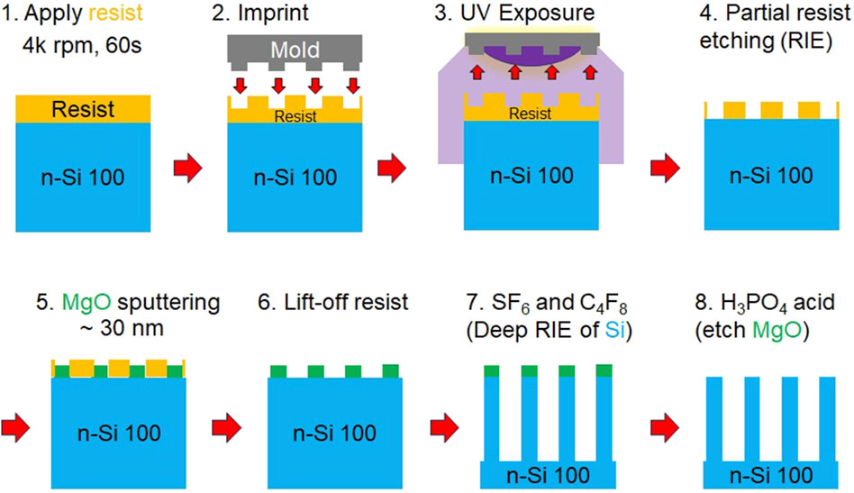
Figure 1. Process flow diagram of SiNW nanoimprinting lithography.
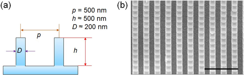
Figure 2. (A) Cross-section illustration (not to scale) of SiNWs with dimensions indicated. (B) Tilted (30°) cross-section SEM image of nanoimprinted SiNWs before junction growth viewed at 25.0 k magnification, 10.0 kV. The scale bar is 2.00 µm.
2.2 SiNW solar cell fabrication
After nanoimprinting the SiNW on n-Si substrates, solar cell fabrication was done as follows. First, the samples were cut into a size of 15 mm × 15 mm and then pre-treated with 2% hydrofluoric (HF) acid for 90 s. Next, the junction was grown by chemical vapor deposition (CVD) at 750°C for 3 min, while SiH4 and B2H6 gases were flown at 19 and 0.5 sccm, respectively. The thickness of the p-type Si in this condition was approximately 70 nm. The back surface underwent dry etching for 40 min using SF6 gas at a flow rate of 20 sccm. Then, the samples were treated with 2% HF acid for 60 s. The back surface was spin-coated with a p-dopant solution at 5,000 rpm for 60 s. The samples with back surface p-dopant were then subjected to thermal annealing at 850°C for 25 min to allow phosphorus diffusion. After this, the samples were treated with 5% HF acid for 2 min to remove the residual dopant solution at the backside and reduce surface oxides. Next, the Ti/Ag back contact multilayer was deposited by reactive sputtering. The Ti layer was deposited at an RF power of 200 W for 16 min, while the Ag layer was deposited at a DC power of 170 W for 4 min. These back electrode layers were grown to a size of 50 nm and 200 nm, respectively. Both steps were done while 15 sccm Ar gas was flowing in the sputter chamber. Then, on the front side, a 250-nm Ag layer was deposited by reactive sputtering at a DC power of 170 W for 4 min, and Ar gas was also flown at 15 sccm. A stainless-steel mask (SUS304) was used to selectively deposit the front electrode pattern. Finally, an approximately 120-nm-thick indium–tin oxide (ITO) layer was deposited on the front surface of the device by reactive sputtering. The sputtering process was carried out at an RF power of 100 W for approximately 14 min. During the deposition, Ar and O2 gases were introduced into the sputtering chamber at flow rates of 19.2 sccm and 0.8 sccm, respectively. The ITO layer serves as a transparent conductive electrode that aims to enhance carrier collection from the device. The same process was used for fabricating the planar Si solar cells. The simplified cross-section schematics of the solar cells are shown in Figure 3.
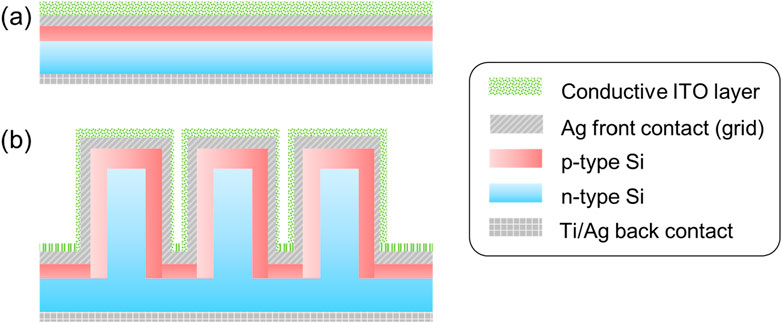
Figure 3. Cross-section schematic illustration of (A) planar Si and (B) SiNW solar cells.
After ITO layer sputtering, the samples were manually cut with a diamond pen within the spans of the front electrode’s busbars and grid. Thus, the effective active area of each sample was expected to be different. The effective cell areas were determined by the ratio and proportion of the cell’s short-circuit current, ISC, in amperes with and without a 0.16-cm2 mask on the cell during measurement. The measured effective active areas of the best planar Si and SiNW solar cell samples were 0.33 and 0.43 cm2, respectively.
2.3 Optoelectronic characterization
2.3.1 Current–voltage (J–V) characteristic measurements
The DC J–V characteristic measurements were acquired from planar Si and SiNW solar cells. There were two setups used for these measurements. One was a continuous 150-W Xe white bias lamp (Bunkoukeiki Co., Ltd.) simulating the 1-sun, global air mass 1.5 (AM 1.5G) standard condition. It has an illumination area of 20 mm × 20 mm, JIS C8912/C8933 class A spectral match, and a non-uniformity irradiance of ±5%. Its light intensity stability is within ±3%. On the other hand, the pulsed J–V measurement setup that simulates variable sunlight concentration factors employed a flash lighting system (Sugawara Laboratories Inc.: ESD-VF2M-U2 strobe driver and SLA-153-U1 lamp housing). The flash lamp’s flashing range, duration, and delay time are 0.22 Hz, 50 µs to 2 m, and 10 µs, respectively. Both lamps were irradiated through AM 1.5 G filters and were calibrated with a commercial crystalline Si photodetector diode with known 1-sun current production (Bunkokeiki, 2012).
Right after electrode fabrication, the 1-sun J–V characteristics of the planar Si and SiNW solar cells were measured at room temperature using the continuous lamp. Then, prior to pulsed J–V characteristic curve measurements, the back contacts of the bare cells were mounted on different Cu plates using In paste at 180°C. After cooling down, the front electrodes were bonded using the Al wire to the other side of the Cu plate, which is electrically isolated from where the back contact was mounted. The actual images of the mounted samples are shown in Supplementary Figure S1. The pulsed J–V curves were obtained at various concentration factors between 1 and 20 suns. Using a Peltier stage, pulse measurements were also obtained at various cell temperatures between 25°C and 100°C.
We also measured the current–voltage characteristic curves from the p-on-n SiNW 1JSC using an InGaP/GaAs 2J filter, a commercial n-on-p InGaP/GaAs 2JSC and series-connected commercial n-on-p InGaP/GaAs 2JSC and SiNW 1JSC we fabricated to emulate a three-terminal, triple-junction solar cell (3JSC), hereby referred to as InGaP/GaAs//SiNW 3JSC. The series-connected InGaP/GaAs//SiNW 3JSC was measured using two independent, AM 1.5G 1-sun calibrated solar simulators. A schematic of the dual lamp setup is shown in Figure 4.
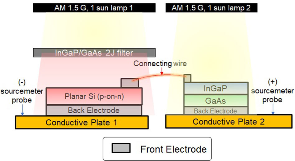
Figure 4. Schematic illustration of dual AM 1.5G, 1-sun-calibrated lamp setup for measuring the J–V characteristics of InGaP/GaAs//SiNW 3JSC. The measured InGaP/GaAs 2JSC is an n-on-p device, while the series-connected SiNW 1JSC is a p-on-n device.
The series resistance, RS, and shunt resistance, RSH, were approximated using
where Vu+1 and Vu are adjacent voltages; Ju+1 and Ju are the adjacent current densities corresponding to Vu+1 and Vu, respectively; and w is the total number of data points within the voltage range chosen. The voltage ranges used in RS and RSH calculations were from VOC to VOC + 0.04 V and from 0 to 0.2 V, respectively, in which these parasitic resistances are most pronounced.
2.3.2 External quantum efficiency measurements
External quantum efficiency (EQE) measurements were obtained to quantify the photon-to-electron conversion of the planar Si and nanoimprinted SiNW solar cells. A chopped monochromated light was used to illuminate the samples during measurements. The monochromated light sources are 500-W Xe and 400-W halogen lamps calibrated at AM 1.5G conditions using a crystalline Si photodetector diode with known 1-sun current production (Bunkokeiki, 2012). The lamps have JIS C8912/C8933 Class A standard spectral match, irradiation intensities of 5–50 μW/cm2 between 300 and 1,200 nm, positional non-uniformity of within ±2.5%, wavelength intensity constancy within ±3%, and a maximum wavelength variability of 20 nm. The illumination area is within 20 mm × 20 mm. Using a Peltier stage, EQE measurements at various cell temperatures were carried out. The measurements were acquired at short-circuit conditions, i.e., at V = 0 V. Then, the current density was derived using the relation
where
2.3.3 Laser beam-induced current mapping
One can employ laser beam-induced current (LBIC) mapping to observe the quality of the cell’s active area (Bajaj et al., 1987; Honsberg and Bowden, 2010) and quantify its current production uniformity. In this work, a modulated 785-nm laser was used to excite the Si solar cells. Modulating a laser enables enhanced signal-to-noise ratio (SNR) and improved spatial resolution, which results in better quality of LBIC map images. The measured laser power density, switching frequency, scanning frequency, and duty cycle of the laser are 3,550 mW/cm2, 2000 Hz, 2 Hz, and 50%, respectively. The Peltier stage was also used to vary the cell operating temperature between 25°C and 100°C (Yu Jeco et al., 2019a; Yu Jeco et al., 2018a).
To quantify the homogeneity of carrier collection, the current uniformity was calculated using standard deviation,
where
3 Results and discussion
3.1 Planar Si and SiNW 1JSCs at 1-sun, room temperature
3.1.1 J–V characteristic curve
The J–V characteristic curves of planar Si and SiNW solar cells were measured to determine their electrical performance in pristine conditions, particularly after ITO layer deposition. Figure 5 shows the J–V characteristic curves of the best-performing planar Si and SiNW solar cells at 1-sun, AM 1.5G, room temperature condition. The electrical parameters of the solar cells derived from 1-sun J–V characteristic curves are listed in Table 1. By visual inspection, it can be inferred that the performance of the SiNW solar cell is better than that of the planar Si solar cell. Such inference is reflected numerically in their short-circuit currents, JSC, open-circuit voltages, VOC, and conversion efficiencies, η. Approximately 4.1% higher η than the η of the planar structure was achieved using the SiNW structure for solar cells. However, the fill factor (FF) of SiNW is less than the FF of the planar Si solar cell. This is attributed to the SiNW solar cell having a significantly larger JSC than planar Si while having a small difference in VOC. The reason the VOC of the SiNW 1JSC did not increase significantly compared to the VOC of the planar Si 1JSC can be explained as follows. Their energy gaps, E.g., did not vary because the NW height (500 nm) and diameter (200 nm) are still too high to induce the quantum confinement effect. In past literature, the NW diameter, dNW, that can cause a noticeable increase in E.g., should be in the range of 1–10 nm (Xia and Cheah, 1997; Li and Wang, 2004). Using the relation between the change in E.g., ΔEg, and dNW (Li and Wang, 2004), we have
where βNW and αNW for Si were empirically determined to be 1.53 and the unit of βNW is eV × (nm)α; the estimated
A 0.46 meV increase in E.g., does not significantly change VOC as it would if dNW is approximately 1–10 nm. If dNW was either 1 nm or 10 nm, ΔEg would have been 1.53 eV and 45.2 meV, respectively.
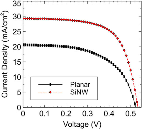
Figure 5. One-sun, AM 1.5G J–V characteristic measurements obtained from planar Si and SiNW 1JSCs after ITO layer deposition.
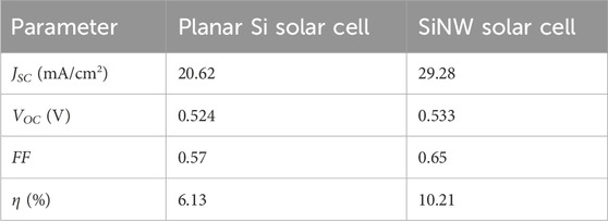
Table 1. Planar Si and SiNW solar cell performance at 1-sun, AM 1.5G illumination, and room temperature.
3.1.2 EQE measurements
EQE measurements were obtained from Cu-mounted planar and SiNW 1JSC. Figure 6 shows the EQE response of the solar cells. Between 350 and 450 nm, the EQE response of the planar Si solar cell was higher than that of the SiNW. Since the SiNW has a larger surface area than planar Si, more surface defects may form, thereby degrading the EQE response at shorter wavelengths. On the other hand, beyond 450 nm, the EQE response of the SiNW solar cell is much higher than that of the planar Si solar cell. Surface recombination has less impact on longer wavelengths as they are absorbed deeper in the bulk silicon, away from the surface defects. Carriers generated deeper in the bulk by longer wavelengths have a higher probability of being collected despite surface defects (Oh et al., 2012). One way to mitigate this is to coat the SiNW with Ir(III). Our device did not have an Ir(III) coating (Kim et al., 2018); hence, compared with the planar 1JSC, the light-to-electricity conversion in SiNW 1JSC was only improved from 450 nm and beyond.
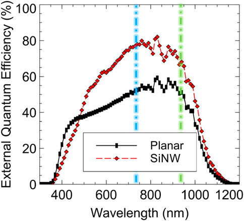
Figure 6. EQE measurements obtained from planar Si and SiNW solar cells at room temperature. The dashed–dotted lines are placed at 670 nm (≈Eg,InGaP = 1.87 eV) and 870 nm (≈Eg,GaAs = 1.42 eV).
As for the potential use of the SiNW as a lower-bandgap subcell in an MJSC device, one must select an upper subcell that will enable the SiNW subcell to absorb wavelengths beyond 450 nm. To explore this further, the JSC values at two wavelength ranges were derived from the EQE measurements. The ranges of 670–1,200 nm and 870–1,200 nm were chosen to determine how much JSC the SiNW subcell may produce when stacked with InGaP only and InGaP/GaAs absorbers, respectively. These materials are typically used as upper subcells of III–V-based MJSCs (Cotal et al., 2009), where the bandgaps of InGaP and GaAs are 1.87 and 1.42 eV (Kazuaki and Takaaki, 2011), corresponding to absorption band edges of approximately 670 nm and 870 nm, respectively. The calculated JSC values from EQE at different wavelength ranges using Equation 2 are summarized in Table 2. Based on the calculated JSC values, the currents required for matching the SiNW as a bottom cell with an InGaP top cell and an InGaP/GaAs 2J tandem cell are approximately 15.74 and 5.40 mA/cm2, respectively. Practically, the JSC of III–V-based individual and tandem cells is approximately 10–14 mA/cm2 at 1 sun (Cotal et al., 2009; Takamoto et al., 2005; Lueck et al., 2006). Thus, the estimated current mismatch for InGaP and InGaP/GaAs on SiNW systems would be 1.74–5.74 mA/cm2 and 4.6–8.6 mA/cm2, respectively. Nevertheless, there are possible approaches to augment this issue. The simplest approach would be to implement a three-terminal configuration in which a third conductive electrode is placed between the III–V and the SiNW subcells (Schnabel et al., 2020). Meanwhile, if the SiNW, as a lower-bandgap subcell, does not limit the monolithic or wafer-bonded MJSC current, i.e., in the InGaP//SiNW tandem case, one may try to select a much shorter or larger NW array periodicity or a shorter NW height to reduce its current production (Elrashidi, 2022). In the case of SiNW being the current-limiting bottom cell (InGaP/GaAs//SiNW case), one may use a photo-assistive layer to enhance SiNW carrier collection by the luminescent coupling effect (Yu Jeco-Espaldon et al., 2020). In current-mismatched MJSCs, the luminescent coupling effect is the reabsorption of photons in a lower-bandgap subcell (Baur et al., 2007; Lee et al., 2011; Derkacs et al., 2012; Friedman et al., 2013; Steiner et al., 2012; Friedman et al., 2014). Specifically, these photons were emitted from a higher-bandgap subcell or a photo-emissive layer toward a lower-bandgap subcell.
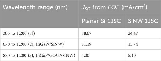
Table 2. Planar Si and SiNW 1JSC JSC derived from 1 sun EQE measurements at various wavelength ranges.
3.1.3 Laser beam-induced current mapping
To observe the current uniformity of planar Si and SiNW solar cells, LBIC measurements were acquired after ITO layer sputtering. Figures 7A, B show the LBIC maps of planar Si and SiNW solar cells, respectively. Their average LBIC and normalized current uniformities calculated using Equation 3 are listed in Table 3. The low-current regions are the busbar and the grid fingers of the solar cells, while the high-current regions are the active cell areas. Comparing the active regions of the cells, SiNW was found to yield larger current production than the planar Si. This agrees with the JSC of the SiNW solar cell acquired from J–V characteristics and EQE measurements, being larger than those of the planar Si solar cell. Although the maps were acquired at zero-bias (V = 0) conditions, it should be noted that the LBIC is much less than the JSC because the LBIC is the current measured per laser spot area and only uses a single-wavelength light source. SiNW LBIC yielded lower
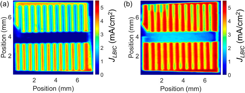
Figure 7. LBIC maps measured from (A) planar Si and (B) SiNW 1JSCs at room temperature and zero-bias (V = 0 V) conditions.

Table 3. Average LBIC, JLBIC,ave, and normalized current uniformities,
3.2 Planar Si and SiNW solar cells at various concentration factors and operating temperatures
After 1JSC measurements at 1 sun, room temperature, pulsed J–V characteristics, EQE and LBIC measurements were done at various temperatures. To allow fair comparison and to be accommodated by the contact probes of the pulsed J–V characteristic measurement setup, each of the best-performing planar Si and SiNW solar cells was mounted on a Cu plate.
3.2.1 Pulsed J–V characteristic measurements
Pulsed J–V characteristic curves of Cu-plate-mounted planar Si and SiNW solar cells are shown in Supplementary Figure S2. These curves were obtained at various concentration factors and cell temperatures. Although SiNW solar cell performance is superior at 1 sun, shunt resistances (RSH) became more severe with concentration factors of 15 suns and higher, compared to planar Si (Supplementary Tables S1, S2). These results suggest that the increased concentration factor aggravates surface recombination in SiNWs. To solve this, surface passivation or two-step H2 annealing (Jevasuwan et al., 2017) of SiNW solar cells is recommended. Moreover, although the RSH trend generally decreased with an increasing concentration factor, some data points deviated from this trend, particularly at 2.5 suns and 25°C and 40°C for planar 1JSC and at 7.5 suns and 25°C and 2.5 suns and 40°C for SiNW 1JSC, as shown in Supplementary Figures S3A, B. This is attributed to the flashing duration of the pulsed lamp used, which ranges between 50 µs and 2 m, as described in Section 2.3.1. This can cause some fluctuations during current measurement at each voltage applied because of the variability in the Xe lamp used (De Rooij, 2024; Chawla, 2024), which then affects the RSH calculation using Equation 1. On the other hand, it is difficult to comment on the evolution of series resistance (RS) with temperature since these values are within the same order of magnitude (Supplementary Tables S3, S4; Supplementary Figures S3C, D). Nevertheless, the calculated RS for both samples at any temperature decreased with increasing concentration factor. Because the flash lamp irradiated the whole area of the cell, the RS trend with increasing concentration factor may be attributed to the photon healing effect occurring within the cell perimeter, thereby increasing lateral transport efficiency (Ramspeck et al., 2007; Trupke et al., 2007; Hinken et al., 2007; Kampwerth et al., 2008; Xu et al., 2019). However, the photon healing effect was found insufficient to reduce surface recombination, most especially with SiNW solar cells characterized at higher concentration factors.
Figures 8A, B and Supplementary Tables S5, S6 show the evolution of JSC with an increasing concentration factor at various operating temperatures of planar Si and SiNW solar cells, respectively. Here, the error bars indicate the standard deviation of three measurement trials. The SiNW solar cell yielded a larger JSC than the planar Si. Based on the shape of the J–V curves, the larger JSC in SiNW solar cells is partially due to the leakage current brought about by surface defects and, hence, not necessarily a desirable current increase. This agrees with the lower RSH values calculated at higher concentration factors, as discussed earlier. The trend of planar Si and SiNW solar cells’ VOC with increasing cell temperature and concentration factor showed no difference, as plotted in Figures 8C, D and listed in Supplementary Tables S7, S8. On the other hand, the planar Si 1JSC VOC values were found to be generally larger than those of the SiNW 1JSC, which is contrary to the observation made before they were mounted on a Cu plate, as shown in Figure 5 and Table 1. This contrasting observation then suggests that the contact quality of the back electrode of the planar Si 1JSC with the In paste and the Cu plate is better than that of the SiNW 1JSC.
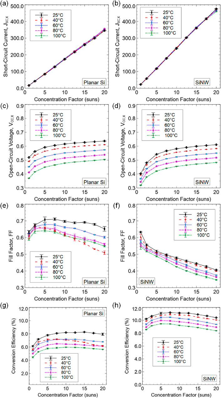
Figure 8. (A–B) JSC, (C–D) VOC, (E–F) FF, and (G–H) η of the best performing planar Si and SiNW 1JSCs mounted on the Cu plate, respectively, at various cell operating temperatures and concentration factors. The error bars indicate the standard deviation derived from three trials of measurements. The JSC, VOC, and FF values plotted in (A–F) were directly obtained from raw J–V characteristics shown in Supplementary Figure S2, while the η values plotted in (G, H) were adjusted by +0.77% and +4.53% to eliminate the parasitic resistance effects caused by Cu plate mounting using the In paste. The calculation of η value adjustments, Δη, is discussed in Supplementary Material, Section 1.2.
Figure 8E and Supplementary Table S9 show that an optimal FF is achieved at approximately 5 suns for the planar Si solar cell. On the other hand, the FF of the SiNW solar cell degraded with an increased concentration factor at any cell operating temperature (Figure 8F; Supplementary Table S10). Moreover, the decrease in FF of the SiNW solar cell with increasing cell temperature is sharper as compared to the FF of the planar Si solar cells. Aside from having a lower-quality Cu plate contact, these observed degradations can be explained as follows. As temperature increases, the rate of electron–hole recombination increases. This phenomenon is particularly pronounced in SiNW structures due to their high surface-to-volume ratio, which leads to more surface states that can act as recombination centers. In addition, as light concentration increases, the number of charge carriers generated in the SiNW solar cell also increases significantly. This leads to higher recombination rates, especially in the presence of defects or impurities in the SiNW. The increased recombination reduces the effective RSH, which then degrades the FF as more carriers are lost before contributing to the output current. These findings further confirm the detrimental effect of surface defects in the SiNW solar cell with increasing concentration factor. Consequently, the conversion efficiency, η, of the planar Si 1JSC (Figure 8G; Supplementary Table S11) at a higher concentration factor is generally superior to that of the SiNW 1JSC (Figure 8H; Supplementary Table S12).
The η values in Figures 8G, H were adjusted by +0.77% and +4.53% to eliminate the parasitic resistance effects caused by Cu plate mounting using the In paste. The calculation of η value adjustments, Δη, can be found in Supplementary Material, Section 1.2. The optimal concentration factor that yields the highest conversion efficiencies for solar cells is approximately 7.5 suns at cell temperatures of 40°C. In particular, the absolute conversion efficiency under these conditions is 1.05% higher than that under 1 sun. Upon comparing to a planar Si 1JSC under the same condition, the SiNW 1JSC achieved a 3.75% absolute increase in conversion efficiency. In CPV systems, there exists an optimal concentration factor at which a solar cell operates most efficiently. If the concentration factor exceeds this optimal level, thermodynamic principles indicate that a portion of the concentrated sunlight will be lost as heat, leading to reduced efficiency. Therefore, SiNW solar cells would be more suitable for low-concentration photovoltaic applications rather than for high-concentration scenarios.
3.2.2 One-sun EQE measurements at different cell operating temperatures
The EQE responses of Cu plate-mounted planar Si and SiNW solar cells are shown in Figures 9A, B, respectively. The redshift of EQE tails with increasing cell operating temperatures indicates bandgap reduction and is a typical behavior for a semiconductor device (Varshni, 1967; Tobnaghi et al., 2013; Schlangenotto et al., 1974; Lautenschlager et al., 1985; Alex et al., 1996; Loureno et al., 2004; Ishitani et al., 1994). As one may infer from the JSC values derived from EQE measurements using Equation 2 (Table 4), this redshift can be beneficial if the SiNW is used as a lower bandgap subcell in an MJSC structure. This can be inferred from the higher JSC calculated at higher temperatures for the 870–1,200 nm range.
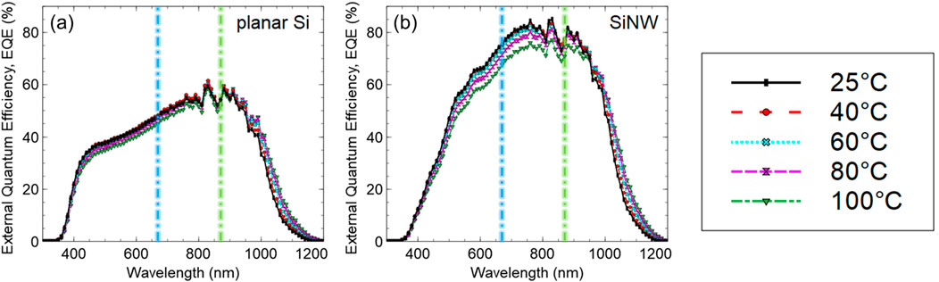
Figure 9. One-sun EQE response of Cu-mounted (A) planar Si and (B) SiNW solar cells at various cell operating temperatures.
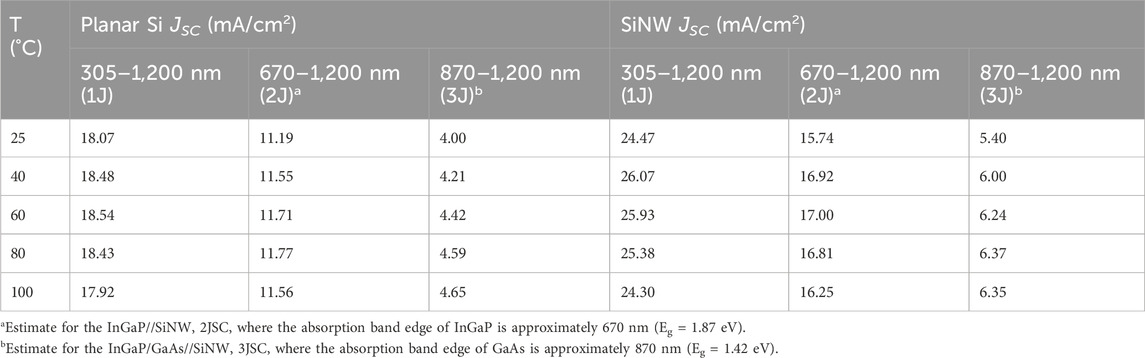
Table 4. Planar Si and SiNW solar cell JSC calculated from 1 sun EQE measurements at various wavelength ranges and operating temperatures.
On the other hand, the reduction in the EQE response with increasing cell temperature is more abrupt in the SiNW than that of the planar Si, particularly at wavelengths between 450 nm and 950 nm. This suggests that more events of carrier recombination could happen in the SiNW at high operating temperatures, which can happen at higher concentration factors due to thermal runaway. This agrees with the sharp decrease in FF with increasing concentration factor and cell operating temperature, as discussed in Section 3.2.1. Therefore, when using the SiNW solar cell for CPV applications, a cooling system should be included in the system design to help maintain lower operating temperatures. In addition, we can increase the p-shell growth time during CVD (Adachi et al., 2013) to possibly achieve EQE tail redshift in the SiNW, which will be favorable to the current-matching within III–V on SiNW MJSCs. However, if the p-shell is too thick, the SiNW 1JSC may experience increased recombination due to defect formation (Adachi et al., 2013), doping imbalances, and increased resistance (Kendrick et al., 2017). Therefore, the p-shell must be optimized to achieve EQE tail redshift without compromising on the SiNW 1JSC device quality.
3.2.3 LBIC mapping at various cell temperatures
Figure 10A–E and Figure 10F–J show the LBIC maps of Cu plate-mounted planar Si and SiNW 1JSCs, respectively, at cell temperatures between 25°C and 100°C, and Table 5 provides a summary of their averaged LBIC, JLBIC,ave, and normalized current uniformity, σJ/JLBIC,ave. The JLBIC,ave of the SiNW 1JSC was consistently higher than that of the planar Si at any cell temperature. However, as discussed earlier, a portion of the SiNW current may increase due to shunt leakage, which is not necessarily desirable. Meanwhile, current degradation with increasing cell temperature was observed in both solar cells. This observed decrease in current is attributed to an increase in nonradiative recombination events at higher temperatures brought about by elevated energy of charge carriers in the device (Schubert et al., 2018; Shaker et al., 2024). On the other hand, σJ/JLBIC,ave has no definite trend in both cells. As it does not vary by more than hundredths, it may be inferred that the σJ/JLBIC,ave did not vary with cell temperature, as previously observed in III–V solar cell materials (Yu Jeco et al., 2019a; Yu Jeco et al., 2018a).
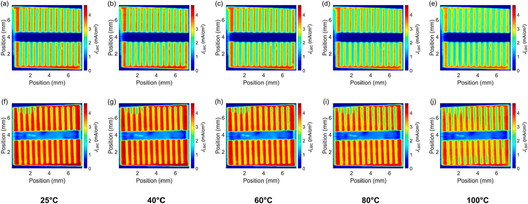
Figure 10. LBIC measurements acquired from Cu-mounted (A–E) planar Si and (F–J) SiNW solar cell at cell operating temperatures between 25°C and 100°C.
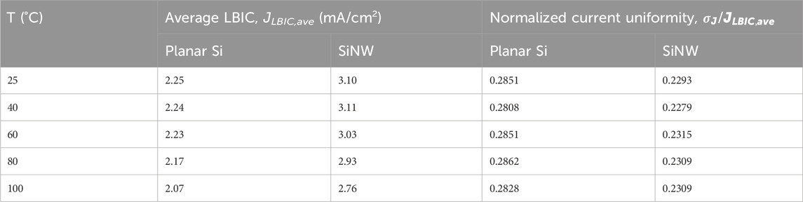
Table 5. Average LBIC current, JLBIC,ave, and normalized current uniformity, σJ/JLBIC,ave, of Cu-mounted planar Si and SiNW 1JSCs at different cell temperatures.
3.3 Characterizing the SiNW as a bottom cell for III–V MJSC
As mentioned earlier, SiNWs are attractive candidates as the bottom cell material for III–V-based MJSCs because they have better light trapping and a shorter charge separation distance in the junction than their planar counterparts. In this section, we characterized the EQE of SiNW 1JSC with and without the InGaP/GaAs 2J filter, and each active layer of the InGaP/GaAs 2JSC was measured. As shown in Figure 11, adding an SiNW as a bottom cell to the III–V 2JSC extended the absorption range to the infrared region, from approximately 850 nm to 1,200 nm. In Figure 11, the EQE of planar 1JSC was added for ease of comparison. Comparing the SiNW EQE as 1JSC under the InGaP/GaAs 2J filter, it can be observed that the filtered SiNW has a lower EQE than the unfiltered SiNW 1JSC at 850 nm–1,200 nm. This could be due to optical losses, such as reflection and destructive light interference, in the 2J filter.
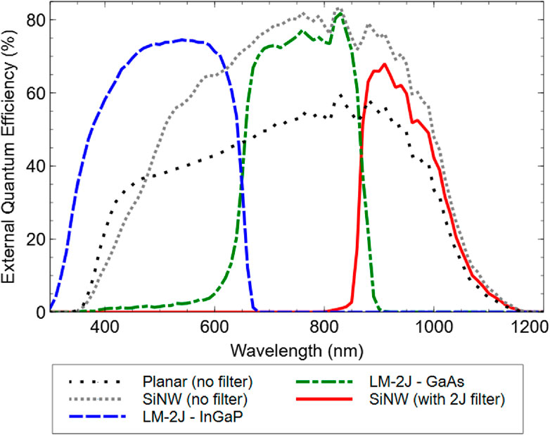
Figure 11. Measured EQE of planar and SiNW 1JSC without the 2J filter (dotted lines), SiNW 1JSC with the 2J filter (solid line), InGaP/GaAs 2JSC (dashed line), and InGaP/GaAs 2JSC in series with the SiNW 1JSC (dash–dotted line).
Based on the derived ISC from independent EQE measurements of InGaP/GaAs 2JSC and SiNW 1JSC with and without the 2J filter (Table 6), the latter will be limiting the current of the InGaP/GaAs//SiNW 3JSC. This is also considering that the InGaP/GaAs 2JSC, measured independently, has an active area, Acell, of 1.00 cm2 and that it is made up of direct bandgap III–V absorbers, which can deliver much higher power conversion efficiency than Si. Thus, for the 1-sun J–V characteristic measurement, we applied a laser-cut metal mask with a 0.20 cm2 aperture on top of the 1.00-cm2 InGaP/GaAs 2JSC to reduce the current production on it. The resultant J–V curves and the derived electrical performances are shown in Figure 12 and Table 7, respectively. With a 0.20-cm2 mask, the InGaP/GaAs 2JSC became the current-limiting cell. This suggests that there is an optimal active area that will current-match the SiNW bottom cell. This observation implicitly agrees with that of a recent theoretical study (Yu Jeco-Espaldon and Okada, 2023), in which a GaAs/Si tandem absorber was conjectured to deliver the optimal efficiency if the Si bottom cell area is 1.5 times larger than the upper III–V cell area. Thus, for a 0.39-cm2 SiNW 1JSC with the ITO conductive layer, the optimal active area of the upper InGaP/GaAs 2JSC could be approximately 0.26 cm2. This approach is also favorable to the device cost because the optimal area suggested reduces the amount of the III–V material needed.
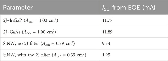
Table 6. JSC of the InGaP/GaAs 2JSC and SiNW 1JSC with and without the InGaP/GaAs 2J filter calculated from 1 sun EQE measurements at room temperature.
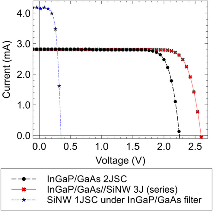
Figure 12. Measured AM 1.5G, 1-sun J–V characteristic curves of SiNW 1JSC, InGaP/GaAs 2JSC, and InGaP/GaAs 2JSC in series with the SiNW 1JSC. The measurements with the InGaP/GaAs 2JSC were obtained, while a laser-cut metal mask with a 0.20-cm2 square aperture was placed on top of the 2JSC in an attempt to match the current generation of the SiNW 1JSC.
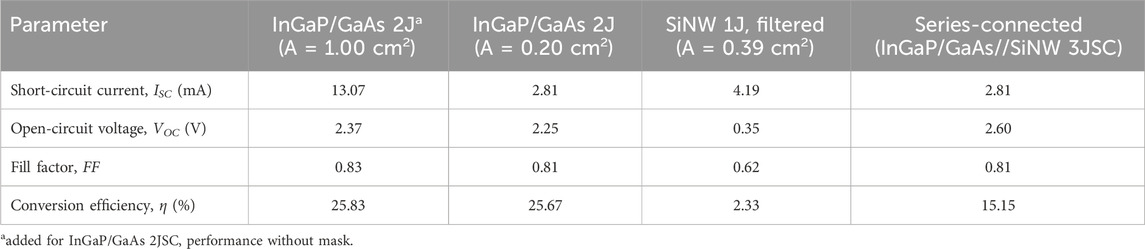
Table 7. Summary of electrical performance of the SiNW 1JSC, InGaP/GaAs 2JSC, and InGaP/GaAs 2JSC in series with the SiNW 1JSC under 1-sun, AM 1.5G, room temperature.
It can be noticed that there is a discrepancy between the ISC derived from the EQE and the one measured under 1-sun J–V characteristics. This can be attributed to differences in the light sources used in these independent measurements. The EQE measurement typically employs a monochromatic light source, whereas the 1-sun J–V characteristic measurement uses a solar simulator lamp, which aims to replicate the solar spectrum. Variations in the spectral output and intensity distribution between these light sources can lead to differences in the ISC values (Sheng et al., 2021; Park et al., 2023; National Renewable Energy Laboratory, 2024).
On a further note, the SiNW 1JSC characterized was fabricated without NW passivation and H2 annealing. To further boost the conversion efficiency of III–V//SiNW MJSCs, one may add surface passivation and H2 annealing steps (Jevasuwan et al., 2017; Yang and Zeng, 2021; Wang et al., 2014; Li et al., 2013). These are already known to reduce surface defects, which is one of the main challenges in fabricating a nanostructured solar cell. If we then improve the quality of SiNW bottom cells, we may be able to further reduce the active area of the upper III–V subcell for optimal current matching in a III–V//SiNW MJSC device.
Aside from III–V upper subcell area reduction, another approach that can be explored to achieve low payload, flexible, and high-efficiency III–V//SiNW MJSCs for electric vehicle applications is reducing their thickness. In particular, substrate removal by epitaxial lift-off (ELO) (Bauhuis et al., 2014; Konagai et al., 1978) and substrate thickness reduction by wet chemical etching (Duda et al., 2012), dry etching (Yoo, 2010), or a combined approach of continuous-plasma CVD and contact-free laser transfer printing technique (Li et al., 2024; Xiong et al., 2018; Sheng et al., 2014; Lumb et al., 2014) can be applied. In this work, no substrate thinning was done for the SiNW 1JSC. Thus, compared to its planar counterpart, the percent weight reduction of Si, %ΔwSi, is only 1.8% for an SiNW fabricated in a 280-µm-thick substrate. However, if we fabricate an SiNW 1JSC on a 100-µm-thick Si substrate, %ΔwSi of approximately 64.5% can be achieved. The detailed calculation can be found in Supplementary Material and Section 1.3.
4 Conclusion
This study demonstrated that nanoimprinted SiNW solar cells achieve optimal efficiency under low sunlight concentration at temperatures of 40°C or lower and a concentration factor of 7.5 suns, resulting in a 1.05% increase in conversion efficiency compared to unconcentrated light and a 3.75% increase over planar Si solar cells. The integration of SiNW 1JSC with a commercial InGaP/GaAs dual-junction solar cell shows promise for multijunction applications as a smaller active area in the III–V upper subcell enhances current matching, thereby potentially reducing costs. Additionally, while the SiNW solar cell exhibits a weight reduction of 1.8% compared to its planar counterpart, strategies to further improve this reduction to 64.5% and beyond can be achieved through SiNW solar cell substrate thinning, highlighting the potential of SiNW solar cells for flexible, lightweight, high-performance applications in electric vehicles and other terrestrial applications.
Data availability statement
The original contributions presented in the study are included in the article/Supplementary Material, further inquiries can be directed to the corresponding author.
Author contributions
BYJ-E: conceptualization, data curation, formal analysis, funding acquisition, investigation, methodology, software, validation, visualization, writing–original draft, and writing–review and editing. WJ: data curation, formal analysis, investigation, methodology, validation, and writing–review and editing. YO: conceptualization, formal analysis, funding acquisition, project administration, resources, supervision, validation, and writing–review and editing. NF: conceptualization, formal analysis, funding acquisition, project administration, resources, supervision, validation, and writing–review and editing.
Funding
The author(s) declare that financial support was received for the research, authorship, and/or publication of this article. This work was supported by the National Research and Development Agency, New Energy and Industrial Technology Development Organization (NEDO), the Ministry of Economy, Trade and Industry (METI), Japan, under Contract #2000942-0, the Japan Society for the Promotion of Science (Grant-in-Aid for Challenging Research—Exploratory 20K21135), and the Department of Science and Technology–Philippine Council for Industry, Energy & Emerging Technology (DOST-PCIEERD) Grant-in-Aid No. 1212673.
Acknowledgments
The authors would like to like thank Yumiko Sawabe, Mari Inoue, Susumu Soeya, and Yukinaga Arai (Namiki Foundry, National Institute for Materials Science) for the highly dedicated support they extended during the fabrication of SiNW solar cells. BYJ-E would like to thank the Department of Science and Technology-Balik Scientist Program (DOST-BSP) for receiving financial support. The Perplexity AI uses OpenAI’s ChatGPT 3.5 model.
Conflict of interest
The authors declare that the research was conducted in the absence of any commercial or financial relationships that could be construed as a potential conflict of interest.
Publisher’s note
All claims expressed in this article are solely those of the authors and do not necessarily represent those of their affiliated organizations, or those of the publisher, the editors and the reviewers. Any product that may be evaluated in this article, or claim that may be made by its manufacturer, is not guaranteed or endorsed by the publisher.
Supplementary material
The Supplementary Material for this article can be found online at: https://www.frontiersin.org/articles/10.3389/fnano.2024.1456915/full#supplementary-material
References
Adachi, M. M., Anantram, M. P., and Karim, K. S. (2013). Core-shell silicon nanowire solar cells. Sci. Rep. 3 (1), 1546. doi:10.1038/srep01546
Alanazi, F. (2023). Electric vehicles: benefits, challenges, and potential solutions for widespread adaptation. Appl. Sci. 13 (10), 6016. doi:10.3390/app13106016
Alex, V., Finkbeiner, S., and Weber, J. (1996). Temperature dependence of the indirect energy gap in crystalline silicon. J. Appl. Phys. 79 (9), 6943–6946. doi:10.1063/1.362447
Algora, C. (2007). Very-high-concentration challenges of III-V multijunction solar cells. Concentrator Photovoltaics (Springer Series in Optical Sciences Volume 130) 130, 89–111. doi:10.1007/978-3-540-68798-6
ASTM Standard Reference Spectra G173-03 (2012). Standard tables for reference solar spectral irradiances: direct normal and hemispherical on 37° tilted surface. West Conshohocken, Pennsylvania: ASTM International.
Azkar Ul, H. S., Aleem, Z. M., Park, S., and Junsin, Y. (2024). Stability challenges for a highly efficient perovskite/silicon tandem solar cell—a review. Sol. RRL 8 (2), 2300967. doi:10.1002/solr.202300967
Bajaj, J., Bubulac, L. O., Newman, P. R., Tennant, W. E., and Raccah, P. M. (1987). Spatial mapping of electrically active defects in HgCdTe using laser beam-induced current. J. Vac. Sci. Technol. A Vac. Surfaces Films 5 (5), 3186–3189. doi:10.1116/1.574834
Bauhuis, G. J., Mulder, P., and Schermer, J. J. (2014). Thin-film III–V solar cells using epitaxial lift-off. High-Efficiency Solar Cells: physics. Mater. Devices, 623–643. doi:10.1007/978-3-319-01988-8_21
Baur, C., Hermle, M., Dimroth, F., and Bett, A. W. (2007). Effects of optical coupling in III-V multilayer systems. Appl. Phys. Lett. 90 (19). doi:10.1063/1.2737927
Bett, A. J., and Yarema, M. (2022). Status and challenges of multi-junction solar cell technology. Front. Energy Res. 10, 971918. doi:10.3389/fenrg.2022.971918
Bunkokeiki (2012). Bunkokeiki Co. Ltd, BS-500BK Si photodiode detector. Available at: https://bunkoukeiki.co.jp/pdf/pdf/BS-500BK-1708023N-E.pdf.
Campbell, P., and Green, M. A. (1986). The limiting efficiency of silicon solar cells under concentrated sunlight. IEEE Trans. Electron Devices 33 (2), 234–239. doi:10.1109/T-ED.1986.22472
Chawla, M. K. (2024). A step by step guide to selecting a solar simulator. Version 3. Photoemission. Available at: https://photoemission.com/techpapers/A%20step%20by%20step%20guide%20to%20selecting%20a%20Solar%20Simulator%20Ver.%203.pdf (Accessed August 30, 2024).
Cotal, H., Fetzer, C., Boisvert, J., Kinsey, G., King, R., Hebert, P., et al. (2009). III–V multijunction solar cells for concentrating photovoltaics. Energy & Environ. Sci. 2 (2), 174–192. doi:10.1039/B809257E
Deng, X., Wen, X., Zheng, J., Young, T., Lau, J. C. F., Kim, J., et al. (2018). Dynamic study of the light soaking effect on perovskite solar cells by in-situ photoluminescence microscopy. J. Appl. Phys. 129 (24), 240901. doi:10.1063/1.5035464
Derkacs, D., Bilir, D. T., and Sabnis, V. A. (2012). Luminescent coupling in GaAs/GaInNAsSb multijunction solar cells. IEEE J. Photovoltaics 3 (1), 520–527. doi:10.1109/JPHOTOV.2012.2213579
De Rooij, D. (2024). Flash test: technical background and importance. Sinovoltaics. Available at: https://sinovoltaics.com/learning-center/testing/flash-test-technical-background-and-importance/(Accessed August 30, 2024).
Duda, A., Ward, S., and Young, M. (2012). Inverted metamorphic multijunction IMM cell processing instructions. Golden, CO United States: National Renewable Energy Lab.NREL.
Elrashidi, A. (2022). Light harvesting in silicon nanowires solar cells by using graphene layer and plasmonic nanoparticles. Appl. Sci. 12 (5), 2519. doi:10.3390/app12052519
Essig, S., Allebe, C., Remo, T., Geisz, J. F., Steiner, M. A., Horowitz, K., et al. (2017). Raising the one-sun conversion efficiency of III–V/Si solar cells to 32.8% for two junctions and 35.9% for three junctions. Nat. Energy 2 (9), 17144. doi:10.1038/nenergy.2017.144
Fitchette, M., and Freundlich, A. (2016). “Material considerations for terawatt level deployment of III-V multi-junction photovoltaics,” in 2016 IEEE 43rd Photovoltaic Specialists Conference (PVSC), Portland, OR, USA, 05–10 June, 2016.
Fraunhofer Institute for Solar Energy Systems(2022). Fraunhofer ISE develops the world’s most efficient solar cell with 47.6 percent efficiency.
Friedman, D. J., Geisz, J. F., and Steiner, M. A. (2013). Analysis of multijunction solar cell current–voltage characteristics in the presence of luminescent coupling. IEEE J. Photovoltaics 3 (4), 1429–1436. doi:10.1109/JPHOTOV.2013.2275189
Friedman, D. J., Geisz, J. F., and Steiner, M. A. (2014). Effect of luminescent coupling on the optimal design of multijunction solar cells. IEEE J. Photovoltaics 4 (3), 986–990. doi:10.1109/JPHOTOV.2014.2308722
Fukata, N., Subramani, T., Jevasuwan, W., Dutta, M., and Bando, Y. (2017). Functionalization of silicon nanostructures for energy-related applications. Small 13 (45), 1701713. doi:10.1002/smll.201701713
Garnett, E., and Yang, P. (2010). Light trapping in silicon nanowire solar cells. Nano Lett. 10 (3), 1082–1087. doi:10.1021/nl100161z
Green, M. A., Jianhua, Z., Blakers, A. W., Taouk, M., and Narayanan, S. (1986). 25-percent efficient low-resistivity silicon concentrator solar cells. IEEE Electron Device Lett. 7 (10), 583–585. doi:10.1109/EDL.1986.26481
Hinken, D., Ramspeck, K., Bothe, K., Fischer, B., and Brendel, R. (2007). Series resistance imaging of solar cells by voltage dependent electroluminescence. Appl. Phys. Lett. 91 (18). doi:10.1063/1.2804562
Hirst, L. C., and Ekins-Daukes, N. J. (2011). Fundamental losses in solar cells. Prog. Photovoltaics Res. Appl. 19 (3), 286–293. doi:10.1002/pip.1024
Honsberg, C., and Bowden, S. (2010). Chapter 8 – introduction. PVEducation.Org. Available at: https://www.pveducation.org/pvcdrom/characterisation/introduction (Accessed January 11, 2023).
Hou, Y., Aydin, E., De Bastiani, M., Xiao, C., Isikgor, F. H., Xue, D. J., et al. (2020). Efficient tandem solar cells with solution-processed perovskite on textured crystalline silicon. Science 367 (6480), 1135–1140. doi:10.1126/science.aaz3691
Huang, B. R., Yang, Y. K., Lin, T. C., and Yang, W. L. (2012). A simple and low-cost technique for silicon nanowire arrays based solar cells. Sol. Energy Mater. Sol. Cells 98, 357–362. doi:10.1016/j.solmat.2011.11.031
Ishitani, Y., Minagawa, S., and Tanaka, T. (1994). Temperature dependence of the band-gap energy of disordered GaInP. J. Appl. Phys. 75 (10), 5326–5331. doi:10.1063/1.355735
Jevasuwan, W., Nakajima, K., Sugimoto, Y., and Fukata, N. (2016). Metal-catalyzed electroless etching and nanoimprinting silicon nanowire-based solar cells: silicon nanowire defect reduction and efficiency enhancement by two-step H2 annealing. Jpn. J. Appl. Phys. 55 (6), 065001. doi:10.7567/JJAP.55.065001
Jevasuwan, W., Pradel, K. C., Subramani, T., Chen, J., Takei, T., Nakajima, K., et al. (2017). Diffused back surface field formation in combination with two-step H2 annealing for improvement of silicon nanowire-based solar cell efficiency. Jpn. J. Appl. Phys. 56 (4S), 04CP01. doi:10.7567/JJAP.56.04CP01
Jung, J. Y., Um, H. D., Jee, S. W., Park, K. T., Bang, J. H., and Lee, J. H. (2013). Optimal design for antireflective Si nanowire solar cells. Sol. Energy Mater. Sol. Cells 112, 84–90. doi:10.1016/j.solmat.2012.12.046
Kampwerth, H., Trupke, T., Weber, J. W., and Augarten, Y. (2008). Advanced luminescence based effective series resistance imaging of silicon solar cells. Appl. Phys. Lett. 93 (20). doi:10.1063/1.2982588
Kazuaki, S., and Takaaki, A. (2011). Multi-junction compound semiconductor solar cell, worldwide patent application, sharp KK. Available at: https://worldwide.espacenet.com/patent/search?q=pn%3DWO2011078378A1.
Kendrick, C., Kuo, M. W., Li, J., Shen, H., Mayer, T. S., and Redwing, J. M. (2017). Uniform p-type doping of silicon nanowires synthesized via vapor-liquid-solid growth with silicon tetrachloride. J. Appl. Phys. 122 (23). doi:10.1063/1.4993632
Kim, H. T., Lee, K., Jin, W., Um, H. D., Lee, M., Hwang, E., et al. (2018). Phosphorescent energy downshifting for diminishing surface recombination in silicon nanowire solar cells. Sci. Rep. 8 (1), 16974. doi:10.1038/s41598-018-35356-w
King, R. R., Bhusari, D., Boca, A., Larrabee, D., Liu, X. Q., Hong, W., et al. (2011). Band gap-voltage offset and energy production in next-generation multijunction solar cells. Prog. Photovoltaics Res. Appl. 19 (7), 797–812. doi:10.1002/pip.1044
Köhnen, E., Wagner, P., Lang, F., Cruz, A., Li, B., Roß, M., et al. (2021). 27.9% efficient monolithic perovskite/silicon tandem solar cells on industry compatible bottom cells. Sol. RRL 5 (1), 2100244. doi:10.1002/solr.202100244
Konagai, M., Sugimoto, M., and Takahashi, K. (1978). High efficiency GaAs thin film solar cells by peeled film technology. J. Cryst. growth 45, 277–280. doi:10.1016/0022-0248(78)90449-9
Kumar, D., Srivastava, S. K., Singh, P. K., Husain, M., and Kumar, V. (2011). Fabrication of silicon nanowire arrays based solar cell with improved performance. Sol. Energy Mater. Sol. Cells 95 (1), 215–218. doi:10.1016/j.solmat.2010.04.024
Lautenschlager, P., Allen, P. B., and Cardona, M. (1985). Temperature dependence of band gaps in Si and Ge. Phys. Rev. B 31 (4), 2163–2171. doi:10.1103/PhysRevB.31.2163
Lee, K. H., Barnham, K. W., Connolly, J. P., Browne, B. C., Airey, R. J., Roberts, J. S., et al. (2011). Demonstration of photon coupling in dual multiple-quantum-well solar cells. IEEE J. Photovoltaics 2 (1), 68–74. doi:10.1109/JPHOTOV.2011.2177444
Li, J., and Wang, (2004). Comparison between quantum confinement effects of quantum wires and dots. Chem. Mater. 16 (21), 4012–4015. doi:10.1021/cm0494958
Li, K., Wang, X., Lu, P., Ding, J., and Yuan, N. (2013). The influence of passivation and photovoltaic properties of α-Si: H coverage on silicon nanowire array solar cells. Nanoscale Res. Lett. 8, 396–410. doi:10.1186/1556-276x-8-396
Li, Y., Ru, X., Yang, M., Zheng, Y., Yin, S., Hong, C., et al. (2024). Flexible silicon solar cells with high power-to-weight ratios. Nature 626 (7997), 105–110. doi:10.1038/s41586-023-06948-y
Liu, J., He, Y., Ding, L., He, B., and Xu, X. (2023) “34% efficient perovskite/silicon tandem using CZ-based silicon solar cell,” in Presented at the 34th International Photovoltic Science and Technology Conference, Shenzhen, China.
Loureno, S. A., Dias, I. F., Duarte, J. L., Laureto, E., Poças, L. C., Toginho Filho, D. O., et al. (2004). Thermal expansion contribution to the temperature dependence of excitonic transitions in GaAs and AlGaAs. Braz. J. Phys. 34, 517–525. doi:10.1590/S0103-97332004000300031
Lueck, M. R., Andre, C. L., Pitera, A. J., Lee, M. L., Fitzgerald, E. A., and Ringel, S. A. (2006). Dual junction GaInP/GaAs solar cells grown on metamorphic SiGe/Si substrates with high open circuit voltage. IEEE Electron Device Lett. 27 (3), 142–144. doi:10.1109/LED.2006.870250
Lumb, M. P., Meitl, M., Wilson, J., Bonafede, S., Burroughs, S., Forbes, D. V., et al. (2014). “Development of InGaAs solar cells for> 44% efficient transfer-printed multi-junctions,” in In2014 IEEE 40th Photovoltaic Specialist Conference (PVSC), Denver, CO, USA, 08–13 June, 2014, 0491–0494. doi:10.1109/pvsc.2014.69249671
Mi, Z., and Chang, Y. L. (2009). III-V compound semiconductor nanostructures on silicon: epitaxial growth, properties, and applications in light emitting diodes and lasers. J. Nanophot. 3 (1), 031602. doi:10.1117/1.3081051
Nakamura, T., Imaizumi, M., Murai, K., Kawamura, R., and Nanno, I. (2023). Mechanism of thermal runaway in solar cells. Jpn. J. Appl. Phys 62 (SK), p.SK1049. doi:10.35848/1347-4065/accfa4
National Renewable Energy Laboratory (2024). Spectral mismatch corrections video text version. Available at: https://www.nrel.gov/news/video/text-spectral-mismatch-corrections.html (Accessed August 28, 2024).
Oh, J., Yuan, H. C., and Branz, H. M. (2012). An 18.2%-efficient black-silicon solar cell achieved through control of carrier recombination in nanostructures. Nat. Nanotechnol. 7 (11), 743–748. doi:10.1038/nnano.2012.166
Park, J. H., Hwang, S. K., Ji, S. G., and Kim, J. Y. (2023). Characterization of various tandem solar cells: protocols, issues, and precautions. InExploration 3 (2), 20220029. doi:10.1002/exp.20220029
Ramspeck, K., Bothe, K., Hinken, D., Fischer, B., Schmidt, J., and Brendel, R. (2007). Recombination current and series resistance imaging of solar cells by combined luminescence and lock-in thermography. Appl. Phys. Lett. 90 (15). doi:10.1063/1.2721138
Rühle, S. (2016). Tabulated values of the Shockley–Queisser limit for single junction solar cells. Sol. energy 130, 139–147. doi:10.1016/j.solener.2016.02.015
Schlangenotto, H., Maeder, H., and Gerlach, W. (1974). Temperature dependence of the radiative recombination coefficient in silicon. Phys. status solidi (a) 21 (1), 357–367. doi:10.1002/pssa.2210210140
Schnabel, M., Schulte-Huxel, H., Rienäcker, M., Warren, E. L., Ndione, P. F., Nemeth, B., et al. (2020). Three-terminal III–V/Si tandem solar cells enabled by a transparent conductive adhesive. Sustain. Energy & Fuels 4 (2), 549–558. doi:10.1039/c9se00893d
Schubert, E. F. (2018). “Theory of radiative recombination,” in Light-emitting diodes. 3rd ed. New York: Cambridge University Press.
Schulze, P. S. C., Bett, A. J., Bivour, M., Caprioglio, P., Gerspacher, F. M., Kabaklı, Ş. Ö., et al. (2020). 25.1% high-efficiency monolithic perovskite silicon tandem solar cell with a high bandgap perovskite absorber. Sol. RRL 4 (2), 2000152. doi:10.1002/solr.202000152
Schygulla, P., Muller, R., Hohn, O., Schochtner, M., Chojniak, D., Cordaro, A., et al. (2023) “Wafer bonded two-terminal III-V//Si triple-junction solar cell with power conversion efficiency of 36.1% at AM1.5G,” in Presented at the 40th European Photiovoltaic Solar Energy Conference, Lisbon, Portugal.
Schygulla, P., Müller, R., Lackner, D., Höhn, O., Hauser, H., Bläsi, B., et al. (2022). Two-terminal III–V//Si triplejunction solar cell with power conversion efficiency of 35.9% at AM1.5g. Prog. Photovolt. 30 (8), 869–879. doi:10.1002/pip3503
Shaker, L. M., Al-Amiery, A. A., Hanoon, M. M., Al-Azzawi, W. K., and Kadhum, A. A. (2024). Examining the influence of thermal effects on solar cells: a comprehensive review. Sustain. Energy Res. 11 (1), 6. doi:10.1186/s40807-024-00100-8
Sheng, G., Xiaodong, L., and Shuxian, L. (2021). Spectral mismatch and its effect on artificial solar light source under standard test conditions. E3S Web Conf. 292, 01021. doi:10.1051/e3sconf/202129201021
Sheng, X., Bower, C. A., Bonafede, S., Wilson, J. W., Fisher, B., Meitl, M., et al. (2014). Printing-based assembly of quadruple-junction four-terminal microscale solar cells and their use in high-efficiency modules. Nat. Mater. 13 (6), 593–598. doi:10.1038/nmat3946
Sinton, R. A., Kwark, Y., Gan, J. Y., and Swanson, R. M. (1986). 27.5-percent silicon concentrator solar cells. IEEE Electron Device Lett. 7 (10), 567–569. doi:10.1109/EDL.1986.26476
Sinton, R. A., and Swanson, R. M. (1987). Design criteria for Si point-contact concentrator solar cells. IEEE Trans. Electron Devices 34 (10), 2116–2123. doi:10.1109/T-ED.1987.23205
Slade, A., and Garboushian, V. (2005). “27.6% efficient silicon concentrator solar cells for mass production,” in Technical Digest, 15th International Photovoltaic Science and Engineering Conference, Beijing.
Stauch, A. (2021). Does solar power add value to electric vehicles? An investigation of car-buyers’ willingness to buy product-bundles in Germany. Energy Res. & Soc. Sci. 75, 102006. doi:10.1016/j.erss.2021.102006
Steiner, M. A., Geisz, J. F., Moriarty, T. E., France, R. M., McMahon, W. E., Olson, J. M., et al. (2012). Measuring IV curves and subcell photocurrents in the presence of luminescent coupling. IEEE J. Photovoltaics 3 (2), 879–887. doi:10.1109/JPHOTOV.2012.2228298
Stelzner, T., Pietsch, M., Andrä, G., Falk, F., Ose, E., and Christiansen, S. (2008). Silicon nanowire-based solar cells. Nanotechnology 19 (29), 295203. doi:10.1088/0957-4484/19/29/295203
Takamoto, T., Kaneiwa, M., Imaizumi, M., and Yamaguchi, M. (2005). InGaP/GaAs-based multijunction solar cells. Prog. Photovoltaics Res. Appl. 13 (6), 495–511. doi:10.1002/pip.642
Tobnaghi, D. M., Madatov, R., and Naderi, D. (2013). The effect of temperature on electrical parameters of solar cells. Int. J. Adv. Res. Electr. Electron. Instrum. Eng. 2 (12), 6404–6407. Available at: https://www.ijareeie.com/upload/2013/december/2F_The%20Effect.pdf
Tong, C. (2023) “III-V-on-Si nanowire-based solar cells for tandem applications,” in Micro and nanotechnologies/Microelectronics. Université Paris-Saclay.
Trupke, T., Pink, E., Bardos, R. A., and Abbott, M. D. (2007). Spatially resolved series resistance of silicon solar cells obtained from luminescence imaging. Appl. Phys. Lett. 90 (9). doi:10.1063/1.2709630
Tsakalakos, L., Balch, J., Fronheiser, J., Korevaar, B. A., Sulima, O., and Rand, J. (2007). Silicon nanowire solar cells. Appl. Phys. Lett. 91 (23), 91. doi:10.1063/1.2821113
Varshni, Y. P. (1967). Temperature dependence of the energy gap in semiconductors. physica 34 (1), 149–154. doi:10.1016/0031-8914(67)90062-6
Vossier, A., Hirsch, B., and Gordon, J. M. (2010). Is Auger recombination the ultimate performance limiter in concentrator solar cells? Appl. Phys. Lett. 97 (19). doi:10.1063/1.3510474
Wang, F., Zhang, X., Wang, L., Jiang, Y., Wei, C., Sun, J., et al. (2014). Role of hydrogen plasma pretreatment in improving passivation of the silicon surface for solar cells applications. ACS Appl. Mater. & interfaces 6 (17), 15098–15104. doi:10.1021/am5031837
Xia, J. B., and Cheah, K. W. (1997). Quantum confinement effect in thin quantum wires. Phys. Rev. B 55 (23), 15688–15693. doi:10.1103/PhysRevB.55.15688
Xing, Y., Han, P., Wang, S., Liang, P., Lou, S., Zhang, Y., et al. (2015). A review of concentrator silicon solar cells. Renew. Sustain. Energy Rev. 51, 1697–1708. doi:10.1016/j.rser.2015.07.035
Xiong, K., Mi, H., Chang, T. H., Liu, D., Xia, Z., Wu, M. Y., et al. (2018). AlGaAs/Si dual-junction tandem solar cells by epitaxial lift-off and print-transfer-assisted direct bonding. Energy Sci. & Eng. 6 (1), 47–55. doi:10.1002/ese3.182
Xu, H., Delamarre, A., Yu Jeco, B. M., Johnson, H., Watanabe, K., Okada, Y., et al. (2019). Current transport efficiency analysis of multijunction solar cells by luminescence imaging. Prog. Photovoltaics Res. Appl. 27 (10), 835–843. doi:10.1002/pip.3140
Yamaguchi, M., Masuda, T., Araki, K., Sato, D., Lee, K. H., Kojima, N., et al. (2021). Development of high-efficiency and low-cost solar cells for PV-powered vehicles application. Prog. Photovoltaics Res. Appl. 29 (7), 684–693. doi:10.1002/pip.3343
Yamaguchi, M., Takamoto, T., Juso, H., Nakamura, K., Ozaki, R., Masuda, T., et al. (2024). Approaches for III-V/Si tandem solar cells and comparative studies on Si tandem solar cells. Prog. Photovolt. Res. Appl. 1–10. doi:10.1002/pip.3780
Yang, P., and Zeng, X. (2021). Effect of hydrogenated silicon film microstructure on the surface states of n-type silicon nanowires and solar cells. J. Mater. Sci. Mater. Electron. 32 (3), 3066–3071. doi:10.1007/s10854-020-05056-1
Yoo, J. (2010). Reactive ion etching (RIE) technique for application in crystalline silicon solar cells. Sol. Energy 84 (4), 730–734. doi:10.1016/j.solener.2010.01.031
Yoshikawa, K., Kawasaki, H., Yoshida, W., Irie, T., Konishi, K., Nakano, K., et al. (2017). Silicon heterojunction solar cell with interdigitated back contacts for a photoconversion efficiency over 26. Nat. energy 2 (5), 1–8. doi:10.1038/nenergy.2017.32
Yu, P., Wu, J., Liu, S., Xiong, J., Jagadish, C., and Wang, Z. M. (2016). Design and fabrication of silicon nanowires towards efficient solar cells. Nano Today 11 (6), 704–737. doi:10.1016/j.nantod.2016.10.001
Yu Jeco, B. M. F., Yoshida, K., Tamaki, R., Ahsan, N., and Okada, Y. (2017b). “Analysis of current generation in InGaP/GaAs/Ge triple junction solar cells with optically non-uniform luminescence coupling effect,” in Proc. 33rd Eur. Photovoltaic Sol. Energy Conf., 1236.
Yu Jeco, B. M., Sogabe, T., Ahsan, N., and Okada, Y. (2018a). Temperature dependence of luminescence coupling effect in InGaP/GaAs/Ge triple junction solar cells. J. Photonics Energy 8 (2), 1. doi:10.1117/1.JPE.8.022602
Yu Jeco, B. M., Sogabe, T., Ogura, A., Miyashita, N., Tamaki, R., and Okada, Y. (2016) “Laser beam induced current (LBIC) mapping of InGaP/GaAs/Ge triple junction solar cells with luminescence coupling,” in In2016 IEEE 43rd Photovoltaic Specialists Conference (PVSC), Portland, OR, USA, 05–10 June, 2016.
Yu Jeco, B. M., Sogabe, T., Tamaki, R., Ahsan, N., and Okada, Y. (2017a). Impact of optically nonuniform luminescence coupling effect to the limiting cell conversion efficiency in InGaP/GaAs/Ge triple junction solar cell. J. Photonics Energy 7 (3), 035501. doi:10.1117/1.JPE.7.035501
Yu Jeco, B. M., Tamaki, R., Nakamura, T., Imaizumi, M., Ahsan, N., and Okada, Y. (2018b) “Spatial evaluation of luminescent coupling effect in a current-limiting subcell of in GaP/GaAs/Ge triple junction solar cells,” in In2018 IEEE 7th World Conference on Photovoltaic Energy Conversion (WCPEC) (A Joint Conference of 45th IEEE PVSC, 28th PVSEC & 34th EU PVSEC), Waikoloa, HI, USA, 10–15 June 2018.
Yu Jeco, B. M., Veinberg-Vidal, E., Vauche, L., Ahsan, N., and Okada, Y. (2019a). Temperature dependence of wafer-bonded III-V on silicon multijunction solar cells with luminescent coupling effect. J. Photonics Energy 9 (1), 1. doi:10.1117/1.JPE.9.015503
Yu Jeco, B. M., Veinberg-Vidal, E., Vauche, L., Yoshida, K., Tamaki, R., Ahsan, N., et al. (2019b). Luminescent coupling effect in wafer-bonded III-V on silicon multijunction solar cells. J. Photonics Energy 9 (1), 1. doi:10.1117/1.JPE.9.015504
Yu Jeco-Espaldon, B. M., and Okada, Y. (2023). “Analysis of plateau tandem solar cells,” in 2023 IEEE International Future Energy Electronics Conference (IFEEC), Sydney, Australia, 20–23 November, 2023, 1–5. doi:10.1109/ifeec58486.2023.10458532
Yu Jeco-Espaldon, B. M., Wang, H., Espaldon, A. E., Kubo, T., Segawa, H., Ahsan, N., et al. (2020). Application of perovskite quantum dots in carrier redistribution in III-V multijunction solar cells with luminescent coupling effect. J. Photonics Energy 10 (4), 042005. doi:10.1117/1.JPE.10.042005
Zhao, Z., Yadavalli, K., Hao, Z., and Wang, K. L. (2008). Direct integration of III–V compound semiconductor nanostructures on silicon by selective epitaxy. Nanotechnology 20 (3), 035304. doi:10.1088/0957-4484/20/3/035304
Keywords: laser beam-induced current, multijunction solar cell, nanofabrication, solar cell characterization, silicon nanowire, III–V /silicon solar cells
Citation: Yu Jeco-Espaldon BM, Jevasuwan W, Okada Y and Fukata N (2024) Optimal performance of silicon nanowire solar cells under low sunlight concentration and their integration as bottom cells in III–V multijunction systems. Front. Nanotechnol. 6:1456915. doi: 10.3389/fnano.2024.1456915
Received: 29 June 2024; Accepted: 18 September 2024;
Published: 02 October 2024.
Edited by:
Keyla M. Fuentes, Spora Biotech, ChileReviewed by:
Sahil Tahiliani, Applied Materials, United StatesSandip Das, Kennesaw State University, United States
Mihir Kumar Sahoo, Indian Institute of Technology Bombay, India
Copyright © 2024 Yu Jeco-Espaldon, Jevasuwan, Okada and Fukata. This is an open-access article distributed under the terms of the Creative Commons Attribution License (CC BY). The use, distribution or reproduction in other forums is permitted, provided the original author(s) and the copyright owner(s) are credited and that the original publication in this journal is cited, in accordance with accepted academic practice. No use, distribution or reproduction is permitted which does not comply with these terms.
*Correspondence: Bernice Mae Yu Jeco-Espaldon, Ym15dWplY29AdXNhLmVkdS5waA==