 Sayani Majumdar
- Faculty of Information Technology and Communication Sciences, Tampere University, Tampere, Finland
The future computing beyond von Neumann era relies heavily on emerging devices that can extensively harness material and device physics to bring novel functionalities and can perform power-efficient and real time computing for artificial intelligence (AI) tasks. Additionally, brain-like computing demands large scale integration of synapses and neurons in practical circuits that requires the nanotechnology to support this hardware development, and all these should come at an affordable process complexity and cost to bring the solutions close to market rather soon. For bringing AI closer to quantum computing and space technologies, additional requirements are operation at cryogenic temperatures and radiation hardening. Considering all these requirements, nanoelectronic devices utilizing ferroic ordering has emerged as one promising alternative. The current review discusses the basic architectures of spintronic and ferroelectric devices for their integration in neuromorphic and analog memory applications, ferromagnetic and ferroelectric domain structures and control of their dynamics for reliable multibit memory operation, synaptic and neuronal leaky-integrate-and-fire (LIF) functions, concluding with their large-scale integration possibilities, challenges and future research directions.
Introduction
The future of computing beyond Complementary Metal Oxide Semiconductor (CMOS) era requires extensive use of material and device physics to perform computation at the atomic level (Manipatruni, 2018; Chen, 2022). Development of neuromorphic computing hardware, that is devices with bio-plausible functionalities for implementing neural network operations in hardware, requires different kinds of volatile and non-volatile memories to implement synaptic and neuronal functionalities. While synaptic plasticity, runtime weight update and supervised learning require well-controlled, multilevel conductance in nanoscale devices with long and short-term synaptic potentiation and depression, neuronal leaky-integrate-and-fire (LIF) activity demands accumulative nature of switching from one conductance state to the other and a finite decay rate of conductance states to return to its previous condition rather quickly.
For achieving multilevel conductance states, different physical phenomenon has been actively investigated by the scientists. This includes resistive random-access memories (RRAMs), phase-change memories (PCMs), conduction bridge memories (CBRAMs), magnetic random-access memories (MRAMs), ferroelectric random-access memories (FeRAMs) and so on (Xia, 2019; Ielmini, 2020; Majumdar, 2022b). Each technology provides some advantages and some challenges in terms of operational voltage requirement, speed, scalability, reliability, endurance, yield, manufacturability, cost etc. and no single technology has so far been able to provide solutions for all the requirements for high-performance memories and in-memory-computing (IMC). In the current review article, we will focus on the last two categories of emerging CMOS-compatible memories, i.e., MRAMs and FeRAMs as multilevel memories and their implementation in certain application areas that shows utilization of ferroic ordering can have significant advantage in non-volatile memory (NVM) and neuromorphic hardware development, operating down to deep cryogenic temperature.
Ferromagnetic (FM) and ferroelectric (FE) material based programmable memory devices can represent multiple conductance states due to their switchable polarization and internal domain structures that can be programmed controllably utilizing magnetic or electric field. These switched polarization states can retain their polarization after the applied field is withdrawn, and thus they can work as multi-level memory and synaptic devices for implementing neuromorphic functionalities. The multi-domain switching dynamics of FM or FE thin films are fundamentally different from most other memristive devices that involves electroforming processes and significant ion motion (in case of RRAMs or CBRAMs) or switching between crystalline and amorphous phases (like PCMs). Analog resistive states in FM or FE thin film devices are due to the non-coherent switching of the polarized domains, with polarization up and down states representing device On and Off states and mixed polarization phases leading to intermediate conductance states. Based on device architectures and operating principles, large conductance range, fast switching, programmable retention and power efficiency can be achieved in Ferroic devices. In particular, devices with ferromagnetic ordering can provide excellent endurance and more energy-efficient writing, due to the spin-based nature of magnetization switching with no charge movements in MRAMs (Grollier, 2020) while ferroelectric field-effect transistor (FeFET) technology offer large dynamic conductance range, analog operation and excellent CMOS compatibility (Jerry, 2017; Mulaosmanovic, 2017; Khan, 2020).
Traditionally, spintronic MRAMs and FeRAMs have been implemented as binary memory components. However, due to growing interest in neuromorphic device functionalities, it is of high relevance to investigate their multi-domain switching properties for replicating synaptic plasticity and membrane potential modulation for neuronic functionalities. Interestingly, the multidomain switching mechanisms of ferroic materials has resemblance with biological neural systems, like accumulative and stochastic nature of switching, providing the very promising possibilities for incorporating both short- and long-term memory operations that can be utilized to develop bio-realistic hardware primitives.
In addition to the need for multibit storage and computing, memories operating at cryogenic temperatures are becoming critical components for high performance computing (HPC), quantum technologies, space and superconducting electronics. For HPC, one significant demand is memories with capacities for handling of larger and faster data systems for applications such as data analytics and machine learning. Computing at cryogenic temperature has the potential to provide these functionalities through improvements in cycling time, power consumption, and higher compute density.
For quantum computers, there are three major components, quantum bits or qubits, a control processor, and a memory block. In the present-day quantum computers, a conventional computer operating at room temperature is used as the control processor. Long cables connect the qubits to the control processor. Although working satisfactorily for a small number of qubits, scalability of this architecture to even a few hundreds of qubits would be a big challenge due to the requirement of a large number of cables to maintain a connection between the room-temperature control processor and the qubits at cryogenic temperature. One way of circumventing the scaling issue is to place the control processor at a temperature close to that of the qubits. However, when the control processor is at 4 K or below, types of memories that can be used in conjunction with quantum computers, also become limited. Interconnects between the room-temperature memories and the cryogenic control processor would cause a significant thermal leakage and could generate thermal noise that is large enough to destroy the quantum states of the noise-sensitive qubits. This necessitates use of cryogenic memories compatible with the control processors (Wang, 2020a). Space technologies additionally require radiation hardening of the memory components to operate without degradation or failure under harsh space conditions.
Considering the needs for high-performance multi-level storage and processing at cryogenic temperatures, devices harnessing ferroic ordering can provide an excellent solution (Grollier, 2020). In the current review, we focus our discussions on reliable reproduction and stability of multilevel states that could lead to successful implementations of neural functionalities. In ferroic components, high endurance is a general feature that is linked to the non-destructive nature of the multidomain switching. However, in actual practice, limited endurance is observed often due to various factors like structural defects, grain and phase boundaries, dislocations and disorders in the thin film materials that lead to unwanted charge and ion migration, vacancy and trap related charging of devices during frequent field cycling and eventually cause early breakdowns. It has been observed in recent studies (Hur, 2022; Bohuslavskyi, 2024) that lowering the operating temperature can successfully circumvent many such leakage current issues and can prolong the device lifetimes. Additionally, higher spin-polarization (Garcia, 2004; Majumdar, 2008) and stability of mixed polarization states in ferromagnets at cryogenic temperatures (Majumdar, 2012a) cause better analog device performance. It can be, therefore predicted that, ferroic-based analog memory devices could provide a promising pathway toward implementation of energy efficient neuro-inspired computing hardware with potential advantages of high endurance and reliability, especially at cryogenic temperatures. Although some of the ferroic materials based NVM devices have larger cell areas than RRAMs and PCMs, their rich device physics can be utilized to compute with smaller number of components in large and complex neural circuits.
Digital electronics vs neuromrphic hardware
Digital electronic components like memories and logic devices operate in “1” and “0” states, where state “1” generally represents presence of a charge or current and state “0” represents absence of it. In the rapidly evolving landscape of semiconductor technology, the demand for high-performance, energy-efficient, and non-volatile memory solutions (NVMs) has grown exponentially. NVMs play a pivotal role in modern electronics, serving as storage elements for data retention even when power is switched off. Traditional NVMs, like flash memory, have been widely adopted for their non-volatile characteristics but currently they are facing limitations in terms of scalability, energy efficiency and endurance. In ferromagnetic or ferroelectric components, an external magnetic or electric field respectively controls the direction of electron spins or electric dipoles and play a major role in determining device “1” and “0” states. In both kind of devices, with ferroic ordering, “up” or “down” spin states or electric polarization states are rather easy to control and maintain. Therefore, ferroic ordering based binary memories became a matured technology like magnetic or ferroelectric random-access memories in these domains.
For neuromorphic or analog computing applications, it is still possible to use binary memories. However, we must keep in mind that similar to biological synapses in the brain, synaptic weights in neural networks are analog in nature rather than binary and hence to replicate a synapse, multiple memory devices are needed to store one single synaptic weight. This increases the area footprint, required read/write energy, and complicates the circuits. To avoid such issues, it is therefore, of utmost importance to store multiple bits of information in the single cell of memories. By utilizing the multidomain structures of ferromagnetic or ferroelectric thin films, it is possible to have reasonable control over multi-conductance states that can make these devices suitable as analog, volatile or non-volatile memories and synapses with programmable plasticity, i.e., long or short-term retention properties of multiple conductance states that can be tuned by the input pulse parameters. Figure 1 shows a biological neural network, the mechanism of synaptic weight change in biological systems and its electronic counterpart that is implemented in crossbar arrays of synaptic weight elements and neuron dynamics using a leaky-integrate-fire (LIF) neuron model.
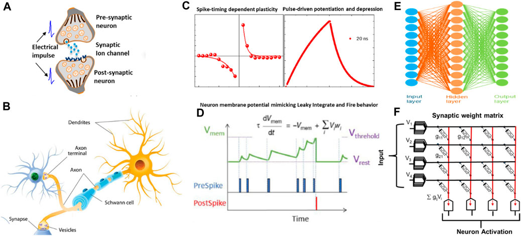
Figure 1. Schematic representation of a biological neural network and its electronic counterpart. (A) A biological synapse and it is response to electrical impulses arriving from the neurons. (B) A biological neuron cell body. (C) Synapse and (D) neuron characteristics. The neuron activation is influenced by its membrane potential, with multiple incoming spikes accumulating and increasing the potential to eventually cross a threshold and fire. These dynamics can be described using a leaky integrate-fire (LIF) neuron model. Neurons are interconnected by synapses, which in electronic circuits can be integrated into crossbar devices with multiple, programmable conductance states. Spike timing dependence plasticity (STDP) and pulse driven potentiation and depression of a synapse help to obtain bio-plausible learning based on synaptic plasticity. (E) A schematic of a neural network and it is hardware implementation in (F) crossbar arrays of synaptic weight elements and neurons.
One key challenge of analog memory, however, is reproducibility and retention of the intermediate states, especially in scaled devices. Due to inherent randomness in domain switching in ferroic devices, we observe a finite distribution of intermediate states under identical pulse programming condition that restricts their bit resolution. At room temperature, higher mobility of ferroic domains together with other defect related effects like movement of trapped charges and vacancies thus make control of analog states even more challenging. At deep cryogenic temperature, on the other hand, lack of thermal energy makes the domain rotation more restricted leading to less bit flips and effectively more control over the intermediate mixed domain states in the ferroic devices. In previous works, with ferromagnetic half-metal-based spin-valves (Majumdar, 2006; Majumdar, 2012b), and magnetic tunnel junctions (MTJ) (Garcia, 2004), sizable resistance switching effects were observed at 4K that decayed substantially with increase in temperature. Even with higher spin-polarized electrodes (Majumdar, 2008; Angervo, 2022), no performance improvements at 300 K were observed. Better performance of such devices at cryogenic temperatures were considered a bottleneck at that time. Now, in the age of high-performance computing, quantum computing and space technologies, when memories working at deep cryogenic temperatures are becoming a major focus for development, these works can provide an important design clue about how we can take advantage of ferroic ordering at low temperatures to design most efficient analog memory and neuromorphic systems.
Physics of spintronic devices for analog memory and neuromorphic computing
Spintronic devices can work as binary resistive switching or memristive devices by storing digital or analog information in their magnetic domain textures (Finocchio, 2021). Among spintronic devices, magnetic tunnel junctions (MTJs) are extensively studied that exhibited reliable memory read and write performances in device dimension down to tens of nanometers (Ikegawa, 2020). MTJs have mostly been used to work as binary memory with high accuracy and thermal stability, ultrafast operation and nearly infinite endurance. However, having controllable multilevel conductance in MTJs is possible based on the controllable switching properties of magnetic moments of the ferromagnetic “free electrode” of an MTJ. In the following sections, we will discuss analog conductivity in spintronic components due to possibilities of information storage based on ferromagnetic domain wall motions. However, before going to the details of multilevel data storage, we need to discuss the common spintronic device architectures, operation principles and potential for integration in a scalable technology and then discuss their properties that makes them suitable as analog memories and synaptic weight elements.
Spin-Valves and Magnetic Tunnel Junctions (MTJs): Spin valves are devices where a non-magnetic thin film is sandwiched between two FM electrodes with different coercive fields HC1 and HC2. When a spin valve is placed in an external magnetic field (H), the magnetic domains of the two ferromagnetic electrodes aligns themselves as per their coercive fields (HC) and their net spin direction become either parallelly (P) or antiparallelly (AP) aligned (as shown schematically in Figure 2A). When H is between the coercive fields of the electrodes, i.e., HC1 <H < HC2, the two electrodes reach an antiparallel alignment. Once H is higher than both the coercive fields, H > HC1 and HC2, the two electrodes attain a parallel configuration. The spin polarized carriers entering the device through one of the FM electrodes leave the device through the counter electrode and in the transit, they face spin dependent scattering within the device. When the two FMs are parallelly aligned, one of the spin directions can pass without suffering significant scattering leading to a device low resistance (ON) state while for antiparallel alignment, both spin directions suffer significant scattering leading to a high resistance (OFF) state, as shown schematically in Figure 2B. The change in resistance arising from this resistance bi-stability gives rise to the giant magnetoresistance ratio (GMR) in spin-valves.
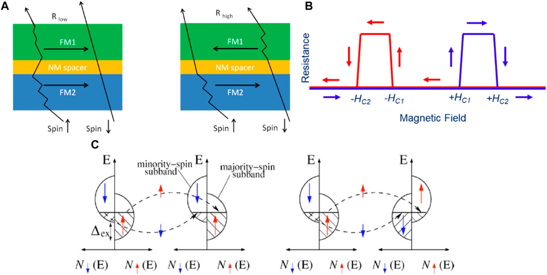
Figure 2. (A) Schematic diagram of a spin-valve architecture for parallel and antiparallel alignments of the two ferromagnetic electrodes showing spin dependent scattering at the two electrodes. (B) Change in electrical resistance of the spin valve due to forward and reverse sweeping of the magnetic fields. (C) Schematic diagram showing spin polarized tunneling of carriers between the two ferromagnetic electrodes with different spin resolved density of states. Adapted from Majumdar 2017, 2018a.
The two FM electrodes inject and detect spin polarized carriers while the non-magnetic spacer decouples the two FM electrodes to ensure independent switching of their magnetic moments. Simultaneously, the spacer should allow unhindered transport of spin polarized carriers. Based on the applied magnetic field, electrical resistance of a spin valve switches between high and low resistance states leading to GMR effect. GMR is defined in Equation 1, where the Rhigh and Rlow is the high and low resistance of the spin valve respectively. A magnetic tunnel junction (MTJ) is a similar architecture as a spin valve, however the non-magnetic spacer in an MTJ is an ultrathin layer of an insulating material (typically <5 nm) through which spin polarized carriers can quantum mechanically tunnel from one electrode to the counter electrode (Figure 2C). The magnetoresistance, thus obtained in an MTJ, is known as tunneling magnetoresistance (TMR). In an MTJ, one electrode’s magnetization is generally fixed known as the pinned layer while the other electrode’s magnetization can rotate freely. This layer is called free layer. In Jullier’s formalism (Julliere, 1975), TMR is defined as
In this formalism, it is assumed that spin-polarized carriers travel from one spin polarized electrode to the other without suffering any spin flip and P1 and P2 represent spin polarization of electrode 1 and 2, respectively. P is defined as
where N(↑) and N(↓) represents density of states at the Fermi level of the up (↑) and down (↓) spin carriers. TMR can also be calculated using the tunneling currents, as shown in Eq. 4, where G↑↑ and G↑↓ represent the junction conductance for the parallel and anti-parallel configuration of the electrodes respectively,
However, it is important to note that in all these formalisms, only the effect of the electrodes have been considered. In reality, the interface between the electrodes and the barrier plays a vital role (Majumdar, 2011; Majumdar, 2018a). Spin scattering, trapping, filtering effects at the interfaces are significant in most practical devices and often determine the critical parameters like device performance over large temperature range, reliability, endurance, yield, etc. Also, for multilevel memories, internal magnetic domain structures of the ferromagnetic thin films, based on their fabrication processes, substrate-induced strain states etc. need to be analyzed carefully. Additionally, based on the magnetic memory component architecture, like the spin-transfer-torque MRAM (STT-MRAM), spin-orbit-torque MRAM (SOT-MRAM) or magnetic nano oscillators (Figure 3), different readout current and switching functionalities can be obtained.
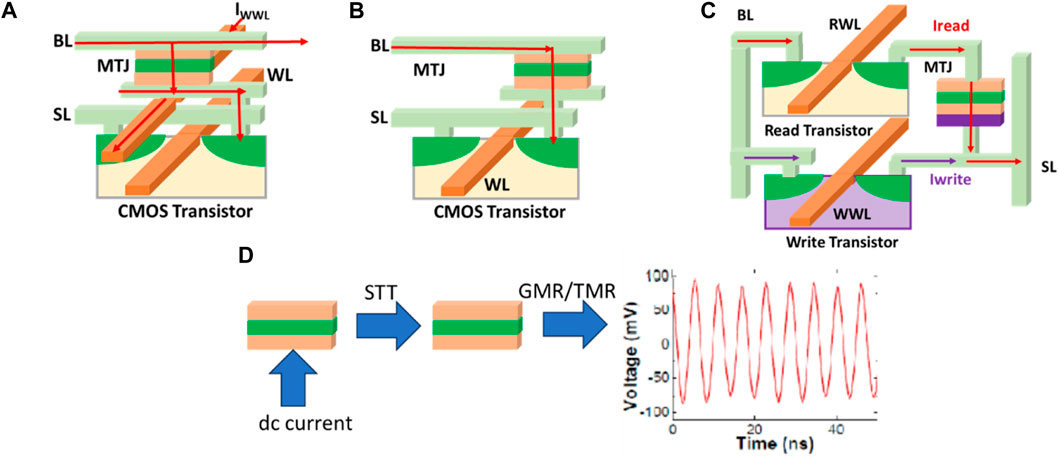
Figure 3. Schematic diagram of different MRAM structures and their operating principles. Schematics of (A) conventional MRAM architecture where magnetic field is used for writing, (B) spin-transfer-torque MRAM where spin polarized current is used for writing (C) and spin-orbit torque MRAM (SOT MRAM) where two separate read and write paths are used and (D) spin-toque nano oscillators (STNO) where a dc current causes precision of the magnetic layer producing spin-transfer torque which upon passing through a GMR/TMR layer produces an oscillating voltage.
Spin-transfer torque MRAM (STT-MRAM): One of the most common spintronic memory components is STT-MRAM. STT magnetization switching, first reported by Berger (Berger, 1996) and Slonczwski (Slonczwski, 1996), arises due to an interaction between magnetization and a spin-polarized current. Here, an exchange of angular momentum between the spins of local magnetic moment and free electrons passing through MTJs gives rise to large magnetoresistance (MR) effect, as shown in Figure 3B. When the two electrodes switch from AP to P configuration, electrons flow from the pinned layer to the free layer. Electrons passing through the pinned layer have the same spin direction as that of the magnetization in the pinned layer and therefore the current is spin polarized. This spin-polarized current exerts STT on the magnetization of the free layer, forcing the magnetization of the free layer to switch. In the reverse switching process, electrons flow from the free layer to the pinned layer. When the electrons pass through the free layer, the electrons with the same spin direction as that of the magnetization in the pinned layer pass through, however, the electrons with the opposite spin direction are reflected at the boundary of barrier and the pinned layer and injected back into the free layer. This reflected current exerts STT on the magnetization of the free layer, and eventually switch the magnetization of the free layer. STT switching on all-metallic spin valve structures with a Cu spacer was reported by Katine et al. (Katine et al., 2000) rather than the MTJs with MgO barrier. The critical properties for operational suitability of an STT-MRAM cell for a particular memory design and node are its resistance, TMR value, switching current and thermal stability. One key challenge for STT-MRAM being the simultaneous achievement of low switching current and high thermal stability (Kawahara, 2012).
Spin-orbit torque MRAM (SoT-MRAM): In a spin-orbit-torque MRAM (SOT-MRAM) cell, the main mechanism is the spin–orbit torque (SOT) working on the principle of spin hall effect. In SOT MRAM technology, a charge current passing through the heavy metal electrode of the MTJ results in spin accumulation in the free-layer of the MTJ due to the spin-orbit interaction. This causes reversal of the free-layer magnetization to either P or AP state, based on the current direction relative to the free-layer easy axis. SOTs unique switching mechanism is reflected in an advantage over STT-MRAM cell due to its separate paths for read and write operation, as shown in Figure 3C. These paths can be optimized independently leading to the possibility to get improvement in write current and write latency in SOT-MRAM cell. Moreover, SOT-MRAMs show more symmetric write operation due to its spin hall effect switching mechanism, compared to STT-MRAM and offer a lower resistance write path than STT-MRAM to allow faster write operations without effecting dielectric breakdown of SOT-MRAM. The transient analysis at the cell level shows pulse width of 5 ns can be adopted for both STT and SOT to work in the precisional regime. STT-MRAM architecture is nearly 50% area-efficient and 74% leakage power-efficient, compared to SOT-MRAM. However, SOT-MRAM cells are 4× faster and more reliable in terms of read disturbance and dielectric breakdown compared to STT-MRAMs. At the architectural level SOT-MRAM found to be performing more efficiently than the STT-MRAM in terms of read/write energy, read/write latency at the expense of marginal increase in chip-area and leakage-power dissipation (Saha, 2022).
Spin-torque Nano-oscillators (STNO): While the previously discussed MRAM cells can serve excellently as electronic synapses due to their memory properties arising from FM domain structures, other spintronic structures can provide biological neuron-like functionalities (Torrejon, 2017). Spin-torque nanoscale oscillators (STNO) are junctions like spin-valves or MTJs that combine STT and GMR or TMR effects (schematics shown in Figure 3D) to produce oscillating outputs. An injected dc current through the MTJ stack, turns the output current into spin polarized current, that generates the magnetic excitation modes of the free FM layer due to STT. This magnetization dynamics is converted into voltage oscillations utilizing GMR or TMR effect, thus producing an oscillatory electrical signal. The electrical signals are directly linked to the dynamics of the magnetization of the free FM layer and to the MR properties of the junction stack. Magnetization precision frequencies may vary from hundreds of megahertz to several tens of gigahertz resulting in radio-frequency oscillations of up to tens of millivolts, that can be detected by measuring the voltage across the junction. STNOs are ultra-small footprint devices where the lateral size can be scaled down to 10 nm limiting the power consumption to 1 μW (Sato, 2014). As additional advantage, STNOs are tunable with a rate depending on the magnetic mode (considered from 10 MHz/mA up to 1 GHz/mA) and agile (from 1 ms down to 1 ns relaxation time), CMOS compatible and radiation hard. These specificities make them promising candidates for integration in future radio frequency and space electronic systems. Like the frequency of biological neurons, STNO frequencies are highly sensitive to the magnetization dynamics of neighboring oscillators that are coupled to them (Slavin, 2009; Housang, 2016). Finally, the fabrication process for STNO technologies is identical to the STT-MRAMs, making it possible to fabricate the neurons and synaptic devices in same process steps (Grimaldi, 2014), which is of vital importance for reducing fabrication complexity and cost.
Physics of ferromagnetic materials for cryogenic analog memory and neuromorphic computing
The field of spintronics witnessed many fascinating materials and device architectures exhibiting novel physics that lead to miniaturization of computer memories to an unprecedented level. Introduction of semiconductors in the field of spintronics has also substantially contributed to versatile multifunctional spin devices for future memory and logic operations. In this section, we discuss the sensitive and complex world of magnetic domains in thin FM thin films that need to be properly understood and controlled in order to implement them in memory and neuromorphic devices, particularly when they are used in more demanding applications where maintaining data integrity is essential.
Magnetic domain and domain dynamics: All the synaptic and neuronal functionalities like linearly programmable synaptic plasticity, long and short-term potentiation and depression (LTP, STP, LTD, STD, respectively), LIF neuron firing and recovery etc. depend strongly on the magnetic and magneto-transport properties of the FM material. To have an in-depth understanding of MR effects, we have to focus on the spin structures at the nanoscale, which includes domain walls, vortices, skyrmions etc. (Malik, 2020). These complex spin structures arise due to the competition between different energy contributions such as magneto-crystalline anisotropy, magnetoelastic coupling, shape-induced anisotropy or dipole interactions in magnetic materials. Magnetic domain structures and their dynamics is of vital importance for controlling analog memory programming and data retention in spintronic memories. Based on magnetic thin film properties, such as strain, microstructures, grain and phase boundaries etc., magnetic domain structures can vary greatly opening a vast design space for proper control of domain dynamics for their application in memory and neuromorphic hardware. As an example, we focus on half-metallic manganite thin films of La0.67Sr0.33MnO3 (LSMO) (Majumdar, 2013) and evaluate the role of different fabrication parameters, such as substrate-induced strain, temperature, growth rate etc. on the magnetic domain structures and their proper control.
Magnetic domain configuration of a FM thin film depends strongly the balance of the anisotropy energies, as mentioned above. Strain on the crystal lattice is one the most critical factors in determining domain configuration. Magnetoelastic effects associated with substrate induced compressive strain results in perpendicular magnetic anisotropy in FM thin films (Wang, 2014; Wang, 2018). From the measured magnetization vs magnetic field (M-H) curves and magnetic force microscope (MFM) imaging, magnetization reversal at 4 K in LSMO nanowires was shown-by Malik et al. and the effective magnetic anisotropy constant (Keff) was calculated (Endo, 2010). With decreasing temperature, Keff increases indicating the enhancement of the magnetoelastic energy at low temperature. Magnetic domains of LSMO thin films are found mobile at 300 K, that eventually settles into a labyrinthine-like pattern. However, at 4 K, they enter a randomly distributed state, that is attributed to the larger saturation magnetization (MS) and Keff at low temperature. Domain imaging showed how domain reversal at different magnetic fields occur at low temperatures. For the external magnetic fields exceeding 0.7 T, the LSMO was fully saturated, exhibiting a mono-domain state. At 0.5 T, domains with downwards magnetization started to nucleate. As the field further decreases, the down domain size expanded further, and the volume ratio of up domains shrank. In the absence of external magnetic field, almost equally populated up and down domains were formed, confirming the demagnetization state. In a La0.5Sr0.5MnO3 thin film, at the boundary of ferro- and antiferromagnetic phases, Majumdar et al. (Majumdar, 2024) measured magnetization reversal using photoemission electron microscopy (PEEM), with magnetic contrast from x-ray magnetic circular dichroism (XMCD), known as XMCD-PEEM. These data provided an in-depth understanding of the magnetic domain structures and their reversal at cryogenic temperatures. As shown in Figure 4, due to sweeping magnetic field, XMCD-PEEM image revealed how the magnetic domain rotation happens in La0.5Sr0.5MnO3 thin film at 40 K. The full red or blue states represent magnetic saturation in up or down direction i.e., all electronic spin states being aligned parallel to the external magnetic field direction. Upon withdrawing the field, the saturated state continued in these films, representing the non-volatility of the “1” and “0” states. Application of fields of a few mT resulted in mixed domain phase, showing how the intermediate states appear in the film and their evolution happens due to increasing field strength. The dynamics of the up and down polarized magnetic domains were studied by sweeping the magnetic fields from positive to negative value and back. The red part in the image (A), representing the fully up-polarized domains, remained in their programmed state when the magnetic field in withdrawn (B). Upon field reversal, white parts started to appear (C-D) showing the mixtures of orientations leading to nearly depolarized states in some local areas while the appearance of the blue parts represented existence of some down-polarized domains in the predominant up-polarized matrix. Upon increasing the reverse field strength, the blue area started increasing, eventually consuming the entire area (E-I). The stability of these domains was checked by imaging the domains over extended period after withdrawing the magnetic field and interestingly it was found that some domains are more pinned and can retain their orientation for hours after removing the field. All the intermediate states were found reproducible. However, the magnetic history of these samples was important in exactly determining their mixed polarization states.
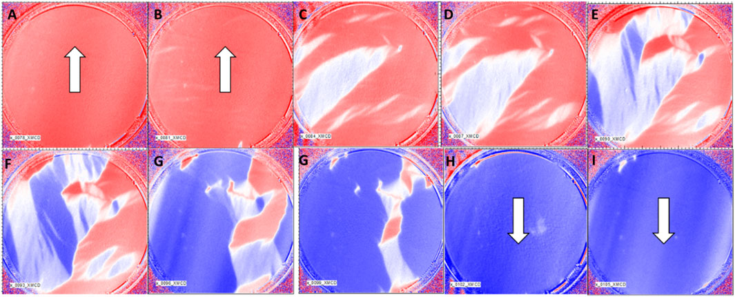
Figure 4. Magnetic domain imaging using photoemission electron microscopy (PEEM), with magnetic contrast from x-ray magnetic circular dichroism (XMCD) technique (XMCD-PEEM) at 40 K. The images were taken from La0.5Sr0.5MnO3 thin films of 20 nm thickness. In order to study the local magnetic switching of the magnetic domains in the films, XMCD-PEEM images were recorded in a varying magnetic field between +10 mT (A) to −10 mT (I). The results show that at saturated magnetization states, the samples are homogeneously magnetized. However, when the in-plane magnetic field was varied between the saturation values, a clear domain wall formation between parallel and antiparallelly aligned domains of the LSMO film surface was seen. With further increase of magnetic fields, more and more domains changed their orientation resulting in sharp change in magnetic contrast image. Adapted from Majumdar 2024. (A–F) represents XMCD images under different magnetic fields showing gradual magnetic domain rotaion.
In order to address the finite retention of mixed polarization phase, domain reversal dynamics and their stabilization needs more in-depth study and analysis. Clarification of domain pinning mechanism through naturally occurring or artificially engineered pinning sites is an important subject that needs discussion in this direction. Lecoeur et al. (Lecoeur, 1997) studied the effect of epitaxial and polycrystalline films on the magnetic domain reversal and MR effects of FM thin films and their results demonstrate that the presence of microcracks can effectively manipulate the domain structure in LSMO films. In the polycrystalline thin films, formation of domain structures is largely influenced by the grain structure. The average coercive field Hc was found to be more than twice as large as that of a single crystal film.
A Kerr-microscope study of the magnetic thin films showed that in polycrystalline films the grains switch mostly independently; each in a narrow range of fields but the distribution of switching fields becomes quite large while considering macroscopic area leading to a higher coercivity of the film. In the smaller grains, M is mostly uniform, however, in larger grains, domain walls were found to be involved in the reversal process. Effects of grain-boundaries on the magnetoresistance properties of perovskite manganite films was also studied by Gupta et al. (Gupta, 1996), that showed large MR over a wide temperature range down to 5 K can be obtained in polycrystalline films, which can be explained in terms of switching of magnetic domains in the grains and disorder-induced canting of Mn spins in the grain-boundary region. However, in epitaxial LSMO films, magnetization occurs by rotation and domain-wall movement over large areas unlike in the polycrystalline samples. A domain wall can cross a grain-boundary and its motion can get impeded by surface defects such as scratches. Large low-field MR in polycrystalline films is a result of tunneling of electrons through grain boundary.
Fabrication process control for reliable analog operation
Magnetic domain structures, their motion and stability can be engineered through control of nanofabrication process parameters. For instance, in LSMO films, prepared by pulsed laser deposition technique, substrate-induced strain and different deposition parameters can modify the high and low angle grain-boundaries (Figure 5) affecting the magnetization reversal dynamics and analog response (Majumdar, 2012a). For instance, films grown on single crystal MgO substrates contained higher number of structural defects compared to those on SrTiO3 (STO) and NdGaO3 (NGO) substrates leading to higher polycrystallinity in the films. Also, lower deposition rate and thicker films resulted in more polycrystallinity and grain boundaries that caused broader magnetic transition (Figure 5), deposition parameters are shown in Table 1. This was attributed to large lattice mismatch (9%) between the substrate and the LSMO film. The LSMO films deposited on STO and NGO showed sharper magnetic transition due to lower effect of substrate induced strain. The MR effect measured up to 300 mT field, clearly showed two contributions, one due to grain boundary tunneling and the other due to colossal MR effect. In addition to the substrates, lower pulsed laser frequency, higher deposition temperature and increasing film thickness led to more structural defects in the films, causing broader magnetic transition.
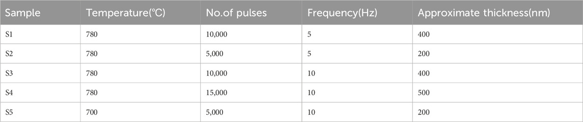
Table 1. Sample numbers, deposition parameters and approximate thicknesses (from Majumdar, 2012a).
Figure 5. X-ray pole figures of the (1 1 0) reflection at 2θ = 32.76° of as deposited LSMO films deposited on MgO, STO and NGO substrates using deposition parameters shown in Table 1. Reproduced with permission from Majumdar 2012a.
Hawley et al. (Hawley, 2000) studied the stability of the magnetic domain structures in LSMO films grown at 750°C and 800°C. Scanning tunneling and magnetic force microscopy was used to image the film microstructure and domain structures as a function of in-plane magnetic field strength. With increasing field strength, the maze-like domain structures in the film were found to become striped domains with reduced out-of-plane magnetization and decreased wall spacing that confirm parallel alignment of in-plane spin polarization. After removal of the field, the stripe domains remained, however, the wall spacing, and z-component of polarization was found to return to the original value. It was found that magnetic structure of the film with a thin insulating cap layer was reversible, suggesting pinning of the domain walls by the capping layer.
Spintronic synapses: Utilizing this magnetic domain formation and their reversal dynamics in ultrathin FM films, spintronic components with analog and multiple bit storage elements and synaptic weight elements can be fabricated. Previous studies reported that magnetic devices can have promising performance as memristors by storing analog information in their magnetic domains and textures (Sharad, 2012). A spintronic memristor was shown by Wang et al. (Wang, 2009) based on magnetic domain wall displacement of a (Yamaguchi, 2004) in a spin-valve. Also, domain wall motion based memristors has been experimentally demonstrated in MTJs (Chanthboula, 2011; Lequeux, 2016). Position of the domain walls in these spintronic memristors determine the lower or higher resistance states (Grollier, 2003). SOT switching in an antiferromagnet–ferromagnet bilayer has also demonstrated memristive behavior (Miron, 2011; Liu, 2012; Fukami, 2016a; Fukami, 2016b). The variation in switching currents among the magnetic domains with varying exchange-bias magnitudes and directions at the antiferromagnet–ferromagnet interface results in memristive behavior in these structures (Kurenkov, 2017). Thus by harnessing the materials physics, one can design programmable domain features and dynamics. (Marcovic 2020).
Spintronic neurons: In addition to the MTJ-based technology, other types of neurons, based on domain-walls and skyrmion-based neurons have also been reported in literature. Sharad et al. proposed magnetic solitons (Sharad, 2012), that can be manipulated and moved over large distances with spin torques and spin–orbit torques (Yamanouchi, 2004; Thomas, 2010; Woo, 2016). These devices take advantage of the fundamentally stochastic nature of the domain wall motion, their depinning and magnetic nanotextures (Hayashi, 2006; Hayward, 2015; Zázvorka, 2019). Simulations show that cumulative nature of domain wall motion or skyrmion accumulation (Li, 2017; Pinna, 2018; Zázvorka, 2019) and switching can give rise to LIF kind of neuronal activity.
In a recent work, Yang et al. (Yang, 2021) studied a complete spin-based integrated neural network by electrically connecting spin synapses (named, spin-S) and spin neurons (named, spin-N) and evaluated their performance for a pattern classification task, as shown in Figure 6. A stack structure of MgO/CoFeB/W was used in the experiments and the Hall resistance of the device was determined by the position of the current-driven DW motion. A very linear and symmetric weight update in these spin-S devices were attributed to the uniform shifts of the DW due to application of the pulse train of ±12 V of 50 ms duration with a y-axis magnetic field of −80 Oe. It was further observed that a precise weight can be achieved by means of the stripe domains, where domain width can be controlled by material parameter engineering, including perpendicular magnetic anisotropy, dipole energy, Dzyaloshinskii–Moriya interaction, and pinning densities. A high classification accuracy of over 93% was achieved only using the optimization of spin-S and spin-N components without further support of additional software or circuit optimization, proving in terms of synaptic weight update linearity, symmetry, and stability, spintronic components can achieve quite promising performance.
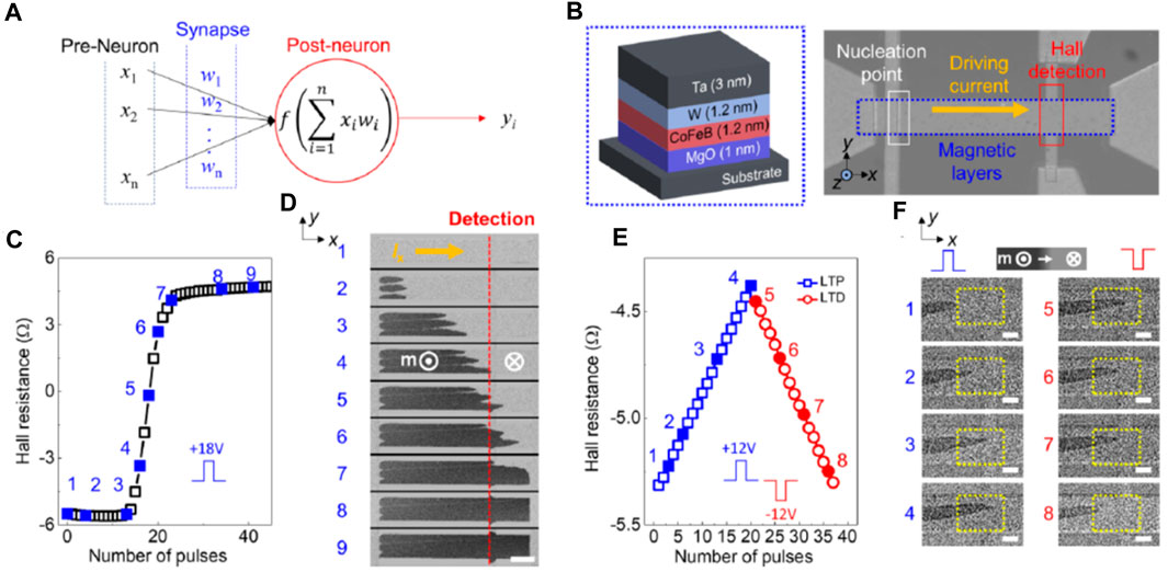
Figure 6. Representative spin neuron and weight functions. (A) Schematic of the perceptron, part of the artificial neural network; (B) schematic of the MgO/CoFeB/W structure and an optical image of the patterned Hall bar device with the measurement configuration; (C) representative Hall resistance determined by the position of the current-driven DW; and (D) corresponding MOKE images for each state (marked as blue numbers). The light and dark gray colors in the MOKE images represent the +z and −z magnetization domains, respectively; (E) typical LTP/LTD functions of the Hall resistance modulated by potentiation/depression training pulses ±12 V in amplitude with a fixed pulse width of 50 ms; (F) corresponding MOKE images for each state (marked by blue numbers for potentiation and red for depression). (Figure reproduced with permission from Yang, 2021).
Böhnert et al. (Böhnert, 2023) have demonstrated weighted spin torque nano oscillator (WSTNO) as a programmable building block for neuromorphic computing. The WSTNO circuit used two types of spintronic devices, MTJs as synapses and non-linear STNOs acting as a neuron. The nonlinear output based on the weighted sum of the inputs is demonstrated using three MTJs. The STNO shows an output power more than 3 μW and frequencies of 240 MHz. Both types of MTJs are fabricated using single fabrication process, compatible with monolithic CMOS integration, paving ways for complex neuromorphic computing systems.
Physics of ferroelectric devices for neuromorphic computing
Most of the materials and device physics related to domain formation and reversal for ferromagnetic components can be almost directly applied to ferroelectric components, except for the fact that ferroelectric devices being charge based devices, does not possess infinite endurance, especially in scaled ultrathin capacitor-based structures. However, ferroelectric devices bring the advantage of compatibility with existing CMOS fabrication facilities, especially high-k oxides like hafnia-based systems and large On/Off resistive switching, making their control over analog states more robust and reproducible. Additionally, the rich physics of FE polarization switching, polarization retention and relaxation in FTJ and FeFET architectures opens an avenue for designing dense, low-power, analog spiking neurons and synapses, similar to their biological counterparts with minimum number of components.
FeRAM, FTJs and FeFETs:
Figure 7 shows schematics of different ferroelectric device architectures and their working principles. Traditional FeRAMs consist of a FE capacitor in series with a MOS transistor that stores the memory in terms of FE polarization charge with the MOS transistor acting as a switch. Although a matured technology due to its robust operation, high operating voltage, destructive readout and large footprint of FeRAMs pose challenges for their integration in dense memory arrays.
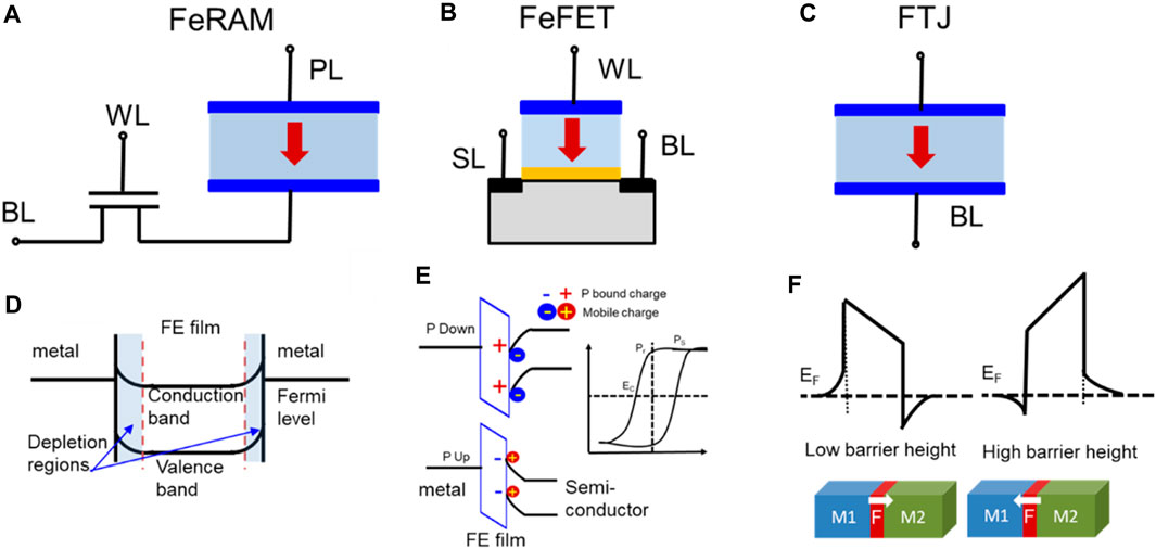
Figure 7. Schematics of Ferroelectric memory devices consisting of (A) one-transistor-one-capacitor (1T1C) cell known as FeRAM where the non-volatile data storage takes place in the ferroelectric capacitor while the MOSFET acts as a switch, (B) one-transistor FeFET memories where the ferroelectric layer is integrated in the MOSFET gate stack. In FeFETs FE polarization charge determines devices On, Off and non-volatility of polarization charges determines memory properties and (C) an FTJ, analogous to an MTJ, where change in the direction of FE polarization in the ultrathin FE tunnel barrier, sandwiched between two metals with different work functions, causes an asymmetric barrier potential. This results in modifications of barrier heights for the tunneling electrons for the two-polarization direction, causing resistive switching. (D–F) Schematics of the corresponding device band diagrams. Figure reproduced from Majumdar 2022a.
Ferroelectric tunnel junctions (FTJ): In an FTJ, analogous to an MTJ, two different metal or semiconducting electrodes are separated by an ultrathin layer (1–5 nm) of FE film. However, in an FTJ, the barrier plays the major role as the FE barrier is the active component unlike the passive barrier in an MTJ. In a sweeping electric field, the FE polarization direction in the barrier switches between up or down directions depending on the electric field polarity. Metallic electrodes in FTJs provide the mobile charge carriers to screen the FE bound polarization charges providing the stabilization of FE polarization. Based on the direction of FE polarization in the tunnel barrier, charge carriers are either accumulated or depleted from the FE-electrode interface. Junctions with different metal electrodes on either side of the FE causes an asymmetric screening effect, producing an asymmetric barrier potential in the FTJ. Thus, polarization switching induced modification in the mean tunnel barrier height causes the electrical resistance of FTJs to switch between high and low states. This results in device Off and On states, respectively and this phenomenon is known as the tunneling electroresistance (TER) effect (Kohlstedt, 2005; Tsymbal, 2006; Gruverman, 2009). TER is defined as,
Where Rhigh and Rlow are the junction resistance in device Off and On states, respectively. In earlier reports, FTJs with two metal electrodes are mainly reported. However, studies found that one semiconducting electrode at one end of the FE is capable of leading to larger resistive switching effect due to the Schottky barrier formation at the FE/semiconductor interface (Majumdar, 2018b; Majumdar, 2019a). When the polarization direction moves away from the semiconductor interface, the formed Schottky barrier adds to the effective barrier width, in addition to change in barrier height of the FTJs, causing a larger TER effect.
Besides the crucial role of electrodes in determination of barrier height asymmetry (Maksymovych, 2009), charge screening at the electrode-FE interface also affects the long-term stability of FE polarization that determines the non-volatile and volatile data retention of the FTJs. For an electronic synapse, stability of FE polarization can affect the long or short-term potentiation (LTP, STP) and depression (LTD, STD) characteristics. Similar to MTJs, FTJs were mostly used as a bistable resistive switching memory. However, Chanthboula et al. (Chanthboula, 2011) first demonstrated that FTJs not only work as a binary memory, but programmable control of partial switching of FE domains can lead to multiple intermediate resistance states. In large area devices, multiple FE domains are formed to maintain an energetically stable configuration. Control of a mixed domain phase in these devices with coexisting up and down domains is therefore comparatively straight forward. However, with device scaling down, number of FE domains involved approach from multiple to a few-domain limit and a precise control over intermediate states becomes a challenge. For devices with ultrathin FE films, another important consideration is the interface quality of the FE films with its electrodes. In oxide FE based FTJs, in addition to the FE polarization reversal induced resistive switching, multiple other conduction phenomenon can be observed such as electric-field-enhanced reversible migration of oxygen vacancies (Garcia, 2014; Qin, 2016), filamentary conduction and so on. Defects inside the FE film and at the interface cause charge trapping sites, which, over multiple field cycling builds up significantly, causing the device to operate with less On/Off ratio and eventually to fail due to breakdown. In neural network applications, especially for DNN training operation, this is a challenge where 109 cycles of on-off cycles are expected from the synaptic weight elements. Therefore, while designing large-scale networks with nanoscale FE memories, control of interface quality and FE domain dynamics, needs to be considered carefully. Also, for synaptic weight elements, switching and relaxation timescales, are of vital importance. A proper design of material stack and device configuration can create an extremely energy efficient and versatile hardware neural network based on FE devices.
Ferroelectric field effect transistors (FeFETs): A FeFET is analogous to a metal-oxide-semiconductor field effect transistor (MOSFET), where the gate dielectric layer of the MOSFET is replaced by a FE material. In a FeFET, an applied gate bias polarizes the FE layer, and the net FE polarization pointing towards or away from the MOSFET channel. With the polarization direction pointing toward the channel, electrons accumulate at the semiconductor-FE interface in n-type semiconductors, causing in increased conductivity in the channel, that leads to the device On state. On the other hand, when the polarization direction points away from the channel, a depletion of electrons at the FE-semiconductor interface causes the drain-source current to decrease and leading to device Off state. For a FeFET with p-type semiconductor channel, a reverse voltage polarity and therefore FE polarization determines the On and Off states.
In order to operate the FeFET with full polarization switching and thus having the full memory window (MW) available, a gate bias higher than 5 V magnitude is generally needed. However, in a CMOS-integrated circuit, one critical consideration is to keep the access transistors small that poses limitation on the maximum available programming voltage. This opens the design space with novel materials, electrodes, designed interfaces and device architecture for maximizing the memory performance within low operating voltage limit. For analog memories, a large number of stable intermediate states are needed using a relatively lower programming gate bias that causes partial polarization rotation of the FE and leaving a mixture of up and down polarized domains in the gate stack. This mixed polarization phase can neither fully accumulate nor deplete the semiconductor channel, causing intermediate conductance levels. One observed challenge for the partially polarized states is their instability in comparison to the fully polarized states. Additionally, there exists a history dependence of the intermediate states that requires different programming and erasing protocols while designing analog memory circuits with the FeFETs.
Physics of ferroelectric materials for cryogenic analog memory and neuromorphic computing
As the most researched CMOS back-end-of-line (BEOL) compatible ferroelectric in the recent times, we discuss the physics of FE Zr-doped HfO2 (HZO) system. However, we also discuss other single and polycrystalline FE material due to lack of enough experimental data on Hafnia-based systems. The origin of ferroelectricity in HZO have been discussed in detail in literature (Kim 2019; Onaya 2019). Here, we focus our discussion mainly on the polarization switching and FE domain dynamics, together with the polarization relaxation mechanism. The transient switching dynamics of FE components decides the synaptic and neuronal functionalities of these devices and therefore it is of vital importance to understand and master their proper control.
Ferroelectric materials belong to the broad class of dielectric materials where a net electric polarization arises due to a broken centrosymmetric phase of the crystal lattice and the net polarization can be switched using an external electric field. The net polarization in a FE material changes non-linearly under an electric field. When an external electric field exceeds a certain field, the net polarization of the FE suddenly increases reaching a saturation polarization (PS) eventually. Upon withdrawal of the electric field, the net polarization is maintained at a non-zero value, called the remnant polarization (Pr). On reversing the polarity of the applied field, the polarization direction rotates to the opposite direction, reaches a zero value at the coercive field (EC) and eventually reaches the negative Ps value. Pr, Ps and EC are the critical parameters for FE materials. When the electric field is high enough to saturate the FE polarization, the P-E hysteresis loop is wider, and the loop is called a FE major loop. However, when the applied field is not enough to reach Ps, the P-E hysteresis loop narrows, leading to a FE minor loop. The trajectories and dynamics of the major and minor loops are vital parameters for designing stable analog operation of the memories. It is found that long-term retention can readily be obtained for a device reaching its FE major loop (Majumdar 2019a). Therefore, depending on the applied programming voltage, pulsing scheme etc., a non-volatile or a volatile memory performance can be achieved.
In FE devices, there are multiple mechanisms in addition to polarization switching that leads to performance degradation. One such effect is imprint, and another is fatigue. When the switching of one polarization direction is more favored compared to the other and the hysteresis loop is asymmetric along the electric field axis, i.e., the +EC and -EC values are different for polarization switching, the FE components are known to have an imprint effect. This is analogous to magnetic exchange-bias effect in FM films. FE-electrode interface and structural defects in the FE play a major role in imprint effect. Fatigue in FE components appear due to repeated switching cycles causing charge trapping, leakage currents or structural degradation in the FE due to bias stress especially arising from high current due to oxygen vacancy movement inside the film. Fatigue results in loss of PS and Pr values. Device endurance properties strongly depend on the fatigue properties. However, devices can sometimes recover from fatigue states upon withdrawal of the field.
Ferroelectric domain dynamics
In polycrystalline ferroelectric thin films, polarization switching is generally inhomogeneous. The switching mechanism can be explained by nucleation-limited-switching (NLS) model (Tagantsev, 2002) where polarization reversal takes place through independent switching kinetics of different areas in the film. The normalized area of reversed polarization, S can be approximated as a function of time t and voltage V as,
assuming a Lorentzian distribution of the logarithm of mean nucleation times (tmean) for each applied voltage pulse V with width Γ(V) and centred at log(tmean(V)). When considering a one-to-one correspondence between the ferroelectric domain configuration and the FTJ resistance R, the fraction of domains with upward polarization (S) and with downward polarization (1−S) can be expressed using a parallel circuit model,
where the lowest resistance ROn and the highest resistance ROff represent fully downward (S = 0) and fully upward (S = 1) ferroelectric states. (Boyn, 2017; Ma, 2020) From the experimental Resistance–Voltage hysteresis loops (Figure 8), the normalized switched area as a function of programming pulse duration can be calculated at different pulse amplitudes by plotting R as a function of pulse duration and by fitting with the NLS model. From the fitted tmean values, it was found in different FE systems (Boyn, 2017; Majumdar, 2021) that the switching time depends exponentially on the electric field as described by the Merz law. (Merz, 1954) Depending on the polycrystalline film morphology (Figure 8), the switching dynamics and mean switching time can be modified and with a proper electric field, the switching time can be as fast as sub-nanosecond, leading to possibility of ultrafast write time in FE memory components. A few reports showed (Park, 2016; Wei, 2022) a 2-stage switching dynamics in ferroelectric HZO, the reason for which was ascribed to either mixture of phases, positively charged oxygen vacancies compensating for the polarization charges or imprint field. This 2-stage switching leads to two different mean switching fields and based on applied field strength or pulse duration, a certain timescale for switching operation can be chosen. In a recent work, Dahlberg et al. (Dahlberg, 2023) showed higher switching speed can be obtained in Zr-rich HZO showing higher anti-ferroelectric phase ensures faster switching speed, however at the cost of lower remanence. As thermal energy assisting domain rotation and oxygen vacancy movements are restricted at lower temperatures, domain dynamics at cryogenic temperatures is expected to be different and need to be investigated in detail for memories and in-memory-computing circuits operating at cryogenic temperatures.
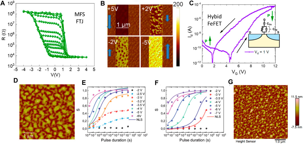
Figure 8. Multiple conductance states due to complete or partial polarization rotation in ferroelectric devices. (A) Memristive behaviour from FTJs upon programming with different voltages. When scanning between −4 V and +4 V, the devices showed large On/Off ratio of >104, however for operation within smaller voltage range, the device started showing reduced resistance switching, indicating partial FE domain rotation. (B) Electrical data of (A) further verified by piezo-force microscope data showing partial domain rotation, shown by bright and dark regions. (C) Analog nature of drain current switching in FeFETs with hybrid FE/DE gate layer. Inset showing the FeFET schematics. (D–G) Polycrystalline ferroelectric morphology dependent domain switching dynamics where low temperature annealing led to bigger crystallites separated by wide grain boundaries, as shown in the image (D) using AFM compared to the film with higher annealing temperature, shown in the image (G). The low temp annealed film domain switching dynamics could only be fitted with nucleation limited switching (NLS) model (E) only when applying larger electric fields compared to the high temperature annealed films (F), concluding microstructure dependence of analog conductance in FTJs. (Figure reproduced from Majumdar, 2019a; Majumdar, 2019b; Majumdar, 2023; Majumdar, 2021).
Fabrication process control for reliable analog operation
Analog operation in ferroelectric components results from gradual domain rotation. This feature can be realized using optimized ferroelectric film morphology or FE device design. In polycrystalline thin films, domain rotation is rather gradual where higher number of grain boundaries and structural defects are present. While this was considered an undesirable aspect for digital memory operation, this has proven to be a more effective way to maintain linearity in weight update in synaptic elements. By modifying substrate-induced strain states (Goh, 2020), crystallization temperature and protocol (De, 2021a) and stack ordering (Migita, 2021), it is possible to have control over polarization switching dynamics which can influence the linearity in weight update from FE components. In a recent report, Arabar et al. reported better control of analog states can be achieved using a FE-DE superlattice structure (Arabar, 2022). Similar conclusion was drawn by Majumdar et al. (Majumdar, 2023) where in 2D semiconductor-based synapses linearity of conductance update was obvious. However, this hybrid stack comes at a price of increased depolarization field, leading to quick decay of conductance states. It was shown through simulation that optimization of the stack by using proper thickness and dielectric constant of DE, depolarizing field can be minimized in these structures to achieve long-term retention (Majumdar, 2023).
Ferroelectric synapses
Different kinds of synaptic plasticity functions like long-or short-term potentiation and depression (LTP, STP, LTD and STD respectively) functions have been demonstrated in ferroelectric devices (Boyn, 2017; Majumdar, 2019a) (Figures 9A–C). In FTJ synapses, the applied voltage pulses were found to align the FE domains in a way that the net polarization value of the FE changes resulting in a momentary increase in post-synaptic current (PSC). Withdrawal of the excitation pulses, especially single pulses coming at sufficient intervals lead to a quick decay of the PSC, resulting in STP and STD. STP or STD arises due to finite retention of intermediate polarization states, i.e., when polarization direction is not in a strictly perpendicular orientation, and lead to the recovery of the initial conductance states. Magnitude, width, and frequency of the excitation pulses can modify the relaxation time period and can turn the STP and STD behavior to LTP and LTD behavior (Wang, 2021). In oxide perovskite FTJs, different STDP learning curves based on designed voltage pulses have been demonstrated through controlled ferroelectric domain dynamics by Boyn et al. (Boyn, 2017) In Hf0.5Zr0.5O2 based FTJs, synapse potentiation and depression and STDP were also demonstrated (Yoong, 2018), suggesting a viable path of fabricating FTJs with good CMOS compatibility.
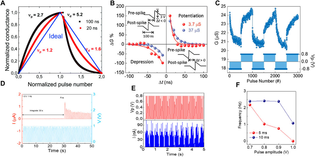
Figure 9. Synaptic potentiation and depression due to different applied pulse trains. (A) Plot of normalized conductance vs normalized pulse number for 100 ns and 20 ns pulse trains in an FTJ synapse device showing improvement in linearity for excitation with shorter pulses. (B) STDP of FTJ synapses when pulses of 3 V amplitude and 100 ns duration was applied with pre and post synaptic pulse delay varying between 100 ns and 20 ns range. (C) Synaptic potentiation and depression due to application of symmetric and identical pulse trains of 0.8 V magnitude. (D) Neuronal leaky-integrate-and-fire (LIF) response from an FTJ showing under excitation with identical subthreshold pulses (of 1 V magnitude), polarization switching happens after accumulating certain number of pulses. (E) oscillatory current response in an FTJ neuron when excited with 0.8 V pulses. (F) neuronal current oscillation frequency depending on excitation pulse magnitude.
It has often been seen that linearity and symmetry of synaptic conductance has a clear trade-off with the dynamic conductance range. Within a limited conductance range (Majumdar, 2021; Majumdar, 2022b), it is possible to achieve better linearity in weight update compared to when using a larger dynamic range. This can be due to use of programming pulses of certain magnitude or width. In FE devices, large dynamic range is generally associated with higher amplitude or longer duration pulses that lead to more drastic rotation of polarization initially followed by saturation which inhibits the possibility of linear weight update. However, in a FeFET, control over channel conductance for larger dynamic range and linearity is more probable compared to FTJs due to the additional advantage of large On/Off switching of MOSFETs. In such systems even, linearity is mostly limited to application of continuously increasing pulse amplitude that makes the driving circuit complicated.
A single FeFET synapse, based on ferroelectric hafnia and integrated in a 28 nm HKMG technology was shown by Mueller et al. (Mueller, 2012), where a non-volatile, gradual switching of the FE layer was used to continuously tune the conductivity of the transistor channel. This continuous change in conductivity led to the possibility of synaptic weight update over multiple switching pulses leading to synaptic potentiation and depression. Lederer et al. (Lederer, 2021) demonstrated that hafnia based FeFETs are extremely promising as synaptic weight elements that can find application for hardware acceleration of neural networks. Utilization of increasing magnitude or increasing pulse width pulse schemes in Si- or Zr-doped HfO2 based FeFETs could achieve a linear weight update in devices as small as 100 × 100 nm2. From the design point of view, smaller grain sizes were found suitable for further device scaling and therefore, microstructure engineering by varying grain size and crystallographic orientation will be of major importance for scaled ferroelectric synaptic devices. For analog operation, devices with larger channel lengths and widths are generally suitable as they involve a large number of FE domains where a mixed polarization phase is easier to achieve. In FeFETs, voltage pulses are applied either at the gate and/or source-drain terminals that switch the polarization of the FE layer in a non-volatile manner, tuning the channel conductivity gradually. Progressively increasing gate pulse amplitude leads to gradual switching of FE layer in the gate stack in the multi-domain devices, turning an initially high-Vth state into a low-Vth state. STDP was also exhibited by FeFETs (Mulaosmanovic, 2017). A multilayer perceptron based deep neural network accelerator with FeFETs as the analog synapses were demonstrated by Jerry, et al. (Jerry, 2017) A 5-bit symmetric potentiation and depression behavior with a 45x tunability in conductance range was reported using 75 ns pulses. A transient Presiach model predicted the minor loop trajectories and Pr values for arbitrary pulse width, amplitude, and device history. A benchmarking done on on-chip learning accuracy for an affordable area, latency and energy overhead showed a FeFET based synaptic core could achieve a 103 to 106 times acceleration in online learning latency over multi-state RRAM based analog synapses. Hybrid FeFETs using composite dielectric (DE)-FE gate stack has shown superior performance in achieving multiple intermediate conductance states with high reproducibility due to depolarizing field induced division of larger domains into smaller domains and voltage division across the DE-FE gate stack (Arabar, 2022; Majumdar, 2023). De et al. (De, 2021a) has shown effect of device-to-device (D2D) and cycle-to-cycle(C2C) variation on neural network performance based on the Fe-FinFET platform. The results show that stochastic D2D variation gets compensated during online training and shows almost no effect on the training accuracy, however, a substantial drop in inference accuracy can occur due to systematic degradation of device retention in analog neural networks. Quaternary and binary neural networks with FefinFETs as synaptic devices however demonstrated excellent tolerance toward the stochastic and systematic D2D variations arising from coexisting paraelectric and FE phases due to incomplete crystallization of HZO (De, 2021b).
For large-scale circuit integration of ferroelectric memories, compact modelling of the device performance is of major importance. While several analytical models for the polarization switching in FE materials exist, their parameters are either experimentally challenging to extract, or lacks physics-based definitions, or are computationally very demanding. A few recent works (Lederer, 2023; Paasio, 2023), have shown Spice and Verilog-A compatible Jiles-Atherton model can be implemented for modelling FE capacitors that provides highly computationally efficient prediction of intermediate states by transient switching.
Recently, nearly ideal linear weight update from HZO based devices have been shown at cryogenic temperatures (Bohuslavskyi, 2024). It is shown that temperature is an additional parameter controlling the FE domain dynamics and below 100 K, a significant improvement in potentiation and depression linearity can be obtained, especially at higher operating frequencies. Lack of thermal energy and frozen charge defects at cryogenic temperatures can lead to improved control over FE domain dynamics, leading to the possibility of high accuracy in-memory-computing below 100 K.
Ferroelectric neurons
Polarization switching in FE thin films is accumulative in nature, especially when excited with pulses of amplitude smaller than coercive voltages, and this feature is a promising way to design area and resource efficient LIF neuronal components. A threshold switching behavior has been introduced in FTJs and FeFETs to mimic neuronal firing activities (Figures 9D–F). In nanoscale FeFETs with Si-doped HfO2 as the gate material, two key neuronal dynamics such as integration of action potentials and the subsequent firing have been demonstrated. Firing was optimized in these devices by designing specific electrical excitations that can induce a particular NLS kinetics in the FE layer. Depolarizing field (Edep) determine the relaxation of polarization charges in a FE film and therefore Edep could be engineered to tune the firing frequency, arbitrary refractory period and the leaky effect of the neurons. Due to the stochastic nature of switching of single domains, an inherently stochastic nature of switching can be obtained in scaled FeFETs and therefore it is easy to design FeFET-based single cell LIF neurons. One such report is from FeFETs with 30 nm channel length and 80 nm width (Mulaosmanovic, 2018) highlighted the possibility of advanced downscaling of neuron circuits that can significantly reduce the complexity of fabrication and cost of neuromorphic architectures.
In FTJs, LIF neuronal functionalities have been reported by Majumdar et al. (Majumdar, 2019b) by modifying depolarization field strength of the junction. High depolarization field, arising from incomplete screening of polarization charges, results in quick relaxation of polarization leading to volatile switching property. Therefore, when a junction is excited with subthreshold pulses, few domains start to rotate polarization and the number of switched domains keep on accumulating until the net polarization switches, mimicking threshold switching of membrane potential of biological neurons leading to integrate-and-fire function and eventually getting back to its rest condition mimicking reset behavior due to quick relaxation of polarized domains. Engineered depolarizing field in these FTJs by varying charge-carrier densities in the bottom semiconducting electrode, a switch-over from NVM to volatile switching was obtained (Majumdar, 2019b) leading to the possibilities of fabrication of synapses and neurons with same process steps, minimizing the fabrication complexity and cost. By modifying pulse amplitude, frequency and width, it is possible to tune the accumulation and firing frequency and also the leaky behavior. Inherent stochasticity in domain switching helps in replicating the stochastic firing behavior of biological neurons.
Cryogenic memory based on ferroic ordering
Most of the cryogenic characterizations from FE devices are reported from perovskite FE based FTJs like BaTiO3, PbTiO3, Pb1-xZrxTiO3 (PZT) etc. (Garcia, 2014; Qin, 2016; Tan, 2019) that shows FTJ performance stability is greatly improved at low temperatures with large On/Off ratio, stable data retention and low leakage currents. However, the switching voltage increases due to cool down that was considered as a drawback. For HZO, most of the available results are from room temperature since developments on HZO are mainly driven from industrial demand side. A few recent reports have studied temperature-dependent studies on Si-doped hafnia (Park, 2018; Wang, 2020b) or HZO capacitors (Wang, 2019) with superconducting NbN electrode (Henry, 2019) and with commonly used TiN electrodes down to 4 K (Hur, 2021). The report by Hur et al. (Hur, 2022), showed excellent endurance performance of the HZO devices at 4 K exceeding 1010 cycles with 3.5 V operation. However, analog operation over multiple polarization states in a wide temperature range depending on amplitude and frequency of the applied pulses have not been studied before. In a recent work, Bohuslavskyi et al. (Bohuslavskyi, 2024) reported temperature dependent polarization hysteresis measurements on HZO thin film capacitors. HZO capacitors showed a large open hysteresis with Pr values of 30 μC/cm2 at room temperature without any wake-up cycles and upon cooling, an increase in Pr value occurred showing a maximum and eventually showing nearly similar Pr at 4 K. The temperature where maximum polarization switching happens is around 75 K, depending on the applied voltage and frequency. At cryogenic temperatures, domain switching becomes more gradual due to the more frozen nature of the domains leading to the possibility for more accurate control of analog states. Another interesting feature is that the leakage current component of the HZO capacitors reduce significantly when measured at 100 K or below, providing a significant improvement in imprint, fatigue and endurance effects, improving the endurance to exceed 109 cycles with ±5 V operation, as shown in Figure 10.
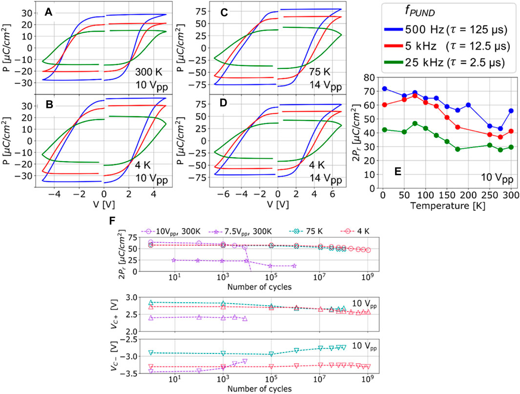
Figure 10. (A, B) P-V characteristics of HZO devices at fixed magnitude of 10 Vpp and different frequencies of 500 Hz, 5 kHz and 25 kHz at 300 K and 4 K. (C, D) P-V characteristics with the critical pulse amplitudes (close to breakdown) of 14 Vpp at different frequencies at 75 K and 4 K. 2Pr as high as 150 µCcm−2 was measured at 4 K and 75 K. (E) 2Pr as a function of temperature T at 10 Vpp and different frequencies. (F) (Top) The polarization as a function of cycling with 10 Vpp at 100 kHz at 500 Hz frequency for 300 K, 75 K, and 4 K (circles). Additionally, 300 K data for 7.5 Vpp measured using the same frequency. (Bottom) The evolution of Vc+ and Vc-as function of switching cycles for different temperatures. Adapted from Bohuslavskyi 2024.
Reproducible analog performance remained a challenge
As discussed in the previous sections, different scientific demonstrations so far confirmed that using mixed polarity of ferroic ordering in spintronic and ferroelectric devices, it is possible to have multiple analog conductance states (Mulaosmanovic, 2015). However, reproducibility and retention of these states remained a challenge, mainly in scaled components (Majumdar, 2019a; Covi, 2022). Recent results from indium–tungsten–oxide (Arabar, 2022) and 2D-semiconductor MoS2 based FeFETs (Majumdar, 2023) demonstrated that with the help of a hybrid FE-dielectric barrier, it is possible to have more controllable analog states. Multiple conductance states obtained from these devices with significantly low read noise and linear and symmetric conductance update under continuously increasing pulse magnitude ensured multi-layer perceptron based deep neural network (DNN) training task can be performed using such FeFETs (Jerry, 2017; Arabar, 2022; Majumdar, 2023). It is found that a significant dispersion in ΔG, the change in synaptic conductance due to subsequent pulses (C2C variation), does not affect training on smaller network (8 × 8 MNIST handwritten dataset) but has detrimental effects with increasing network size. (28 × 28 MNIST handwritten dataset). (Majumdar, 2022b).
Stochasticity in switching is a general feature in nanoscale memristive elements (Tuma, 2016; Mulaosmanovic, 2018). While such stochastic switching is undesirable for precision computing, it can bring certain advantages (McDonnell, 2011; Mass, 2014) for replicating biological computing functions (Faisal, 2008). One such example is probabilistic computing that performs computation upon the probability of a “1” or a “0” state (Li, 2021). Such “1” or “0” can be defined by setting a certain threshold value. For filamentary switching devices, this randomness appears from uncertainty of formation and rupture of filaments while in phase-change memories, such stochasticity results in controlling the phase ratio between the amorphous and crystalline phases (Tuma, 2016). In ferroic components, such uncertainties are due to switching probabilities of FM or FE domains (Atkinson, 2003; Deng, 2020). Generally, a programming voltage of magnitude larger than coercive field value or a pulse width of millisecond or hundreds of microsecond range leads to higher probability of switching compared to sub-threshold pulse amplitude and width. In micron-scale devices, cumulative effect switching from multiple domains makes the randomness in switching much less pronounced compared to ultra-scaled devices where presence of only a few domains makes the switching more probabilistic than deterministic (Mulaosmanovic, 2018). Stochastic switching of nanodevices can be used both in synaptic devices and nano-scale neurons where the randomness in device switching can lead to probabilistic weight distribution in synapses or stochastically firing neurons, mimicking biology more realistically. Current advancement in neuroscience shows that noise, including stochastic resonance, has beneficial effects in specific cases of sensory data processing that forces the neural networks to be more robust and explore more states. The biological neural noise (Faisal, 2008]) is found beneficial to information processing especially in nonlinear systems (McDonnell, 2011) and is essential for computation and learning in cortical microcircuits (Maass, 2014). It is shown that a network built of probabilistic stochastic resonance model of (SRM) neurons under a simple STDP learning rule could be seen as Bayesian computation (Nessler, 2013). Such neural networks can perform probabilistic sampling, inference, and learning algorithms (Buesing, 2011; Pecevski, 2011; Kappel, 2014) and serve as building blocks for biologically plausible implementations of Boltzmann machines (Pedroni, 2013)] and deep belief networks (OConnor, 2013). It has been discussed in different works that nanoscale memristor based probabilistic spiking neurons (Tuma, 2016; Mehonic, 2020; Woo, 2022) can provide potential advantages over their conventional deterministic counterparts, like leaky integrate-and-fire, in implementing flexible learning rules. One such example being the 2D material based memristive Bayesian learning where generalization is done by sampling over a parameter space which provides a certain quantification over the uncertainty, allowing the neural networks to be more robust and explore more states that can be beneficial in specific cases of sensory data processing (Sebastian, 2022).
To conclude, it is important to mention that stochasticity that arises due to inherent abruptness of physical mechanisms in nanoscale devices, like cycle-to-cycle (C2C) and device to device (D2D) variation can be quantified by physics-based modelling (Deng, 2020), and such stochasticity could be already predicted and the circuit and system designers can take appropriate measures to handle those uncertainties. However, batch to batch variation arising from nanotechnology side, i.e., change in device properties due to unintentionally modified fabrication process parameters, for instance, non-uniform metal line edges, any unpredicted contamination issues leading to non-uniform properties and trap distributions, variation in performance due to non-uniformity of growth, thermal processing of thin semiconductor, metal, dielectric or ferroelectric thin films due to non-uniform thermal profile, plasma flow direction and so on that cannot be predicted and modelled beforehand, could lead to unforeseen challenges that the computing circuit is unable to handle.
Depending on the needs for the system to perform on-line training or inference tasks, requirements from the synaptic weight elements vary. For inference tasks, pretrained weights, optimized in software, are transferred to the hardware based on which the system performs classification task on unknown data. Therefore, long-term retention of the synaptic weights is of vital importance (Majumdar, 2022a). However, for on-line training, devices require to optimize the correct synaptic weights by trial and error, drawing conclusions based on the nearest match and eventually correcting the error after several rounds of adjustments on the weights. This requires devices to adjust continuously to new weight values and therefore to have high endurance and reproducibility. Therefore, based on higher retention or endurance of the synaptic weight elements, different application cases can be achieved.
Large-scale integration of neuromorphic and hybrid CMOS–memristor circuits
For a functional circuit, large scale integration of memristor elements is essential. Especially memristors capable of storing analog synaptic weights could implement very compact models of synapses. Multiple layers of vertical stacking of HZO based FTJs (Chen, 2018) and Fe-diodes (Luo, 2020) has been shown utilizing innovative lithography solutions. HZO based FTJs stacked in 2 vertical layers and HZO diodes stacked in 8 vertical layers provided a promising pathway towards ultra-dense implementation of synaptic weight elements. In a hybrid CMOS-memristor circuit approach for mapping the neural network in hardware, two-terminal memristors are integrated in large and dense crossbar arrays (Cai, 2019; Rao, 2023). CMOS neurons together with the memristor crossbars can perform the vector-matrix-multiplication (VMM) in a parallel way and is able to implement neural network training and inference tasks in a fast and energy-efficient manner (Jerry, 2017). The hybrid CMOS - memristor neuromorphic synapse circuits can obtain dense integration of low-power, programmable synaptic weight storage elements and can emulate detailed synaptic dynamics for implementing relevant computational properties of neural systems. The non-linear activation function and temporal dynamics in such systems are implemented by the CMOS circuits, (as shown in Indiveri, 2013). When a CMOS spiking neuron is operated in linear regime, it can time multiplex the contributions from all spiking inputs, thus requiring one single integrating element, saving circuit complexity and cost. However, one significant challenge identified with the RRAM memristor elements being their high degree of performance variability in terms of switching voltage, On/Off currents, getting stuck at one state etc. compared to CMOS synapses. These unreliable and stochastic features become even more prominent as memristors are scaled down (Mulaosmanovic, 2018) and pose serious limitations for high-precision computing. Computing based on hybrid CMOS-FE systems in hardware have not been demonstrated convincingly yet but recent reports from other memristor technologies (Cai, 2019; Rao, 2023) suggest that taking advantage of matured CMOS transistor performance, many shortcomings of the emerging memristive devices can be complemented.
In a regular MRAM based In-memory-computing (IMC) design scheme, connection between the junctions is realized with the CMOS circuits in a crossbar array configuration (Figure 11). Computing with spintronic memristors in an artificial neural network with spintronic synapses have been demonstrated by Borders et al. (Borders, 2016) In this circuit an AFM–FM SOT memristors were used to implement the Hopfield model (Hopfield, 1982), doing patterns association and memorizing. Pattern association was demonstrated (Borders, 2016) using three kinds of 3 × 3 block patterns. The Hopfield network consisting of 36 SOT-based memristors used a field-programmable gate array (FPGA) as neurons. that was controlled by a software running on a computer.
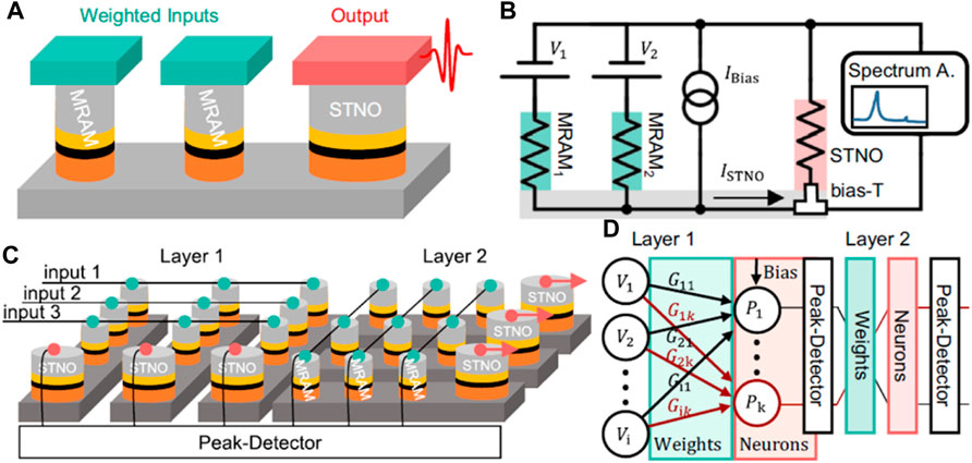
Figure 11. Schematic representation of an MRAM based weighted spin torque nano-oscillators (WSTNO). (A) WSTNO consists of two MRAM memories as weights and a larger nanopillar as an STNO. The MRAMs work as non-volatile weight elements and the STNO work to transfer non-linear function of the neuron. (B) Schematic of the equivalent circuit of the demonstrated system. The input voltages, V1 and V2 are multiplied by the MRAM conductance and used to excite the STNO. The STNO current is converted non-linearly into an oscillating output power. (C, D) Schematics of two layers with 3 inputs and 3 outputs each demonstrating the scaling of the suggested neuromorphic circuit consisting of a crossbar array of MRAMs and STNOs at the output of each layer. The number of inputs, outputs and layers can be scaled, increasing the footprint linearly. Reproduced with permission from Böhnert 2023.
The system was initialized by calculating the ideal synaptic weights based on the Hopfield model for the three chosen patterns are then applied to the synaptic devices. Lack of sufficient linearity and uniformity of the spintronic memristors resulted in 20 iterations for the network to remember the given patterns, however, this work demonstrates that learning with spintronic synapses is possible supported by conventional electronics. This work demonstrated that device non-ideality of spintronic synapses can initially lead to lower classification accuracy, however, high endurance could lead to neuromorphic hardware that can provide superior adaptivity through learning. A CMOS–spintronic circuit was demonstrated by Marković et al. (Marković, 2020) that showed a system with 128 inputs and 128 outputs consumes 23 nJ per operation for learning that eventually reduces to 7.4 nJ post-learning. This is a promising improvement over 330 nJ per operation for a low-power spiking CMOS neurons-based system. Hybrid CMOS-spintronics spiking neural network has been demonstrated by Sengupta et al. with on-chip learning capabilities (Sengupta, 2016a).
Other than conventional CMOS-MRAM systems, computation can be done using the device physics. It has been shown that using the domain wall motion, an all-spin ANN system can be designed (Sengupta, 2016b) while using dipolar coupling between nanomagnets, it is possible to directly do computation based on energy minimization that can reduce the CMOS circuit overhead. Physical dipolar interaction between arrays of nanomagnets were used by Bhanja et al. (Bhanja, 2016) to solve a quadratic optimization problem for computer vision applications. A reservoir computing system was demonstrated with dipole-coupled nanomagnets by Nomura et al. (Nomura, 2019) The future of this field is extremely promising with the prospect of utilizing the natural physics of nanomagnets for implementing ultralow-power, scaled ANNs. Also, classification of signals at microwave frequencies was demonstrated by Romera et al. (Romera, 2018) in a small, two-layer neural network by computing with synchronized spin-torque nano-oscillators, providing a promising way for high-frequency signal processing.
For integrating devices into a functional circuit one key consideration is connectivity. In a typical neural network algorithm today, 10 to 1,000 synapses per neuron are used, in comparison to the 10,000 synapses per neuron in the human cerebral cortex. Therefore, the biggest challenge of mimicking biology in neuromorphic hardware is to attain dense interconnection between neurons. Interconnect technology is an extensive research subject that is bringing in improved solutions every day (Wesling, 2020). Spintronic and ferroelectric systems, especially the MTJs and FTJs are made of trilayer systems that can be vertically stacked making it in possible to have dense integration possible in three dimensions. However, while considering such 3D vertical integration, interconnection between layers is a critical consideration. In spintronic nanostructures, vertical and horizontal communication through optical waves or microwave signals emitted by STNOs, could be useful. However, in such cases, an amplifier circuit might be essential to achieve high fan-out. Progress in ferroic materials and device technologies are expected to bring promising possibilities for building complex 3D-integrated computing hardware.
Computing with ferroelectric memristors
As discussed previously, partial rotation of ferroelectric domains results in multiple conductance states in FeFETs and in literature it has been shown that proper control of these intermediate states via gate stack modification (Majumdar, 2023) or a custom-designed programming pulse protocols (Jerry, 2017) can lead to quite linear and symmetric weight update. Efficient DNN training has been demonstrated utilizing the analog synaptic weight update in FeFET-based synapses where proper dynamics of partial polarization switching were induced by the gate voltage-controlled channel conductance (Jerry, 2017; De, 2022; Majumdar, 2023). Figure 12C shows schematically how FeFET based analog crossbar array can perform VMM operation. In the crossbar array, each cross point between row and columns represents one FeFET transistor. This array, surrounded by neuron circuitry, implement the training algorithm i.e., the forward propagation, back propagation, and weight-update operations. In these circuits higher parallelism is achieved using neuron circuit at each row and column that can bypass time-multiplexing. For a compact hardware implementation of such hybrid CMOS-FeFET neural network, FeFETs could be either integrated with CMOS at front end of line (FEOL) or back end of line (BEOL). Co-integration of FeFETs into standard high-k metal gate (HKMG) CMOS platforms were demonstrated by Beyer et al. (Beyer, 2020), leading to a cheap, fast, low-power eFLASH replacement for existing eNVM technology nodes. The FeFETs showed a reversible switching between a low-VT (LVT) and a high-VT (HVT) state with a MW of 1.5 V and a good uniformity. A linear increase in programming or erasing voltage led to an exponential increase in the switching speed and found to be independent of the device size, i.e., also observable for ultra-scaled FeFETs (Mulaosmanovic, 2018). The switching time vs VG curves were found highly sensitive to fabrication process variations and found to shift with respect to the VG axis or change the slope, leading to short- and long-term retention trends (Mulaosmanovic, 2017). From a system level perspective, Berdan et al. demonstrated FTJ crossbars can scale analogue VMM-intensive applications, like neural inference engines leading towards energy efficiencies above 100 tera-operations per second per watt (Berdan, 2020). while utilizing both volatile and nonvolatile retention of ferroelectric diodes, Chen et al. showed all-ferroelectric reservoir computing systems can be achieved that can operate as a reliable and low-power neuromorphic hardware for temporal information processing (Chen, 2023).
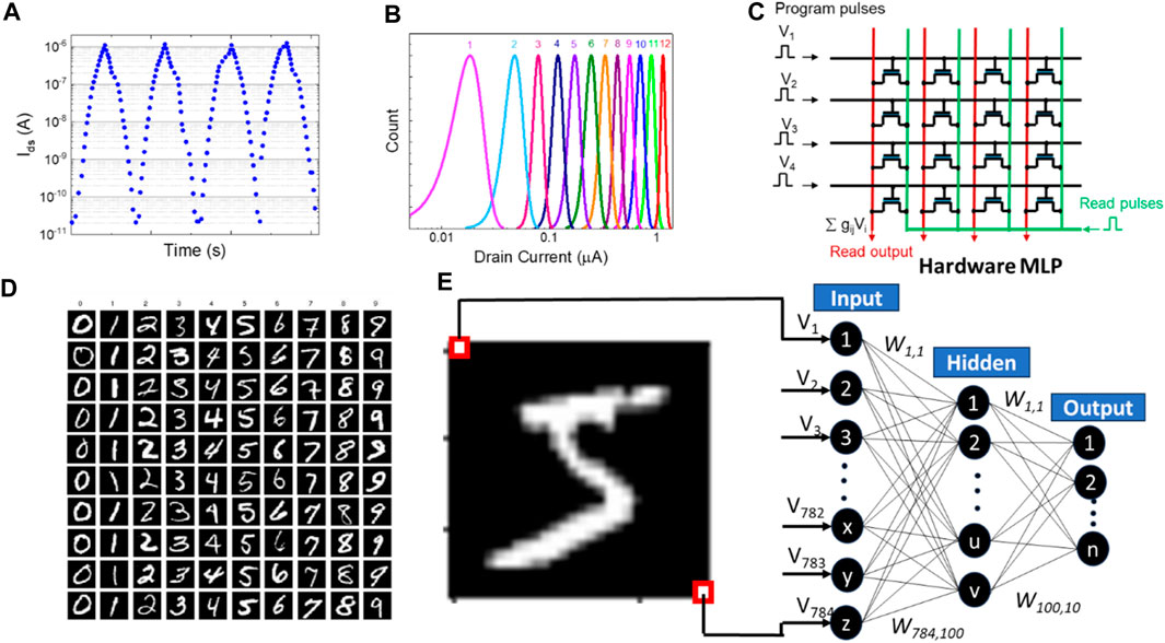
Figure 12. (A) Channel currents in analog FeFET device over multiple pulsed switching cycles showing reproducible intermediate state switching. (B) Distribution of the 12 conductance states of the FeFET device over multiple cycles of weight update. (C) Schematic diagram of the vector matrix multiplication (VMM) architecture using FeFET based crossbar arrays where programming voltage pulses are used as input to the rows connecting the gate terminals and current outputs are extracted from the columns connecting the drain current terminals. The synaptic weight is indicated by the conductance of each FeFET (gij). The current output from the crossbar is the product of the input voltage (Vi) and FeFET channel conductance (gij). (D–E) Schematic illustration of MNIST handwritten dataset (D) and its classification operation in a multi-layer perceptron based deep neural network.
Integration technologies–features and challenges
All non-volatile memory and synaptic or neuronal devices need to be eventually integrated into a complete system, and therefore combining the memory and synaptic circuits with CMOS-based technologies, are essential. This brings about a whole set of integration challenges. There have been efforts to integrate different components using standard techniques (Heterogeneous integration Roadmap, 2023 edition, Emerging Research Devices), such as 2D, 2.5D and 3D integration of devices with silicon transistors either in the same plane or vertically stacked on top of each other.
2D planar and 2.5D integration are comparatively matured technologies (Sheikh, 2021). In 2D techniques, simple in-plane interconnects are used while 2.5D integration uses silicon interposer techniques, where a chip with lithographically defined interconnections and through-silicon via’s (TSV) communicate between different functional units (Gambino, 2015). Although matured, efforts are still needed to reduce the pitch, incorporating large numbers of connections for routing signals between different functional components and loss through interconnects for large-scale integration of neuromorphic circuits. Optimization of materials, etching chemistry and layouts are therefore of vital importance (Rofeh, 2015). In 3D monolithic integration, memory components are grown directly on top of the CMOS wafer and therefore managing the thermal budget is an important issue (Yu, 2021). Although 3D integration can provide highest integration density and low loss interconnects, it imposes material challenges due to the direct growth technique leading to material compatibility issues.
Depending on the application, therefore it is important to choose the correct integration technology. Systems where thermally evaporated magnetic metals or low thermal budget ferroelectric materials can serve the purpose, can use 3D technologies while applications demanding more exotic functionalities need to depend on heterogeneous 2D or 2.5 D integration. Need for high memory bandwidth, less operational heat dissipation, better mechanical stability, and affordable cost would define the technology for building the next-generation neuromorphic systems. In the following section, we discuss a few implemented integration methodologies and their advantages and challenges.
Heterogeneous integration: Heterogeneous integration, where systems on chip and in package can be realized by combining spintronics–CMOS or ferroelectric–CMOS and other components developed on different substrates, makes it possible to integrate exotic material properties of complex oxide material classes. For spintronic systems, complex-oxide materials exhibit a wide range of exotic, functional properties (Majumdar, 2013). However, due to their demanding and non-CMOS compatible fab conditions and requirements for special substrates make them unsuitable for direct integration with CMOS logic and other functional circuits. In such cases, heterogeneous integration and application of strain through heteroepitaxy provide an attractive choice, that can make integration of complex oxides possible with mature semiconductor technologies. Kum et al. demonstrated a universal mechanical exfoliation method (Kum, 2020) that can produce freestanding single-crystalline membranes of complex-oxide materials including perovskite, spinel and garnet crystal structures that can be stacked directly with CMOS electronics, similar to two-dimensional material-based heterostructures, and an integrated logic-memory or neuron synaptic architectures can be realized.
3D Monolithic integration: As mentioned previously, advantages of 3D integration include i) reduced interconnect wire length resulting in lower delay and power, ii) lower parasitic effects, iii) higher packaging density and lower footprint. However, 3D monolithic integration comes at a cost of limited design space for materials and process parameters. Since, devices and circuits are formed in the back-end-of-line of CMOS circuits, no process fabrication steps can exceed a temperature of 500°C and long-term thermal exposure or exposure to chemicals that can affect the passivation layers. In terms of ferromagnetic and ferroelectric materials, this limits the material choice to either evaporated or sputtered transition metals like Fe, Co, Ni and alloys for spintronics and mainly ALD-grown hafnia-based systems for ferroelectric devices. Since 3D monolithic integration technology is a rather recent trend in semiconductor industry, not too much study has been done on 3D integrated spintronic and ferroelectric systems and therefore fabrication and performance limitations are not yet so well understood. Small-scale integrations have been reported for ferroelectric hafnia-based capacitors and FETs (Francois, 2019; Dutta 2020; De, 2022), mainly showing moderate sized memory arrays or mainly CMOS compatible process for FeFETs and SOT-MRAMs respectively (Garello, 2018; Falcone, 2022). Future studies need to advance the knowledge of performance reliability and limitations in such systems and needs for custom materials designs to improve functionalities in such systems.
Application in neuromorphic computing tasks
Deep-Learning Accelerators: High complexity AI tasks, such as image classifications or natural language processing require running of large DNN models with multiple hidden layers. Hardware implementation of such DNN models would benefit massively from high-degree of parallelism obtained by In-memory computing taking place in large crossbar arrays of memristors that map the weight metrices. In IMC primitive, higher prediction accuracy for the AI algorithm model parameters demands higher bit resolution of synaptic weights compared to the highest possible bits per cell in synaptic devices (Jerry, 2017; Luo, 2022). To address such challenges, one possible way is to map the input vectors and weight matrices into multiple crossbar arrays or columns (Wang, 2021). However, determining the system-level efficiency would require considerations from peripheral circuit components, handling the data from to and from the crossbars as well. For instance, in a hardware neural network, the bits of input vector are converted to voltages, and streamed to the synaptic array. Timing of the streaming depends on the bit-precision of the digital-analog converters (DAC). After the voltage pulses pass through the synapses, the dot product of the input voltage vector and conductance matrix is accumulated as current from the columns of crossbar. The output currents are processed in combination with results from multiple time steps or multiple arrays in bit streaming or bit slicing scheme to perform multi-bit VMM operations. The output currents from one or multiple crossbars pass through analog-digital converters (ADC) to get the final output. Multi-level synaptic devices help mapping the synaptic weights onto the crossbar more efficiently, however it increases requirement for bit precision of the ADC making it most power and area consuming element in the circuit. While devices with multiple levels can decrease the number of synaptic weight elements or number of crossbar arrays in the circuit, higher power and area consumption of ADCs need to be considered while estimating the circuit implementation. Fewer bits per cell synapses, on the other hand, need multiple cross bars to implement the weight mapping. However, the lower bit precision requirement in the ADCs makes the power an area footprint lower for the ADCs. Based on the application, a correct trade off, therefore, needs to be found out and design optimization needs to be done. So far, most of the reported results on IMC hardware predicted the system-level performance based on individual device measurements extrapolated to system level simulation. (Dutta 2020; Bégon-Lours, 2021). However, in these cases, device to device variation, effect of parasitics, size of the crossbar, number of failed or stuck devices have not been taken into account. In future works, full hardware implementation of the crossbar-based computation needs to be done and systematic co-optimization at the material, device, circuit and systems level performed to achieve best results. Some recent works on large-scale integration of CMOS-RRAM systems (Cai, 2019) or CMOS-STT-MRAM systems (Lee, 2019) can provide roadmap in this direction.
Spiking-Neural Network: In comparison to the DNNs, SNNs are more versatile in handling the spatio-temporally varying signal encoding and processing. In SNNs, neurons communicate with each other using binary signals or spikes and timing of the spikes encodes the data. Accumulative and threshold switching behaviour of ferroic devices can make them extremely efficient for hardware implementation of SNNs, both as synaptic weight elements and as leaky-integrate and fire neurons. Utilizing memristive synapses as weight elements, both supervised training and unsupervised training and adaptation has been demonstrated. The unsupervised learning, where the synaptic weights are modified in an unsupervised manner according to the biologically inspired STDP rule (Poo 1998), is rather straightforward to implement in hardware. The STDP rule implements the experimental observation that when a synapse is subjected to a pre-pulse before a post-pulse, the effective synaptic strength increases, and if the pulse ordering reverses, it results in an effective decrease in synaptic strength. Shape and duration of the input pulses can impact the change of synaptic conductance (Majumdar, 2019a). Utilizing hybrid CMOS-Memristor circuits IBM researchers demonstrated an integrated neuromorphic core with 256 × 256PCM synapses fabricated together with CMOS neurons that is capable of on-chip learning based on a simplified STDP rule and can perform auto-associative pattern learning tasks (Kim, 2015). Fang et al. demonstrated that certain optimization problems could be solved efficiently utilizing the coupled dynamics of FeFET-based spiking neurons. It was shown that coupled neurons, with 1T-FeFET structures showing both excitory and inhibitory inputs, communicate and modulate each other’s action potentials through event-driven spikes and synchronize their dynamics around the states of optimal solutions (Fang, 2019).
In comparison to the unsupervised learning, implementing a supervised learning in SNN is a more demanding task due to the inherent difficulty in applying gradient descent methods for spiking neuron models with infinite discontinuities at the instants of spikes (Mehonic, 2020). Although, there has been some demonstrations (Nandakumar 2017), there is still urgent needs for development of robust and event-driven learning algorithms for SNNs.
Considering the randomness of the memristive synaptic devices, Bayesian inference and learning could be one potentially important strategy for memristive neural networks in general. Unlike the conventional approach where a single set of parameter vector is used during learning, the Bayesian principle utilises the inference over a probability distribution of the synaptic weights. In presence of sufficient data this distribution focuses on the optimal weight configuration, however, when data are limited, the synaptic weight distribution provides a so-called credibility profile in the parameter space, enabling most probable solutions during inference and exploration during learning.
For applications down to deep cryogenic temperatures, specific features and limitations of both memristive and cryo-CMOS components need to be studied and modelled carefully.
Challenges and future perspectives
The discussion so far highlighted many aspects of ferroic devices that can bring substantial advantages in achieving neuromorphic computing hardware, especially suitable for operation down to cryogenic temperatures. Briefly summarizing, the biggest advantages of devices with ferroic ordering being, 1) non-volatility, i.e., spintronic and ferroelectric analog memories can possess long term data retention making them suitable for applications where data persistence is crucial, such as in embedded systems and IoT devices and for AI-inference tasks. 2) Low Power Consumption in comparison to traditional memory technologies like DRAM or flash, spintronic and ferroelectric analog memories can offer lower power consumption making them attractive for battery-powered devices and energy-efficient computing. 3) High Speed: Spintronic and ferroelectric polarization switching being extremely fast, the ferroic devices can operate at high speeds, making them suitable for applications that require rapid data access and processing, such as real-time signal processing and machine learning accelerators. 4) Endurance: Spintronic and ferroelectric memories often have excellent endurance, with the potential for a high number of write and erase cycles without significant degradation or fatigue effects. This endurance is advantageous for applications that require frequent data updates like synaptic devices where online training operation is needed in a neural network accelerator. 5) Integration with CMOS: Spintronic and ferroelectric devices can be integrated with CMOS technology, allowing for the development of hybrid memory and logic circuits on a single chip. This integration can lead to more compact and efficient systems. 6) Resistance to Radiation: Spintronic and ferroelectric devices are inherently less susceptible to radiation-induced errors compared to some other memory technologies, making them suitable for space and high-radiation environments.
However, some material, fabrication and performance challenges still exist that require substantial research efforts in this direction. 1) Material Complexity: Spintronic and ferroelectric memories rely on specialized materials, electrodes and design principles to operate efficiently as analog memories. The fabrication of these materials and devices can be complex and costly. 2) Write Currents: Writing data in spintronic memories typically involves passing a significant current through the MTJs, which can lead to high power consumption and heat generation. Developing low power write schemes is a challenge in spintronic components while in FTJs, the challenge is opposite. In scaled FTJs, the read current is often too low to avoid read noise and successfully read the programmed states. 3) Retention and Data Stability: The stability of stored data in spintronic and ferroelectric memories, especially in high-temperature environments and for multiple analog states, is a concern. Ensuring long-term data retention without degradation is essential for non-volatile retention purpose. However, for synaptic weight elements, non-volatile retention time scale can be different and might not pose challenges. 4) Manufacturability and Yield: Scaling up the production of spintronic and ferroelectric memories and achieving >95% yields can be challenging due to the intricacies of material deposition and device fabrication. 5) Variability: Variability in material properties and manufacturing processes can lead to significant performance variations between individual devices. Achieving uniformity and reliability is crucial for mass adoption of these technologies. 6) Cost: The cost of manufacturing spintronic memories, particularly in comparison to established memory technologies like NAND flash or DRAM, can be a barrier to widespread adoption. Reducing production costs is a significant challenge. 6) Compatibility: Integrating spintronic memories with existing electronics and semiconductor processes may require adaptations and standards. Compatibility with current computing architectures and interfaces is important for adoption. 7) Error Correction: Like other memory technologies, spintronic memories may require advanced error correction techniques to maintain data integrity, particularly as they are used in more demanding applications.
To summarize, spintronic and ferroelectric analog memories offer a range of advantages, including non-volatility, low power consumption, almost infinite endurance, and high speed. However, they face challenges related to materials, manufacturability, variability affecting analog data stability, and cost. Researchers and engineers are actively working to overcome these challenges and unlock the full potential of spintronic and ferroelectric memories in various applications, including embedded systems, IoT, and high-performance computing. Merged logic-memory systems or neuromorphic architectures require a holistic design approach where different cross-layer design, optimization and implementation is needed to create a scalable, high-performance, and energy-efficient chip that is based on materials physics and critical nanotechnology. When successfully scaled, these proposed computation platforms will be able to provide 1,000× improvement in computing performance in terms of energy-latency product. This will be particularly efficient for memory-intensive computing tasks like real-time recognition of images and videos, on-line learning, big-data analytics, secure computing etc. Future research from hardware side should focus on large-scale integration of on-chip memory with energy-efficient computation circuits. Innovations around monolithic 3D integration technologies will be able to provide ultra-high connectivity improving the system level performance while reducing power loss, delay and cost. From circuit, systems and applications side, innovations are needed for computing architectures that embrace sparsity, stochasticity, and nanodevice variability, mimicking human brain. While today’s artificial neural networks are supporting large-scale machine learning applications on the cloud, computing hardware supporting these cognitive systems suffer from long and power intensive training times, large training datasets, lack of flexibility and dynamic adaptation, and real-time autonomous decision-making. By leveraging innovations in novel materials and device technologies to create merged logic-memory fabrics, it is possible to accelerate development of real time operating cognitive and secure computing systems.
Different computational models like compute-in-memory, reinforcement learning, hyper-dimensional computing, approximate computing, spike-based computing and so on are used to demonstrate the cognitive ability of the hardware. Utilizing the physics of the novel devices it is possible to overcome the current limitations and achieve dynamic adaptation and parallel on-line learning. Innovations in integration technologies will ensure large-scale systems, capable of handling real world complex problems enabling ubiquitous intelligent systems under energy constrained situations.
Finally, we envision that the development of neuromorphic hardware would require extensive efforts and cross-disciplinary knowledge from different communities, from neuroscience to physics, materials science, nanotechnology, electrical and computer engineering and collaborative efforts could lead to successful development of achievement of the next-generation of energy-efficient, secure and cognitive integrated microsystems. Photo-induced magnetoresistance (Elovaara, 2015) or ferroelectric effects (Tan, 2022) can pave the way for photonic memory and neuromorphic circuits based on ferroic devices. The current review provided an outlook on the designing of energy-efficient, analog memories, synaptic weight and neuronal elements utilizing the physics of ferromagnetic or ferroelectric materials, that could provide multiple benefits for large range of applications with special focus on cryogenic applications for quantum computing and space technologies.
Author contributions
SM: Conceptualization, Funding acquisition, Project administration, Writing–original draft, Writing–review and editing.
Funding
The author(s) declare that no financial support was received for the research, authorship, and/or publication of this article.
Acknowledgments
The author acknowledges financial support from Research Council of Finland through projects AI4AI (no. 350667) and FerrARI (no. 359047) and Business Finland and European Commission through project ArCTIC (no. 101139908).
Conflict of interest
The author declares that the research was conducted in the absence of any commercial or financial relationships that could be construed as a potential conflict of interest.
Publisher’s note
All claims expressed in this article are solely those of the authors and do not necessarily represent those of their affiliated organizations, or those of the publisher, the editors and the reviewers. Any product that may be evaluated in this article, or claim that may be made by its manufacturer, is not guaranteed or endorsed by the publisher.
References
Aabrar, K. A., Kirtania, S. G., Liang, F.-X., Gomez, J., Jose, M. S., Luo, Y., et al. (2022). BEOL-compatible superlattice FEFET analog synapse with improved linearity and symmetry of weight update. IEEE Trans. Electron Devices 69, 2094–2100. doi:10.1109/ted.2022.3142239
Angervo, I., Saloaro, M., Palonen, H., Huhtinen, H., Paturi, P., Mäkelä, T., et al. (2022). Giant magnetoresistance response in Sr2FeMoO6 based organic spin valves. Appl. Surf. Sci. 589, 152854. doi:10.1016/j.apsusc.2022.152854
Atkinson, D., Allwood, D. A., Xiong, G., Cooke, M. D., Faulkner, C. C., and Cowburn, R. P. (2003). Magnetic domain-wall dynamics in a submicrometre ferromagnetic structure. Nat. Mater 2, 85–87. doi:10.1038/nmat803
Bégon-Lours, L., Halter, M., Popoff, Y., and Offrein, B. J. (2021). Special issue:emerging fluorite- and wurtzite-type ferroelectrics. Phys. Stat. Solidi RRL 15, 2000524. doi:10.1002/pssr.202000524
Berdan, R., Marukame, T., Ota, K., Yamaguchi, M., Saitoh, M., Fujii, S., et al. (2020). Low-power linear computation using nonlinear ferroelectric tunnel junction memristors. Nat. Electron. 3, 259–266. doi:10.1038/s41928-020-0405-0
Berger, L. (1996). Emission of spin waves by a magnetic multilayer traversed by a current. Phys. Rev. B 54, 9353–9358. doi:10.1103/physrevb.54.9353
Beyer, S., Dunkel, S., Trentzsch, M., Muller, J., Hellmich, A., Utess, D., et al. (2020). “FeFET: a versatile CMOS compatible device with game-changing potential,” in 2020 IEEE International Memory Workshop (IMW), Dresden, Germany, 17-20 May 2020, 1–4.
Bhanja, S., Karunaratne, D. K., Panchumarthy, R., Rajaram, S., and Sarkar, S. (2016). Non-Boolean computing with nanomagnets for computer vision applications. Nat. Nanotechnol. 11, 177–183. doi:10.1038/nnano.2015.245
Böhnert, T., Rezaeiyan, Y., Claro, M. S., Benetti, L., Jenkins, A. S., Farkhani, H., et al. (2023). Weighted spin torque nano-oscillator system for neuromorphic computing. Commun. Eng. 2, 65. doi:10.1038/s44172-023-00117-9
Bohuslavskyi, H., Griogoras, K., Ribeiro, M., Prunnila, M., and Majumdar, S. (2024). Ferroelectric Hf0.5Zr0.5O2 for analog memory and in-memory computing applications down to deep cryogenic temperatures. Adv. Elec. Mater. doi:10.1002/aelm.202300879
Borders, W. A., Akima, H., Fukami, S., Moriya, S., Kurihara, S., Horio, Y., et al. (2016). Analogue spin–orbit torque device for artificial neural-network-based associative memory operation. Appl. Phys. Express 10, 013007. doi:10.7567/apex.10.013007
Boyn, S., Grollier, J., Lecerf, G., Xu, B., Locatelli, N., Fusil, S., et al. (2017). Learning through ferroelectric domain dynamics in solid-state synapses. Nat. Commun. 8, 14736. doi:10.1038/ncomms14736
Buesing, L., Bill, J., Nessler, B., and Maass, W. (2011). Neural dynamics as sampling: a model for stochastic computation in recurrent networks of spiking neurons. PLoS Comput. Biol. 7 (11), e1002211. doi:10.1371/journal.pcbi.1002211
Cai, F., Correll, J. M., Lee, S. H., Lim, Y., Bothra, V., Zhang, Z., et al. (2019). A fully integrated reprogrammable memristor–CMOS system for efficient multiply–accumulate operations. Nat. Electron. 2 (7), 290–299. doi:10.1038/s41928-019-0270-x
Chanthbouala, A., Matsumoto, R., Grollier, J., Cros, V., Anane, A., Fert, A., et al. (2011). Vertical-current-induced domain-wall motion in MgO-based magnetic tunnel junctions with low current densities. Nat. Phys. 7, 626–630. doi:10.1038/nphys1968
Chen, A. (2022). Beyond-CMOS roadmap—from Boolean logic to neuro-inspired computing. Jpn. J. Appl. Phys. 61, SM1003. doi:10.35848/1347-4065/ac5d86
Chen, L., Wang, T. Y., Dai, Y. W., Cha, M. Y., Zhu, H., Sun, Q. Q., et al. (2018). Ultra-low power Hf0.5Zr0.5O2 based ferroelectric tunnel junction synapses for hardware neural network applications. Nanoscale 10, 15826–15833. doi:10.1039/c8nr04734k
Chen, Z., Li, W., Fan, Z., Dong, S., Chen, Y., Qin, M., et al. (2023). All-ferroelectric implementation of reservoir computing. Nat. Commun. 14, 3585. doi:10.1038/s41467-023-39371-y
Covi, E., Mulaosmanovic, H., Max, B., Slesazeck, S., and Mikolajick, T. (2022). Ferroelectric-based synapses and neurons for neuromorphic computing. Neuromorph. Comput. Eng. 2, 012002. doi:10.1088/2634-4386/ac4918
Dahlberg, H., and Wernersson, L.-E. (2023). “Dynamics of polarization switching in mixed phase ferroelectric-antiferroelectric HZO thin films,” in ESSDERC 2023 - IEEE 53rd European Solid-State Device Research Conference (ESSDERC), Lisbon, Portugal, 11-14 September 2023, 33–36.
De, S., Le, H. H., Qiu, B. H., Baig, M. A., Sung, P. J., Su, C. J., et al. (2021a). Robust binary neural network operation from 233 K to 398 K via gate stack and bias optimization of ferroelectric FinFET synapses. IEEE Electron Device Lett. 42 (8), 1144–1147. doi:10.1109/LED.2021.3089621
De, S., Muller, F., Laleni, N., Lederer, M., Raffel, Y., Mojumder, S., et al. (2022). Demonstration of multiply-accumulate operation with 28 nm FeFET crossbar array. IEEE Electron Device Lett. 43 (12), 2081–2084. doi:10.1109/led.2022.3216558
De, S., Qiu, B.-H., Bu, W.-X., Baig, Md. A., Sung, P.-J., Su, C.-J., et al. (2021b). Uniform crystal formation and electrical variability reduction in hafnium-oxide-based ferroelectric memory by thermal engineering. ACS Appl. Electron. Mat. 3 (2), 619–628. doi:10.1021/acsaelm.0c00610
Deng, S., Yin, G., Chakraborty, W., Dutta, S., Datta, S., Li, X., et al. (2020). “A comprehensive model for ferroelectric FET capturing the key behaviors: scalability, variation, stochasticity, and accumulation,” in 2020 IEEE Symposium on VLSI Technology, Honolulu, HI, USA, 16-19 June 2020, 1–2.
Elovaara, T., Majumdar, S., Huhtinen, H., and Paturi, P. (2015). Photoinduced colossal magnetoresistance under substantially reduced magnetic field. Adv. Funct. Mater. 25, 5030–5037. doi:10.1002/adfm.201502233
Endo, M., Kanai, S., Ikeda, S., Matsukura, F., and Ohno, H. (2010). Electric-field effects on thickness dependent magnetic anisotropy of sputtered MgO/Co40Fe40B20/Ta structures. Appl. Phys. Lett. 96, 212503. doi:10.1063/1.3429592
Faisal, A. A., Selen, L. P., and Wolpert, D. M. (2008). Noise in the nervous system. Nat. Rev. Neurosci. 9 (4), 292–303. doi:10.1038/nrn2258
Falcone, F., Halter, M., Bégon-Lours, L., and Offrein, B. J. (2022). Back-end, CMOS-compatible ferroelectric FinFET for synaptic weights. Front. Electron. Mater, Sec. Semicond. Mater. Devices 2, 849879. doi:10.3389/femat.2022.849879
Fang, Y., Wang, Z., Gomez, J., Datta, S., Khan, A. I., and Raychowdhury, A. (2019). A swarm optimization solver based on ferroelectric spiking neural networks. Front. Neurosci. 13, 855. doi:10.3389/fnins.2019.00855
Fernández-Pacheco, A., Streubel, R., Fruchart, O., Hertel, R., Fischer, P., and Cowburn, R. P. (2017). Three-dimensional nanomagnetism. Nat. Commun. 8, 15756. doi:10.1038/ncomms15756
ferroelectric memristor, A., Chanthbouala, A., Garcia, V., Cherifi, R. O., Bouzehouane, K., Fusil, S., et al. (2012). A ferroelectric memristor. Nat. Mater. 11, 860–864. doi:10.1038/nmat3415
Finocchio, G., Ventra, M. D., Camsari, K. Y., Everschor-Sitte, K., Amiri, P. K., and Zeng, Z. (2021). The promise of spintronics for unconventional computing. J. Magn. Magn. Mat. 521 (1), 167506. doi:10.1016/j.jmmm.2020.167506
Francois, T., Grenouillet, L., Coignus, J., Blaise, P., Carabasse, C., Vaxelaire, N., et al. (2019). “IEDM 2019 welcome,” in IEEE International Electron Devices Meeting (IEDM), San Francisco, United States, 7-11 December 2019.
Fukami, S., Anekawa, T., Zhang, C., and Ohno, H. (2016a). A spin–orbit torque switching scheme with collinear magnetic easy axis and current configuration. Nat. Nanotechnol. 11, 621–625. doi:10.1038/nnano.2016.29
Fukami, S., Zhang, C., Dutta Gupta, S., Kurenkov, A., and Ohno, H. (2016b). Magnetization switching by spin-orbit torque in an antiferromagnet-ferromagnet bilayer system. Nat. Mat. 15, 535–541. doi:10.1038/nmat4566
Gambino, J. P., Adderly, S. A., and Knickerbocker, J. U. (2015). An overview of through-silicon-via technology and manufacturing challenges. Microelectron. Eng. 135, 73–106. doi:10.1016/j.mee.2014.10.019
Garcia, V., and Bibes, M. (2014). Ferroelectric tunnel junctions for information storage and processing. Nat. Commun. 5, 4289. doi:10.1038/ncomms5289
Garcia, V., Bibes, M., Barthelemy, A., Bowen, M., Jacquet, E., Contour, J.-P., et al. (2004). Temperature dependence of the interfacial spin polarization of La2/3Sr1/3MnO3. Phys. Rev. B69, 052403. doi:10.1103/PhysRevB.69.052403
Garello, K., Yasin, F., Couet, S., Souriau, L., Swerts, J., Rao, S., et al. (2018). “SOT-MRAM 300MM integration for low power and ultrafast embedded memories,” in 2018 IEEE Symposium on VLSI Circuits, Honolulu, HI, USA, 18-22 June 2018, 81–82.
Goh, Y., Cho, S. H., Park, S.-H. K., and Jeon, S. (2020). Crystalline phase-controlled high-quality hafnia ferroelectric with RuO₂ electrode. IEEE Trans. Electron Devices 67, 3431–3434. doi:10.1109/ted.2020.2998444
Grimaldi, A., Selcuk, K., Aadit, N. A., Kobayashi, K., Cao, Q., Chowdhury, S., et al. (2022). “Experimental evaluation of simulated quantum annealing with MTJ-augmented p-bits,” in 2022 International Electron Devices Meeting (IEDM), San Francisco, CA, USA, December 3-7, 2022, 22.4.1–22.4.4.
Grimaldi, E., Lebrun, R., Jenkins, A., Dussaux, A., Grollier, J., Cros, V., et al. (2014). “Spintronic nano-oscillators: towards nanoscale and tunable frequency devices,” in 2014 IEEE International Frequency Control Symposium (FCS), Taipei, Taiwan, 19-22 May 2014, 1–6.
Grollier, J., Boulenc, P., Cros, V., Hamzić, A., Vaurès, A., Fert, A., et al. (2003). Switching a spin valve back and forth by current-induced domain wall motion. Appl. Phys. Lett. 83, 509–511. doi:10.1063/1.1594841
Grollier, J., Querlioz, D., Camsari, K. Y., Everschor-Sitte, K., Fukami, S., and Stiles, M. D. (2020). Neuromorphic spintronics. Nat. Electron. 3, 360–370. doi:10.1038/s41928-019-0360-9
Gruverman, A., Wu, D., Lu, H., Wang, Y., Jang, H. W., Folkman, C. M., et al. (2009). Tunneling electroresistance effect in ferroelectric tunnel junctions at the nanoscale. Nano Lett. 9, 3539–3543. doi:10.1021/nl901754t
Gupta, A., Gong, G. Q., Xiao, G., Duncombe, P. R., Lecoeur, P., Trouilloud, P., et al. (1996). Grain-boundary effects on the magnetoresistance properties of perovskite manganite films. Phys. Rev. B 54, R15629(R)–R15632. doi:10.1103/physrevb.54.r15629
Hawley, M. E., Brown, G. W., Yashar, P. C., and Kwon, C. (2000). H-dependent magnetic domain structures in La0.67Sr0.33MnO3 thin films. J. Cryst. Growth 211 (1–4), 86–92. doi:10.1016/s0022-0248(99)00849-0
Hayashi, M., Thomas, L., Rettner, C., Moriya, R., Jiang, X., and Parkin, S. S. P. (2006). Dependence of current and field driven depinning of domain walls on their structure and chirality in permalloy nanowires. Phys. Rev. Lett. 97, 207205. doi:10.1103/physrevlett.97.207205
Hayward, T. J. (2015). Intrinsic nature of stochastic domain wall pinning phenomena in magnetic nanowire devices. Sci. Rep. 5, 13279. doi:10.1038/srep13279
Henry, M. D., Smith, S. W., Lewis, R. M., and Ihlefeld, J. F. (2019). Stabilization of ferroelectric phase of Hf0.58Zr0.42O2 on NbN at 4 K. Appl. Phys. Lett. 114, 092903. doi:10.1063/1.5052435
Heterogeneous integration roadmap (2023) Heterogeneous integration roadmap edition. Available at: https://eps.ieee.org/technology/heterogeneous-integration-roadmap/2023-edition.html.
Hopfield, J. J. (1982). Neural networks and physical systems with emergent collective computational abilities. Proc. Natl. Acad. Sci. U. S. A. 79, 2554–2558. doi:10.1073/pnas.79.8.2554
Houshang, A., Iacocca, E., Dürrenfeld, P., Sani, S. R., Åkerman, J., and Dumas, R. K. (2016). Spin-wave-beam driven synchronization of nanocontact spin-torque oscillators. Nat. Nanotechnol. 11, 280–286. doi:10.1038/nnano.2015.280
Hur, J., Luo, Y. C., Wang, Z., Lombardo, S., Khan, A. I., and Yu, S. (2021). Characterizing ferroelectric properties of Hf0.5Zr0.5O2 from deep-cryogenic temperature (4 K) to 400 K. IEEE J. Explor. Solid-State Comput. Devices Circuits 7, 168–174. doi:10.1109/jxcdc.2021.3130783
Hur, J., Park, C., Choe, G., Ravindran, P. V., Khan, A. I., and Yu, S. (2022). Characterizing HfO2-based ferroelectric tunnel junction in cryogenic temperature. IEEE Trans. Electron Devices 69 (10), 5948–5951. doi:10.1109/ted.2022.3200919
Ielmini, D., and Ambrogio, S. (2020). Emerging neuromorphic devices. Nanotechnology 31, 092001. doi:10.1088/1361-6528/ab554b
Ikegawa, S., Mancoff, F. B., Janesky, J., and Aggarwal, S. (2020). Magnetoresistive random access memory: present and future. IEEE Trans. Electron Devices 67 (4), 1407–1419. doi:10.1109/ted.2020.2965403
Indiveri, G., Linares-Barranco, B., Legenstein, R., Deligeorgis, G., and Prodromakis, T. (2013). Integration of nanoscale memristor synapses in neuromorphic computing architectures. Nanotechnology 24 (38), 384010. doi:10.1088/0957-4484/24/38/384010
Jerry, M., Chen, P.-Y., Zhang, J., Sharma, P., Ni, K., Yu, S., et al. (2017). “Ferroelectric FET analog synapse for acceleration of deep neural network training,” in 2017 IEEE International Electron Devices Meeting (IEDM), San Francisco, CA, 02-06 December 2017, 6–2.
Julliere, M. (1975). Tunneling between ferromagnetic films. Phys. Lett. 54A, 225–226. doi:10.1016/0375-9601(75)90174-7
Kappel, D., Nessler, B., and Maass, W. (2014). STDP installs in winner-take-all circuits an online approximation to hidden Markov model learning. PLoS Comput. Biol. 10 (3), e1003511. doi:10.1371/journal.pcbi.1003511
Katine, J. A., Albert, F. J., Buhrman, R. A., Myers, E. B., and Ralph, D. C. (2000). Current-driven magnetization reversal and spin-wave excitations in Co/Cu/Co pillars. Phys. Rev. Lett. 84, 3149–3152. doi:10.1103/physrevlett.84.3149
Kawahara, T., Ito, K., Takemura, R., and Ohno, H. (2012). Spin-transfer torque RAM technology: review and prospect. Microelectron. Reliab. 52, 613–627. doi:10.1016/j.microrel.2011.09.028
Khan, A. I., Keshavarzi, A., and Datta, S. (2020). The future of ferroelectric field-effect transistor technology. Nat. Electron. 3, 588–597. doi:10.1038/s41928-020-00492-7
Kim, S., Ishii, M., Lewis, S., Perri, T., BrightSky, M., Kim, W., et al. (2015). “NVM neuromorphic core with 64k-cell (256-by-256) phase change memory synaptic array with on-chip neuron circuits for continuous in-situ learning,” in 2015 IEEE International Electron Devices Meeting (IEDM), Washington, DC, USA, 7-9 December 2015, 17.1.1–17.1.4.
Kim, S. J., Mohan, J., Summerfelt, S. R., and Kim, J. (2019). Ferroelectric Hf0.5Zr0.5O2 thin films: a review of recent advances. JOM J. Min. Mater. Mat. Soc. 71, 246–255. doi:10.1007/s11837-018-3140-5
Kohlstedt, H., Pertsev, N., Rodríguez Contreras, J., and Waser, R. (2005). Theoretical current-voltage characteristics of ferroelectric tunnel junctions. Phys. Rev. B 72, 125341. doi:10.1103/physrevb.72.125341
Kum, H. S., Lee, H., Kim, S., Lindemann, S., Kong, W., Qiao, K., et al. (2020). Heterogeneous integration of single-crystalline complex-oxide membranes. Nature 578, 75–81. doi:10.1038/s41586-020-1939-z
Kurenkov, A., Zhang, C., DuttaGupta, S., Fukami, S., and Ohno, H. (2017). Device-size dependence of field-free spin-orbit torque induced magnetization switching in antiferromagnet/ferromagnet structures. Appl. Phys. Lett. 110, 092410. doi:10.1063/1.4977838
Lecoeur, P., Trouilloud, P. L., Xiao, G., Gupta, A., Gong, G. Q., and Li, X. W. (1997). Magnetic domain structures of La0.67Sr0.33MnO3 thin films with different morphologies. J. Appl. Phys. 82 (8), 3934–3939. doi:10.1063/1.365700
Lederer, M., Kämpfe, T., Ali, T., Müller, F., Olivo, R., Hoffmann, R., et al. (2021). Ferroelectric field effect transistors as a synapse for neuromorphic application. IEEE Trans. Electron Devices 68 (5), 2295–2300. doi:10.1109/TED.2021.3068716
Lederer, M., Olivo, R., Yadav, N., De, S., Seidel, K., Eng, L. M., et al. (2023). SPICE compatible semi empirical compact model for ferroelectric hysteresis. Solid-State Electron. 199 (1), 108501. doi:10.1016/j.sse.2022.108501
Lee, K., Kim, W. J., Lee, J. H., Bae, B. J., Park, J. H., Kim, I. H., et al. (2019). “1Gbit high density embedded STT-MRAM in 28nm FDSOI technology,” in 2019 IEEE International Electron Devices Meeting (IEDM), San Francisco, CA, USA, 07-11 December 2019, 2.2.1–2.2.4.
Lequeux, S., Sampaio, J., Cros, V., Yakushiji, K., Fukushima, A., Matsumoto, R., et al. (2016). A magnetic synapse: multilevel spin-torque memristor with perpendicular anisotropy. Sci. Rep. 6, 31510. doi:10.1038/srep31510
Li, S., Kang, W., Huang, Y., Zhang, X., Zhou, Y., and Zhao, W. (2017). Magnetic skyrmion-based artificial neuron device. Nanotechnology 28, 31LT01. doi:10.1088/1361-6528/aa7af5
Li, Z.-x., Geng, X.-y., Wang, J., and Zhuge, F. (2021). Emerging artificial neuron devices for probabilistic computing. Front. Neurosci. Sec. Neural Technol. 15, 717947. doi:10.3389/fnins.2021.717947
Likharev, K. K. (2011). CrossNets: neuromorphic hybrid CMOS/nanoelectronic networks. Sci. Adv. Mat. 3, 322–331. doi:10.1166/sam.2011.1177
Liu, L., Pai, C. F., Li, Y., Tseng, H. W., Ralph, D. C., and Buhrman, R. A. (2012). Spin-torque switching with the giant spin Hall effect of tantalum. Science 336, 555–558. doi:10.1126/science.1218197
Luo, Q., Cheng, Y., Yang, J., Cao, R., Ma, H., Yang, Y., et al. (2020). A highly CMOS compatible hafnia-based ferroelectric diode. Nat. Commun. 11, 1391. doi:10.1038/s41467-020-15159-2
Luo, Z., Wang, Z., Guan, Z., Ma, C., Zhao, L., Liu, C., et al. (2022). High-precision and linear weight updates by subnanosecond pulses in ferroelectric tunnel junction for neuro-inspired computing. Nat. Commun. 13, 699. doi:10.1038/s41467-022-28303-x
Ma, C., Luo, Z., Huang, W., Zhao, L., Chen, Q., Lin, Y., et al. (2020). Sub-nanosecond memristor based on ferroelectric tunnel junction. Nat. Comm. 11, 1439. doi:10.1038/s41467-020-15249-1
Maass, W. (2014). Noise as a resource for computation and learning in networks of spiking neurons. Proc. IEEE 102 (5), 860–880. doi:10.1109/jproc.2014.2310593
Majumdar, H. T., Pande, I., and van Dijken, S. (2019b). Crossover from synaptic to neuronal functionalities through carrier concentration control in Nb-doped SrTiO3-based organic ferroelectric tunnel junctions. Apl. Mater. 7, 091114. doi:10.1063/1.5111291
Majumdar, S. (2021). Ultrafast switching and linear conductance modulation in ferroelectric tunnel junctions via P (VDF-TrFE) morphology control. Nanoscale 13, 11270–11278. doi:10.1039/d1nr01722e
Majumdar, S. (2022a). Back-end CMOS compatible and flexible ferroelectric memories for neuromorphic computing and adaptive sensing. Adv. Intell. Syst. 4, 2100175. doi:10.1002/aisy.202100175
Majumdar, S. (2022b). An efficient deep neural network accelerator using controlled ferroelectric domain dynamics. Neuromorphic Comput. Eng. 2 (4), 041001. doi:10.1088/2634-4386/ac974d
Majumdar, S. (2017). Organic spintronics: the first decade and beyond contemporary topics in semiconductor spintronics. World Sci., 199–240. doi:10.1142/9789813149823_0008
Majumdar, S., Avramov, P., and Sakai, S. (2018a). Manipulating spins at molecular level: an insight into the ferromagnet-organic interface. World Sci. Reference Spin Organics 2, 1–61. doi:10.1142/9789813230187_0001
Majumdar, S., Chen, B., Qin, Q. H., Majumdar, H. S., and van Dijken, S. (2018b). Electrode dependence of tunneling electroresistance and switching stability in organic ferroelectric P (VDF-TrFE)-Based tunnel junctions. Adv. Funct. Mater. 28, 1703273. doi:10.1002/adfm.201703273
Majumdar, S., Huhtinen, H., Majumdar, H. S., Laiho, R., and Österbacka, R. (2008). Effect of La0.67Sr0.33MnO3 electrodes on organic spin valves. J. Appl. Phys. 104, 033910. doi:10.1063/1.2963814
Majumdar, S., Huhtinen, H., Majumdar, H. S., and Paturi, P. (2012a). Stress and defect induced enhanced low field magnetoresistance and dielectric constant in La0.7Sr0.3MnO3 thin films. J. Alloys Compd. 512 (1), 332–339. doi:10.1016/j.jallcom.2011.09.093
Majumdar, S., Laiho, R., Laukkanen, P., Vayrynen, I. J., Majumdar, H. S., and Österbacka, R. (2006). Application of regioregular polythiophene in spintronic devices: effect of interface. Appl. Phys. Lett. 89 (12), 122114. doi:10.1063/1.2356463
Majumdar, S., and Majumdar, H. (2012). On the origin of decay of spin current with temperature in organic spintronic devices. Org. Electron. 13, 2653–2658. doi:10.1016/j.orgel.2012.07.042
Majumdar, S., Majumdar, H. S., Österbacka, R., and Spintronics, O. (2011) Comprehensive nanoscience and technology (oxford: academic) vol 1, 109.
Majumdar, S., Tan, H., Qin, Q., and van Dijken, S. (2019a). Energy-efficient organic ferroelectric tunnel junction memristors for neuromorphic computing. Adv. Electron. Mater. 5, 1800795. doi:10.1002/aelm.201800795
Majumdar, S., and van Dijken, S. (2013). Pulsed laser deposition of La1−xSrxMnO3: thin-film properties and spintronic applications. J. Phys. D Appl. Phys. 47 (3), 034010. doi:10.1088/0022-3727/47/3/034010
Majumdar, S., and Zeimpekis, I. (2023). “Back-end and flexible substrate compatible analog ferroelectric field effect transistors for accurate online training,” in Deep neural network accelerators advanced intelligent systems.
Majumdar, S., Zhou, Y., Huhtinen, H., Mawass, M.-A., and Cronast, F. (2024) Controlled domain rotation in La1-xSrxMnO3 (x = 0.5) thin films near ferro-antiferromagnetic phase boundary resulting in multistate analog memory, (Manuscript in preparation).
Maksymovych, P., Jesse, S., YuRamesh, P. R., Baddorf, A., and Kalinin, S. V. (2009). Polarization control of electron tunneling into ferroelectric surfaces. Science 324, 1421–1425. doi:10.1126/science.1171200
Malik, I. A., Huang, H., Wang, Y., Wang, X., Xiao, C., Sun, Y., et al. (2020). Inhomogeneous-strain-induced magnetic vortex cluster in one-dimensional manganite wire. Sci. Bull. 65, 201–207. doi:10.1016/j.scib.2019.11.025
Manipatruni, S., Nikonov, D. E., and Young, I. A. (2018). Beyond CMOS computing with spin and polarization. Nat. Phys. 14, 338–343. doi:10.1038/s41567-018-0101-4
Marković, D., Mizrahi, A., Querlioz, D., and Grollier, J. (2020). Physics for neuromorphic computing. Nat. Rev. Phys. 2, 499–510. doi:10.1038/s42254-020-0208-2
McDonnell, M., and Ward, L. (2011). The benefits of noise in neural systems: bridging theory and experiment. Nat. Rev. Neurosci. 12 (7), 415–425. doi:10.1038/nrn3061
Mehonic, A., Sebastian, A., Rajendran, B., Simeone, O., Vasilaki, E., and Kenyon, A. J. (2020). Memristors—from in-memory computing, deep learning acceleration, and spiking neural networks to the future of neuromorphic and bio-inspired computing. Adv. Intell. Syst. 2, 2000085. doi:10.1002/aisy.202000085
Merz, W. J. (1954). Domain Formation and domain wall motions in ferroelectric BaTiO3 single crystals. Phys. Rev. 95, 690–698. doi:10.1103/physrev.95.690
Migita, S., Ota, H., Asanuma, S., Morita, Y., and Toriumi, A. (2021). Accelerated ferroelectric phase transformation in HfO2/ZrO2 nanolaminates. Appl. Phys. Express 14, 051006. doi:10.35848/1882-0786/abfa75
Miron, I. M., Garello, K., Gaudin, G., Zermatten, P. J., Costache, M. V., Auffret, S., et al. (2011). Perpendicular switching of a single ferromagnetic layer induced by in-plane current injection. Nature 476, 189–193. doi:10.1038/nature10309
Mulaosmanovic, H., Chicca, E., Bertele, M., Mikolajick, T., and Slesazeck, S. (2018). Mimicking biological neurons with a nanoscale ferroelectric transistor. Nanoscale 10, 21755–21763. doi:10.1039/c8nr07135g
Mulaosmanovic, H., Ocker, J., Muller, S., Noack, M., Muller, J., Polakowski, P., et al. (2017). “Novel ferroelectric FET based synapse for neuromorphic systems,” in 2017 Symposium on VLSI Technology, Kyoto, Japan, 5-8 June 2017, T176–T177.
Mulaosmanovic, H., Slesazeck, S., Ocker, J., Pesic, M., Muller, S., Flachowsky, S., et al. (2015). “Evidence of single domain switching in hafnium oxide based FeFETs: enabler for multi-level FeFET memory cells,” in 2015 IEEE International Electron Devices Meeting (IEDM), Washington, DC, USA, 7-9 December 2015, 26.8.1–26.8.3.
Muller, J., Yurchuk, E., Schlosser, T., Paul, J., Hoffmann, R., Muller, S., et al. (2012). “Ferroelectricity in HfO2 enables nonvolatile data storage in 28 nm HKMG,” in Symposium on VLSI technology, ser. VLSI (Honolulu, HI, USA: IEEE), 25–26. doi:10.1109/VLSIT.2012.6242443
Nandakumar, S. R., Boybat, I., Le Gallo, M., Sebastian, A., Rajendran, B., and Eleftheriou, E. (2017). “Supervised learning in spiking neural networks with MLC PCM synapses,” in 2017 75th Annual Device Research Conference (DRC), South Bend, IN, USA, 25-28 June 2017, 1–2.
Nessler, B., Pfeiffer, M., Buesing, L., and Maass, W. (2013). Bayesian computation emerges in generic cortical microcircuits through spike-timing-dependent plasticity. PLoS Comput. Biol. 9 (4), e1003037. doi:10.1371/journal.pcbi.1003037
Nomura, H., Furuta, T., Tsujimoto, K., Kuwabiraki, Y., Peper, F., Tamura, E., et al. (2019). Reservoir computing with dipole-coupled nanomagnets. Jpn. J. Appl. Phys. 58, 070901. doi:10.7567/1347-4065/ab2406
Oconnor, P., Neil, D., Liu, S.-C., Delbruck, T., and Pfeiffer, M. (2013). Real-time classification and sensor fusion with a spiking deep belief network. Front. Neurosci. 7, 178. doi:10.3389/fnins.2013.00178
Onaya, T., Nabatame, T., Sawamoto, N., Ohi, A., Ikeda, N., Nagata, T., et al. (2019). Ferroelectricity of HfxZr1−xO2 thin films fabricated by 300 °C low temperature process with plasma-enhanced atomic layer deposition. Microelectron. Eng. 215, 111013. doi:10.1016/j.mee.2019.111013
Paasio, E., Prunnila, M., and Majumdar, S. (2023). “Modelling ferroelectric hysteresis of HZO capacitor with jiles-atherton model for non-volatile memory applications,” in 2023 IEEE 12th Non-Volatile Memory Systems and Applications Symposium (NVMSA), Niigata, Japan, August 30 - September 1, 2023, 1–2.
Park, M. H., Chung, C.-C., Schenk, T., Richter, C., Hoffmann, M., Wirth, S., et al. (2018). Origin of temperature-dependent ferroelectricity in Si-doped HfO2. Adv. Electron. Mat. 4, 1700489. doi:10.1002/aelm.201700489
Park, M. H., Kim, H. J., Lee, Y. H., Kim, Y. J., Moon, T., Kim, K. D., et al. (2016). Two-step polarization switching mediated by a nonpolar intermediate phase in Hf0.4Zr0.6O2 thin films. Nanoscale 8, 13898–13907. doi:10.1039/c5nr08346j
Pecevski, D., Buesing, L., and Maass, W. (2011). Probabilistic inference in general graphical models through sampling in stochastic networks of spiking neurons. PLoS Comput. Biol. 7 (12), e1002294. doi:10.1371/journal.pcbi.1002294
Pedroni, B. U., Das, S., Neftci, E., Kreutz-Delgado, K., and Cauwenberghs, G. (2013). Neuromorphic adaptations of restricted Boltzmann machines and deep belief networks. Proc. Int.l Jt. Conf. IEEE Neural Netw., 1–6. doi:10.1109/ijcnn.2013.6707067
Pinna, D., Abreu Araujo, F., Kim, J. V., Cros, V., Querlioz, D., Bessiere, P., et al. (2018). Skyrmion gas manipulation for probabilistic computing. Phys. Rev. Appl. 9, 064018. doi:10.1103/physrevapplied.9.064018
Qin, Q. H., Äkäslompolo, L., Tuomisto, N., Yao, L., Majumdar, S., Vijayakumar, J., et al. (2016). Resistive switching in all-oxide ferroelectric tunnel junctions with ionic interfaces. Adv. Mater. 28 (32), 6852–6859. doi:10.1002/adma.201504519
Rao, M., Tang, H., Wu, J., Song, W., Zhang, M., Yin, W., et al. (2023). Thousands of conductance levels in memristors integrated on CMOS. Nature 615, 823–829. doi:10.1038/s41586-023-05759-5
Rofeh, J., Sodhi, A., Payvand, M., Lastras-Montano, M. A., Ghofrani, A., Madhavan, A., et al. (2015). “Vertical integration of memristors onto foundry CMOS dies using wafer-scale integration,” in 2015 IEEE 65th Electronic Components and Technology Conference (ECTC), San Diego, CA, USA, 26-29 May 2015, 957–962.
Romera, M., Talatchian, P., Tsunegi, S., Abreu Araujo, F., Cros, V., Bortolotti, P., et al. (2018). Vowel recognition with four coupled spin-torque nano-oscillators. Nature 563, 230–234. doi:10.1038/s41586-018-0632-y
Saha, R., Pundir, Y. P., and Pal, P. K. (2022). Comparative analysis of STT and SOT based MRAMs for last level caches. J. Magnetism Magnetic Mater. 551, 169161. doi:10.1016/j.jmmm.2022.169161
Sato, H., Enobio, E. C. I., Yamanouchi, M., Ikeda, S., Fukami, S., Kanai, S., et al. (2014). Properties of magnetic tunnel junctions with a MgO/CoFeB/Ta/CoFeB/MgO recording structure down to junction diameter of 11 nm. Appl. Phys. Lett. 105, 062403. doi:10.1063/1.4892924
Sebastian, A., Pendurthi, R., Kozhakhmetov, A., Trainor, N., Robinson, J. A., Redwing, J. M., et al. (2022). Two-dimensional materials-based probabilistic synapses and reconfigurable neurons for measuring inference uncertainty using Bayesian neural networks. Nat. Commun. 13, 6139. doi:10.1038/s41467-022-33699-7
Sengupta, A., Banerjee, A., and Roy, K. (2016a). Hybrid spintronic-cmos spiking neural network with on-chip learning: devices, circuits, and systems. Phys. Rev. Appl. 6, 064003. doi:10.1103/PhysRevApplied.6.064003
Sengupta, A., Shim, Y., and Roy, K. (2016b). Proposal for an all-spin artificial neural network: emulating neural and synaptic functionalities through domain wall motion in ferromagnets. IEEE Trans. Biomed. Circ. Syst. 10, 1152–1160. doi:10.1109/TBCAS.2016.2525823
Sharad, M., Augustine, C., Panagopoulos, G., and Roy, K. (2012). Spin-based neuron model with domain-wall magnets as synapse. IEEE Trans. Nanotechnol. 11, 843–853. doi:10.1109/tnano.2012.2202125
Sheikh, F., Nagisetty, R., Karnik, T., and Kehlet, D. (2021). 2.5D and 3D heterogeneous integration: emerging applications. IEEE Solid-State Circuits Mag. Fall 13 (4), 77–87. doi:10.1109/MSSC.2021.3111386
Slavin, A., and Tiberkevich, V. (2009). Nonlinear auto-oscillator theory of microwave generation by spin-polarized current. IEEE Trans. Magn. 45, 1875–1918. doi:10.1109/tmag.2008.2009935
Slonczewski, J. (1996). Current-driven excitation of magnetic multilayers. J.Magn. Magn. Mat. 159, L1–L7. doi:10.1016/0304-8853(96)00062-5
Tagantsev, A. K., Stolichnov, I., Setter, N., Cross, J. S., and Tsukada, M. (2002). Non-Kolmogorov-Avrami switching kinetics in ferroelectric thin films. Phys. Rev. B 66, 214109. doi:10.1103/physrevb.66.214109
Tan, H., Castro, G., Lyu, J., Loza-Alvarez, P., Sanchez, F., Foncuberta, J., et al. (2022). Control of up-to-down/down-to-up light-induced ferroelectric polarization reversal. Mat. Horiz. 9, 2345–2352. doi:10.1039/d2mh00644h
Tan, H., Majumdar, S., Qin, Q., Lahtinen, J., and van Dijken, S. (2019). Mimicking neurotransmitter release and long-term plasticity by oxygen vacancy migration in a tunnel junction memristor. Adv. Intell. Syst. 1 (2), 1900036. doi:10.1002/aisy.201900036
Thomas, L., Moriya, R., Rettner, C., and Parkin, S. S. P. (2010). Dynamics of magnetic domain walls under their own inertia. Science 330, 1810–1813. doi:10.1126/science.1197468
Torrejon, J., Riou, M., Araujo, F. A., Tsunegi, S., Khalsa, G., Querlioz, D., et al. (2017). Neuromorphic computing with nanoscale spintronic oscillators. Nature 547, 428–431. doi:10.1038/nature23011
Tsymbal, E. Y., and Kohlstedt, H. (2006). Tunneling across a ferroelectric. Science 313, 181–183. doi:10.1126/science.1126230
Tuma, T., Pantazi, A., Le Gallo, M., Sebastian, A., and Eleftheriou, E. (2016). Stochastic phase-change neurons. Nat. Nanotechnol. 11, 693–699. doi:10.1038/nnano.2016.70
Wang, C., Agrawal, A., Yu, E., and Roy, K. (2021). Multi-level neuromorphic devices built on emerging ferroic materials: a review. Front. Neurosci. 15, 661667. doi:10.3389/fnins.2021.661667
Wang, D., Wang, J., Li, Q., He, W., Guo, M., Zhang, A., et al. (2019). Stable ferroelectric properties of Hf0.5Zr0.5O2 thin films within a broad working temperature range. Jpn. J. Appl. Phys. 58, 090910. doi:10.7567/1347-4065/ab3844
Wang, J., Wu, S., Ma, J., Xie, L., Wang, C., Malik, I. A., et al. (2018). Nanoscale control of stripe-ordered magnetic domain walls by vertical spin transfer torque in La0.67Sr0.33MnO3 film. Appl. Phys. Lett. 112. Article 072408. doi:10.1063/1.5017687
Wang, J., Xie, L., Wang, C., Zhang, H. Z., Shu, L., Bai, J., et al. (2014). Magnetic domain-wall motion twisted by nanoscale probe-induced spin transfer. Phys. Rev. B 90, 224407. Article 224407. doi:10.1103/physrevb.90.224407
Wang, P., Peng, X., Chakraborty, W., Khan, A. I., Datta, S., and Yu, S. (2020a). “Cryogenic benchmarks of embedded memory technologies for recurrent neural network based quantum error correction,” in IEEE International Electron Devices Meeting (IEDM).
Wang, X., Chen, Y., Xi, H., Li, H., and Dimitrov, D. (2009). Spintronic memristor through spin-torque-induced magnetization motion. IEEE Electron Device Lett. 30, 294–297. doi:10.1109/led.2008.2012270
Wang, Z., Ying, H., Chern, W., Yu, S., Mourigal, M., Cressler, J. D., et al. (2020b). Cryogenic characterization of a ferroelectric field-effect-transistor. Appl. Phys. Lett. 116, 042902. doi:10.1063/1.5129692
Wesling, P. (2020). “The heterogeneous integration roadmap: enabling technology for systems of the future,” in 2020 Pan Pacific Microelectronics Symposium (Pan Pacific), HI, USA, February 10-13, 2020, 1–4.
Woo, K. S., Kim, J., Han, J., Kim, W., Jang, Y. H., and Hwang, C. S. (2022). Probabilistic computing using Cu0.1Te0.9/HfO2/Pt diffusive memristors. Nat. Commun. 13, 5762. doi:10.1038/s41467-022-33455-x
Woo, S., Litzius, K., Krüger, B., Im, M. Y., Caretta, L., Richter, K., et al. (2016). Observation of room-temperature magnetic skyrmions and their current-driven dynamics in ultrathin metallic ferromagnets. Nat. Mat. 15, 501–506. doi:10.1038/nmat4593
Xia, Q., and Yang, J. J. (2019). Memristive crossbar arrays for brain-inspired computing. Nat. Mater. 18, 309–323. doi:10.1038/s41563-019-0291-x
Yamaguchi, A., Nasu, S., Miyake, K., Mibu, K., and Shinjo, T. (2004). Real-space observation of current-driven domain wall motion in submicron magnetic wires. Phys. Rev. Lett. 92, 077205. doi:10.1103/physrevlett.92.077205
Yamanouchi, M., Chiba, D., Matsukura, F., and Ohno, H. (2004). Current-induced domain-wall switching in a ferromagnetic semiconductor structure. Nature 428, 539–542. doi:10.1038/nature02441
Yang, J. J., Strukov, D. B., and Stewart, D. R. (2013). Memristive devices for computing. Nat. Nanotechnol. 8, 13–24. doi:10.1038/nnano.2012.240
Yang, S., Shin, J., Kim, T., Moon, K.-W., Kim, J., Jang, G., et al. (2021). Integrated neuromorphic computing networks by artificial spin synapses and spin neurons. NPG Asia Mater. 13, 11. Article number: 11. doi:10.1038/s41427-021-00282-3
Yingfen, W., Vats, G., and Noheda, B. (2022). Synaptic behaviour in ferroelectric epitaxial rhombohedral Hf0.5Zr0.5O2 thin films. Neuromorph. Comput. Eng. 2, 044007. doi:10.1088/2634-4386/ac970c
Yoong, H. Y., Wu, H., Zhao, J., Wang, H., Guo, R., Xiao, J., et al. (2018). Epitaxial ferroelectric Hf0. 5Zr0. 5O2 thin films and their implementations in memristors for brain-inspired computing. Adv. Funct. Mat. 28, 1806037. doi:10.1002/adfm.201806037
Yu, S., Shim, W., Hur, J., Luo, Y. c., Choe, G., Li, W., et al. (2021). “Compute-in-Memory: from device innovation to 3D system integration,” in ESSDERC 2021 – IEEE 51st European Solid-State Device Research Conference (ESSDERC), Grenoble, France, September 13-22, 2021, 21–28.
Keywords: neuromorphic, ferroelectric, spintronics, nanotechnology, non-volatile (NV) memory
Citation: Majumdar S (2024) Harnessing ferroic ordering in thin film devices for analog memory and neuromorphic computing applications down to deep cryogenic temperatures. Front. Nanotechnol. 6:1371386. doi: 10.3389/fnano.2024.1371386
Received: 16 January 2024; Accepted: 15 April 2024;
Published: 15 May 2024.
Edited by:
Estela Blaisten-Barojas, George Mason University, United StatesReviewed by:
Matthew William Daniels, National Institute of Standards and Technology (NIST), United StatesMutsumi Kimura, Ryukoku University, Japan
Copyright © 2024 Majumdar. This is an open-access article distributed under the terms of the Creative Commons Attribution License (CC BY). The use, distribution or reproduction in other forums is permitted, provided the original author(s) and the copyright owner(s) are credited and that the original publication in this journal is cited, in accordance with accepted academic practice. No use, distribution or reproduction is permitted which does not comply with these terms.
*Correspondence: Sayani Majumdar, c2F5YW5pLm1hanVtZGFyQHR1bmkuZmk=