- 1Physics Department, Faculty of Science, Ain Shams University, Cairo, Egypt
- 2Electronics and Communication Engineering Department, Faculty of Engineering, Ain Shams University, Cairo, Egypt
In this work, a highly sensitive sensor based on silicon nitride (SiN) waveguide is proposed that can be used for gas sensing using visible light. The whole sensor waveguide uses a silicon dioxide (SiO2) cladding while the sensing arm uses a fluidic cladding such as water. The proposed device is based on loop-mirror terminated (LMT) Mach-Zehnder interferometer (MZI), where the reference arm is exposed to the reference SiO2 medium, while the sensing arm is exposed to the sensing medium leading to a change in the refractive index of the waveguide cladding. The sensor performance is overall optimized by optimizing the design performance of all the components of the structure one by one. The waveguide sensitivity of both strip and slot types is analyzed for gaseous medium in order to compare their sensitivities and select the dimensions of the waveguide that results in the highest device sensitivity. Transverse-electric (TE) polarization is considered in this study for strip waveguide, where a higher sensitivity is founded with respect to the transverse-magnetic (TM) polarization. The field confinement in the slot waveguide in the sensing region is investigated and verified with a mode solver, where the optimum dimensions are obtained using finite difference eigenmode and finite difference time domain solvers. With a sensing arm length of 150 μm only, the proposed sensor achieves a device sensitivity of about 1,320 nm/RIU and a figure-of-merit (FOM) as high as 641 RIU−1 at the wavelength of 650 nm, which is the highest reported FOM up to the author’s knowledge. Higher values of the FOM are possible by employing a longer sensing arm.
1 Introduction
Due to its crucial function in a wide range of fields, fluidic and specially gas sensing is quickly gaining a considerable importance. Several photonic gas sensors have been developed over the past years covering various sensing applications such as the detection of hazardous and toxic gases, biomedical diagnostics, food and industrial inspection, and environmental monitoring. Additionally, the small size of these devices greatly aids in their integration onto a single chip and their mass production, which substantially lower the price of these photonic devices (Hodgkinson and Tatam, 2012; Gervais et al., 2018). For instance, the capability of the refractive index (RI) sensing technology to directly identify unlabeled biomolecules with high sensitivity to minute changes in the cover medium has recently attracted so much interest. In fact, a myriad of configurations for the RI sensing has been reported such as interferometers (Prieto et al., 2003; Yang et al., 2011), resonators (Barrios et al., 2007; Grist et al., 2013) surface plasmons (Liedberg et al., 1983; Tetz et al., 2006) and photonic crystals (Robinson et al., 2008; Lai et al., 2011). In the photonic integrated circuits (PICs) platform, the sensing method depends on the measurement of a change in the effective index since the optical field is extended beyond the optical waveguide surface. The percentage of this evanescent field experienced by the analyzed medium close to the waveguide surface strongly depends on the waveguide shape, refractive index contrast and core thickness (Parriaux and Veldhuis, 1998; Densmore et al., 2006). When the medium covering the waveguide surface is altered, the effective index changes. Between two high RI regions, a slot waveguide has the advantage of strongly confining and directing the light in nanoscale voids (low RI) (Almeida et al., 2004). In contrast to strip waveguides, the light would interact with the analyte more frequently and increasing the evanescent field’s strength. As a result, it makes it possible to create sensors with smaller footprints. The well-established silicon nitride on insulator (SiNOI) has made a rapid and substantial progress in the past years and attracted significant attention as an integrated optics platform owing to its high refractive index contrast, and low propagation loss. Strip, rib and slot waveguide can be used to implement compatible photonic devices with the complementary metal oxide semiconductor (CMOS) technology (Dumon et al., 2004; Vlasov and McNab, 2004). The ability of silicon photonics to be easily co-integrated with CMOS chips makes them suitable for the high level of integration and lower cost.
Numerous advantages are available for the SiNOI waveguide platform, where silicon dioxide serves as the insulator (Porcel et al., 2019; Sharma et al., 2020). Like the silicon on insulator (SOI) platform, CMOS compatibility with SiNOI enables mass production with the existing technological capacity (Baets, 2016; Sharma et al., 2020). The SiNOI waveguide’s smaller refractive index contrast compared to the SOI minimizes the scattering loss caused by surface roughness, leading to significantly lower propagation losses (Baets, 2016; Porcel et al., 2019), while still maintaining device compactness. This lower index contrast also makes SiNOI devices more tolerant to fabrication errors (Wilmart et al., 2019). In addition, SiN-based devices are less susceptible to temperature changes because their thermo-optical coefficient is an order of magnitude smaller than that of Si. Moreover, compared to the SOI platform, the SiNOI platform has a wider transparency range, from visible to mid-infrared (Porcel et al., 2019; Sharma et al., 2020). Thanks to this range, photonic applications outside of telecom bands, such as integrated optical phased arrays for LIDAR applications, can be realized (Poulton et al., 2017). Finally, the SiNOI platform supports supercontinuum generation as well as frequency combs (Poulton et al., 2017), which are essential for high data-rate telecommunications, high-resolution spectroscopy, and optical metrology (Xuan et al., 2016).
In this work, we propose a novel design of a single-chip highly compact gas sensor based on a Mach-Zehnder interferometer (MZI) utilizing a slot waveguide in the MZI sensing arm while a strip waveguide is utilized in the other parts of the sensor for its low propagation loss, as shown in Figure 1. The MZI is cascaded with a Sagnac interferometer that serves as a loop mirror to turn all the light beams back to the same path. The sensor is based on the SiNOI platform and optimized for the wavelength of 650 nm. The rest of this paper is organized as follows. In Section 2, the principle of operation of the sensor and its sensitivity of optimization are presented. The choice of the different dimensions and parameters is also explained in Section 2. In Section 3, the simulation results for the sensor are presented and discussed. The simulation setup information is given in the material and methods in Section 4. Finally, the work is concluded in Section 5.
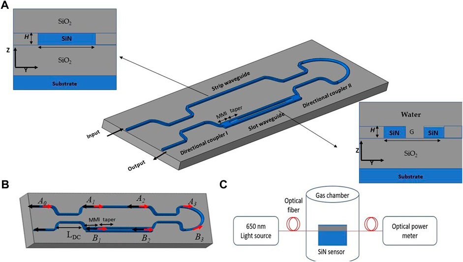
FIGURE 1. (A) Three dimensional view of the proposed sensor and cross setional views of the reference and sensing arm with their strip and slot waveguides. (B) Top view of the LT-MZI gas sensor showing the paths for the light, while marking the mode-converters with dotted-line box. (C) Suggested setup for gas sensing using the proposed sensor.
2 Principle of operation and sensitivity optimization
The sensor structure is illustrated in the isometric view in Figure 1A and the top view in Figure 1B. The incident light beam is split symmetrically between the two MZI arms with a 3-dB directional coupler (DC). The sensor employs a slot waveguide in sensing arm because it has a greater sensitivity than the conventional strip waveguide. However, a strip waveguide is used in the rest of the sensor including the reference arm because the strip waveguide has a smaller attenuation (or power loss). The cross sections of the strip and slot waveguides are shown in Figure 1A insets with widths Wstrip and Wslot, respectively. A multi-mode interference (MMI) optical mode-converter is used as a matching element at the boundaries between the strip and the slot waveguide. Tapering is used to match the mode size as well. The converters are shown in Figure 1A at the beginning and at the end of the sensing arm of the MZI. The MZI is terminated by a 3-dB DC followed by a Sagnac loop mirror, where all incident light beams are reflected. The use of the loop-mirror terminated (LMT) MZI over its conventional equivalent introduces a phase shift between the two arms twice (Parriaux and Veldhuis, 1998). As a result, the performance of the proposed MZI sensor surpasses that of conventional MZI. As will be explained hereinafter, a water medium is used as a cladding to maximize the sensitivity. In this case, the gas detection mechanism is based on that fact that the orientation of water molecules is altered by exposure to a gas, which changes the optical characteristics and refractive index of water (Ho et al., 2013). The suggested setup to sense the gas with water cladding is shown Figure 1C. To make the measurements, an optical graded adhesive can be used to butt-join the waveguide input to an optical fiber. The sensor is put inside a gas chamber. A gas-filled syringe can be used to inject gas into the chamber. Then the chamber is used to evaporate the gas.
The employed waveguide uses the typical SiNOI platform that has a silicon Nitride (SiN) core surrounded by silicon dioxide (SiO2) bottom cladding and a low index top cladding (water). The platform uses a SiN waveguide height, H, of 400 nm for both the strip and slot types while the slot waveguide was implemented using a slot gap, G, of 120 nm to ease fabrication requirements. The DCs have a directional coupler gap, G, as well and a coupler length, LDC, of 7.8 μm. The transmission in each of the output arms is equal to 50% operating at wavelength 650 nm as shown Figure 2A. A colour plot of the field intensity is shown in Figure 2B.
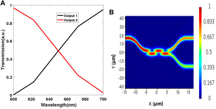
FIGURE 2. (A) The transmission of the two output arms of the DC versus wavelength. (B) Field profile in the DC at a wavelength of 650 nm.
In order to find Wslot that is optimum for the waveguide sensitivity, SWG, of the slot waveguide, the sensitivity was analyzed using finite difference Eigenmode solver while Eq. 1 was used to numerically calculate the waveguide sensitivity (Parriaux and Veldhuis, 1998):
where SWG is the rate of change in the effective index, neff, of the waveguide due to a change in the index of the cover medium. To obtain the maximum waveguide sensitivity, the optical modes and effective indices were investigated. The widths, WSlot and WStrip, were swept from 150 nm to 350 nm for the case when air cladding is used and from 100 nm to 240 nm for the case when water cladding is used with an increment of 10 nm while neff was calculated at each width. The results are depicted in Figure 3A for air and Figure 3B for water. Due to the higher field intensity in the gap area, it is noticed that the slot waveguide consistently achieves higher SWG than the strip waveguide for the same width. It is also observed that the water medium consistently achieves higher SWG than the air medium. Starting with a waveguide width equals to 130 nm and increasing the waveguide width, the waveguide becomes capable of supporting a more confined optical mode. The waveguide sensitivity reaches its peak value when the surrounding evanescent field is maximized. It was found based on the analysis that the maximum evanescent field occurs when the SiN waveguide has a WStrip of 170 nm and WSlot equals to 130 nm in case of water medium as shown Figure 3B. However for air medium, WStrip and WSlot are equal to 230 and 200 nm, respectively as shown Figure 3A. After reaching this point of the maximum waveguide sensitivities, the field becomes more confined inside the core of waveguide, and hence the evanescent field outside of the waveguides decreases. According to these results, it was decided to use water medium instead of air medium for the sensor. Also, the fact that water’s refractive index is nearly identical to that of SiO2 causes an increase in the evanescent field inside the slot region and a consequent increase in the sensitivity. The width of strip waveguide was chosen to be 200 nm to implement the other parts of the sensor because it enables a confined single mode and reduce the propagation loss. The minimum bending raduis was chosen to be 5 µm and the corresponding transmission of a semicircle was found to be larger than 98.8% at 650 nm. A width of 130 nm was selected to be the width of the slot waveguide to increase the sensitivity of the sensing arm. The low waveguide sensitivity for the strip waveguide (∼0.4) when compared with a slot waveguide (∼0.64) is useful for the reduction of the fabrication steps and costs since there is no need for depositing a cladding layer of SiO2 and etching a specific window around the sensing arm. The confinement factor of the TM mode is smaller when thickness of the waveguide is larger than the width. The TM mode exhibits field discontinuity at the core edges in the y direction; as a result, reducing the width over thickness ratio will increase the amount of the evanescent field and, consequently, the sensitivity. Thus, for inexpensive and manufacturable big-feature size sensors, TM mode is better (El Shamy et al., 2022).
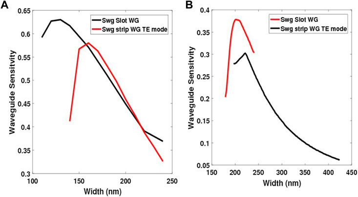
FIGURE 3. (A) Waveguide sensitivity of both strip and slot waveguides as a function of their widths for water cladding. (B) The same but for air cladding.
The coupling losses between the modes are challenging due to the optical mode mismatch between the slot and strip waveguides as shown in Figure 4. A mode-converter is used to switch between the various optical modes to solve this issue. There have been numerous attempts to develop a mode converter that couples the strip and slot modes effectively with low losses (Feng et al., 2007; Deng et al., 2016). The work in ref (Deng et al., 2016). was chosen to be adapted in our LMT-MZI sensor because it has the capability to be easily fabricated using the SiNOI platform. It could demonstrate mode conversion efficiency that is higher than 85%.
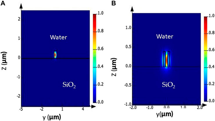
FIGURE 4. The fundamental quasi-TE mode profile for a cross-section of (A) the strip waveguide when Wstrip = 300 nm and (B) the slot waveguide when Wslot = 130 nm.
Three-dimensional finite difference time-domain (3D-FDTD) simulations were used to optimize the optical-mode converter dimensions shown in Figure 5A to reduce the insertion loss (IL) and boost the overall performance. The mode-converter is composed of two sections, an MMI section adjoined with a taper section. As illustrated in the field profile of the converter shown in Figure 5B, the MMI is used to split the input light into two identical beams, in order to change the mode of a strip waveguide into a slot waveguide and vice versa. The taper section gradually pushes the field from the upper high-index region to the low-index region. The simulation results show that the IL is slightly dependent on the taper length, LTaper. As demonstrated in Figure 5C, it was found that for an IL lower than −0.94 dB, the length of the taper section should be longer than 5 μm. Based on this conclusion, the final dimensions for realization the optimized optical mode-converter were designed to be WMMI = 915 nm, LMMI = 960 nm, and LTaper = 10 μm to reach to a good low IL that is close to −0.93 dB.
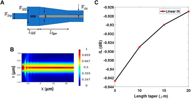
FIGURE 5. (A) The schematic of the mode-converter showing the MMI section and the tapered section. (B) quasi-TE mode profile of the mode-converter, and (C) the insertion loss of the mode-converter as a function of the length of its taper section.
Finally, the phase difference between the two MZI arms, Δϕ, depends on the changes in the medium refractive index and the percentage of evanescent field (Han et al., 2014):
where
3 Results and discussion
The refractive index of the gas is typically very close to 1 with Δn = ngas_water–nwater that is less than 10–3. However, this refractive index can vary depending on the pressure reaching a higher value (Sang and Jeon, 2016). Therefore, the cladding medium index is varied over a wide range from 1.33101 to 1.33901. 3D-FDTD simulations were performed to examine the overall performance of the sensor using different values of the medium index and using different lengths of the sensing arm. It can be shown that the power in the loop mirror paths is given by:
As plotted in Figure 6, it is noticed that the spectra are blue-shifted with increasing the medium index. Figure 7 depicts the shift in the position of the transmittance peaks as they move to the left of the spectrum, and accordingly the intensity of the peak of interest decreases till it reaches a minimum value. The interference pattern shifts, that results from a change in the refractive index (RI) of the detected gas medium, is known as sensitivity. Thus, the overall device sensitivity, S, can be defined as the shift in wavelength due to the change of medium index (Sun et al., 2015):
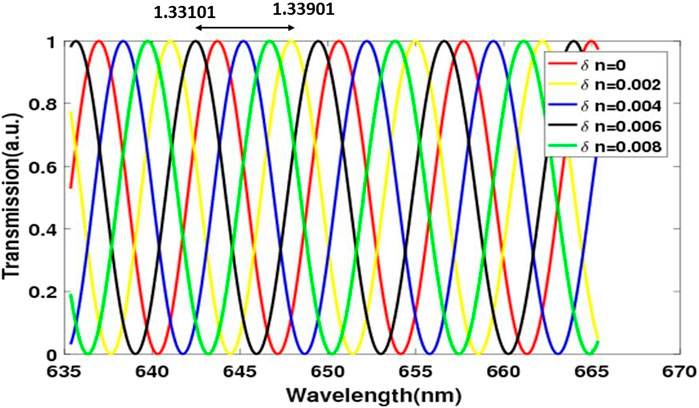
FIGURE 6. The sensor’s spectral shift of output transmittance for the scanned wavelength range with a length of the sensing arm equals to 100 μm and changing three different refractive indices ranging from 1.33101 to 1.33901.
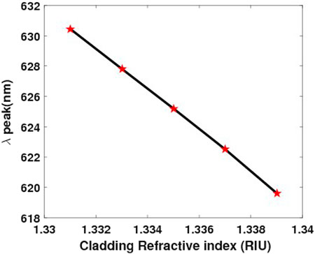
FIGURE 7. Effect of changing the index of the sensed medium on the wavelength of one of the peaks of its interference pattern. The sensed medium index is varied from 1.31097 to 1.31769 with 0.002 increments.
Consequently, the waveguide sensitivity directly impacts the overall sensor sensitivity. Therefore, to increase the sensitivity of the sensor, the waveguide sensitivity had to be maximized. Since the interference of the two MZI arms is involved, the sensor is strongly wavelength dependent. The shift of the wavelength-peaks, ∆λ, as a result from changing the ambient medium RI can be written as:
where FSR is the free spectral range. The FSR and the full-width at half-maximum (FWHM) of the MZI sensor are two main parameters that determines the dynamic range and the resolution of the sensor, respectively. They are given by (Han et al., 2014; El Shamy et al., 2019):
where Δneff = neff,sens − neff,ref, neff, sens and neff,ref are the mode effective indices of the sensing arm and the reference arm, respectively, L is the length of the interferometer arms and λ is the wavelength. Given this and from Eq. 4, one can conclude that the device sensitivity depends on two parameters: the shift in the phase and the FSR in the output spectrum. It should be noted that the phase is also dependent on the length of the sensing arm. This relation could be explained intuitively by noting that the sensitivity is influenced by the fraction of evanescent field outside of the SiN core of the waveguide. Therefore, increasing the sensing arm length leads to an increase in the amount of the interacting evanescent field with the sensed medium that would be the reason of enhancing the overall sensitivity. Nevertheless, to fully assess the performance of any gas sensor, one needs another performance metric given that considering the value of sensitivity to be the only indicator for the quality of the sensor may be misleading. Since both the phase difference and FSR are functions of the length of the sensing arm, a figure of merit (FOM) for the design and optimization of the sensor is the necessary performance criterion to evaluate the performance of the proposed sensor. The FOM accounts for the effect of changes in both device sensitivity and FWHM or FSR of the sensor at the same time. The FOM can be calculated according to the following equation:
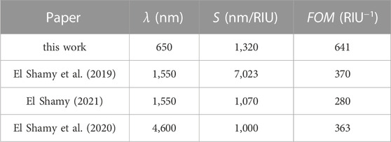
The FOM is carefully examined for the proposed sensor as shown in Figure 8. The analysis inferred from Figure 8 explains that the FOM increases when the difference, Δnmed = n2−n1, between the index of water (n1 = 1.33101), and the medium index (n2) is small. In other words, the FOM is higher when the medium index changes by a small value. Therefore, the smaller index changes of the sensed gas medium, the better the sensor overall performance, and hence, the better gas detection. This result supports the fact that the index of gases changes by very small values. Furthermore, it supports the conclusion that the sensor overall performance is strongly dependent on the length of the MZI sensing arm. From these conclusions, the proposed sensor could reach a FOM value of 641 RIU−1 using only a sensing arm length of 150 μm that corresponds to a device sensitivity equals to 1,320 nm/RIU. This sensitivity and FOM values are compared with the state of the art in Table 1. The FOM of this work is the highest. The design can be modified to operate at a different wavelength. In this case, the waveguide analysis should be repeated and the parameters should be tuned to achieve the optimum waveguide sensitivity at design wavelength.
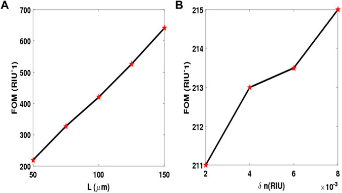
FIGURE 8. (A) The FOM versus the length of the sensing arm of the MZI. (B) The FOM versus the variations in sensing wavelength from water (n1 = 1.33101) to different medium index (n2) using LSensing = 50 μm.
4 Material and methods
The FDTD solves the maxwell’s equation in a non-magnetic material, in three dimensions the FDTD has six electromagnetic components Ex, Ey, Ez and Hx, Hy, and Hz, so the maxwell’s equations is spitted into two independent sets of equations the transverse electric field (TE) and the transverse magnetic field (TM). The TE mode has three components Ex, Ey, Hz and TM also has three components Hx, Hy, Ez. On a discrete spatial and temporal grid each field component in FDTD is solved at a slightly different location within the Yee grid. The rectangular mesh style is used to maintain accuracy. A PML boundary condition is obtained in the FDTD method with the standard method to provide good overall absorption with a relativity small number of layers (Railton and Schneider, 1999).
Three-dimensional FDTD simulation was used for optimizing the DC to get 3-dB output. It was also used for simulating the bending loss of the Sagnac loop and optimizing the converter for maximum efficiency. A mode source with a wavelength range of 600–700 nm was employed. The reflectance and transmittance were extracted using frequency-domain monitors. The boundary conditions were set to perfectly matched layer (PML). For the case of the DC, the simulation was calculated using a window size of 8.5 μm width, a 40 μm length and 2 μm thickness. For the mode convertor, the simulation window used was 3 μm in width, 50 μm in length and 2 μm in thickness. Finally for the Sagnac loop, the simulation window used was 18 μm in width, 32 μm in length and 2 μm in thickness. The waveguide sensitivity, the effective indes and the group index results were extracted from FDE simulations at a wavelength of 650 nm with PML at the boundaries.
5 Conclusion
A novel design is presented for a highly compact SiNOI gas sensor based on MZI interferometer. The refractometric sensor is designed to achieve the maximum waveguide sensitivity, consequently the maximum overall device sensitivity. High values of the sensitivity and FOM have been achieved using smaller lengths of the MZI arms when compared with other similar sensors, which leads to a more compact device. The MZI sensor has been thoroughly analysed and it is proved to be an excellent candidate for a new efficient, ultra-compact and highly miniaturized gas sensor. An overall sensitivity of 1,320 nm/RIU and FOM equals to 641 RIU−1 have been realized using only a sensing arm length of 150 μm at wavelength 650 nm.
Data availability statement
The raw data supporting the conclusion of this article will be made available by the authors, without undue reservation.
Author contributions
ALS: proposed the sensor architecture, conducted the design and simulation, contributed to writing the manuscript and generating the figures. YS: initiated the activity, supervised the work and contributed to writing the manuscript and generating the figure. AHS: supervised the work and provided corrections in the manuscript. ME-A: supervised the work and contributed to writing the manuscript. All authors contributed to the article and approved the submitted version.
Conflict of interest
The authors declare that the research was conducted in the absence of any commercial or financial relationships that could be construed as a potential conflict of interest.
Publisher’s note
All claims expressed in this article are solely those of the authors and do not necessarily represent those of their affiliated organizations, or those of the publisher, the editors and the reviewers. Any product that may be evaluated in this article, or claim that may be made by its manufacturer, is not guaranteed or endorsed by the publisher.
References
Almeida, V. R., Xu, Q., Barrios, C. A., and Lipson, M. (2004). Guiding and confining light in void nanostructure. Opt. Lett. 29 (11), 1209–1211. doi:10.1364/ol.29.001209
Baets, R. (2016). “Silicon photonics: Silicon nitride versus silicon-on-insulator Optical fiber communication conference (America: Optical Society of America).
Barrios, C. A., Gylfason, K. B., Sánchez, B., Griol, A., Sohlström, H., Holgado, M., et al. (2007). Slot-waveguide biochemical sensor. Opt. Lett. 32 (21), 3080–3082. doi:10.1364/ol.32.003080
Deng, Q., Yan, Q., Liu, L., Li, X., Michel, J., and Zhou, Z. (2016). Robust polarization-insensitive strip-slot waveguide mode converter based on symmetric multimode interference. Opt. Express 24 (7), 7347–7355. doi:10.1364/oe.24.007347
Densmore, A., Post, E., Xu, D. X., Waldron, P., Janz, S., Cheben, P., et al. (2006). A silicon-on-insulator photonic wire based evanescent field sensor. IEEE Photonics Technol. Lett. 18 (23), 2520–2522. doi:10.1109/lpt.2006.887374
Dumon, P., Bogaerts, W., Wiaux, V., Wouters, J., Beckx, S., Van Campenhout, J., et al. (2004). Low-loss SOI photonic wires and ring resonators fabricated with deep UV lithography. IEEE Photonics Technol. Lett. 16 (5), 1328–1330. doi:10.1109/lpt.2004.826025
El Shamy, R. S. (2021). Compact gas sensor using silicon-on-insulator loop-terminated mach–zehnder interferometer. Photonics 9, 8. doi:10.3390/photonics9010008
El Shamy, R. S., Khalil, D., and Swillam, M. A. (2020). Mid infrared optical gas sensor using plasmonic Mach-Zehnder interferometer. Sci. Rep. 10 (1), 1293–1299. doi:10.1038/s41598-020-57538-1
El Shamy, R. S., Swillam, M. A., and Khalil, D. A. (2019). Mid infrared integrated MZI gas sensor using suspended silicon waveguide. J. Light. Technol. 37 (17), 4394–4400. doi:10.1109/jlt.2019.2924916
El Shamy, R. S., Swillam, M. A., and Li, X. (2022). Optimization of silicon nitride waveguide platform for on-chip virus detection. Sensors 22 (3), 1152. doi:10.3390/s22031152
Feng, N.-N., Sun, R., Kimerling, L. C., and Michel, J. (2007). Lossless strip-to-slot waveguide transformer. Opt. Lett. 32 (10), 1250–1252. doi:10.1364/ol.32.001250
Gervais, A., Jean, P., Shi, W., and LaRochelle, S. (2018). Design of slow-light subwavelength grating waveguides for enhanced on-chip methane sensing by absorption spectroscopy. IEEE J. Sel. Top. Quantum Electron. 25 (3), 1–8. doi:10.1109/jstqe.2018.2885496
Grist, S. M., Schmidt, S. A., Flueckiger, J., Donzella, V., Shi, W., Talebi Fard, S., et al. (2013). Silicon photonic micro-disk resonators for label-free biosensing. Opt. express 21 (7), 7994–8006. doi:10.1364/oe.21.007994
Han, C., Ding, H., and Lv, F. (2014). Demonstration of a refractometric sensor based on an optical micro-fiber three-beam interferometer. Sci. Rep. 4 (1), 7504–7507. doi:10.1038/srep07504
Ho, W. F., Chan, H. P., and Yang, K. L. (2013). Planar optical waveguide platform for gas sensing using liquid crystal. IEEE Sensors J. 13 (7), 2521–2522. doi:10.1109/jsen.2013.2254596
Hodgkinson, J., and Tatam, R. P. (2012). Optical gas sensing: A review. Meas. Sci. Technol. 24 (1), 012004. doi:10.1088/0957-0233/24/1/012004
Lai, W.-C., Chakravarty, S., Wang, X., Lin, C., and Chen, R. T. (2011). On-chip methane sensing by near-IR absorption signatures in a photonic crystal slot waveguide. Opt. Lett. 36 (6), 984–986. doi:10.1364/ol.36.000984
Liedberg, B., Nylander, C., and Lunström, I. (1983). Surface plasmon resonance for gas detection and biosensing. Sensors actuators 4, 299–304. doi:10.1016/0250-6874(83)85036-7
Parriaux, O., and Veldhuis, G. (1998). Normalized analysis for the sensitivity optimization of integrated optical evanescent-wave sensors. J. Light. Technol. 16 (4), 573–582. doi:10.1109/50.664066
Porcel, M. A., Hinojosa, A., Jans, H., Stassen, A., Goyvaerts, J., Geuzebroek, D., et al. (2019). [INVITED] Silicon nitride photonic integration for visible light applications. Opt. Laser Technol. 112, 299–306. doi:10.1016/j.optlastec.2018.10.059
Poulton, C. V., Byrd, M. J., Raval, M., Su, Z., Timurdogan, E., et al. (2017). Large-scale silicon nitride nanophotonic phased arrays at infrared and visible wavelengths. Opt. Lett. 42 (1), 21–24. doi:10.1364/ol.42.000021
Prieto, F., Sep lveda, B., Calle, A., Llobera, A., Dom nguez, C., Abad, A., et al. (2003). An integrated optical interferometric nanodevice based on silicon technology for biosensor applications. Nanotechnology 14 (8), 907–912. doi:10.1088/0957-4484/14/8/312
Railton, C. J., and Schneider, J. B. (1999). An analytical and numerical analysis of several locally conformal FDTD schemes. IEEE Trans. Microw. Theory Tech. 47 (1), 56–66. doi:10.1109/22.740077
Robinson, J. T., Chen, L., and Lipson, M. (2008). On-chip gas detection in silicon optical microcavities. Opt. Express 16 (6), 4296–4301. doi:10.1364/oe.16.004296
Sang, B. H., and Jeon, T.-I. (2016). Pressure-dependent refractive indices of gases by THz time-domain spectroscopy. Opt. Express 24 (25), 29040–29047. doi:10.1364/oe.24.029040
Sharma, T., Wang, J., Kaushik, B. K., Cheng, Z., Kumar, R., Wei, Z., et al. (2020). Review of recent progress on silicon nitride-based photonic integrated circuits. IEEE Access 8, 195436–195446. doi:10.1109/access.2020.3032186
Sun, X., Dai, D., Thylén, L., and Wosinski, L. (2015). High-sensitivity liquid refractive-index sensor based on a Mach-Zehnder interferometer with a double-slot hybrid plasmonic waveguide. Opt. express 23 (20), 25688–25699. doi:10.1364/oe.23.025688
Tetz, K. A., Pang, L., and Fainman, Y. (2006). High-resolution surface plasmon resonance sensor based on linewidth-optimized nanohole array transmittance. Opt. Lett. 31 (10), 1528–1530. doi:10.1364/ol.31.001528
Vlasov, Y. A., and McNab, S. J. (2004). Losses in single-mode silicon-on-insulator strip waveguides and bends. Opt. express 12 (8), 1622–1631. doi:10.1364/opex.12.001622
Wilmart, Q., El Dirani, H., Tyler, N., Fowler, D., Malhouitre, S., Garcia, S., et al. (2019). A versatile silicon-silicon nitride photonics platform for enhanced functionalities and applications. Appl. Sci. 9 (2), 255. doi:10.3390/app9020255
Xuan, Y., Liu, Y., Varghese, L. T., Metcalf, A. J., Xue, X., Wang, P. H., et al. (2016). High-Q silicon nitride microresonators exhibiting low-power frequency comb initiation. Optica 3 (11), 1171–1180. doi:10.1364/optica.3.001171
Keywords: refractive index, MMI, MZI, photonics sensor, sensitivity
Citation: Sultan A, Sabry YM, Samir A and El-Aasser MA (2023) Mirror-terminated Mach-Zehnder interferometer based on SiNOI slot and strip waveguides for sensing applications using visible light. Front. Nanotechnol. 5:1121537. doi: 10.3389/fnano.2023.1121537
Received: 11 December 2022; Accepted: 13 April 2023;
Published: 26 April 2023.
Edited by:
Yefeng Yu, Nanjing University of Science and Technology, ChinaCopyright © 2023 Sultan, Sabry, Samir and El-Aasser. This is an open-access article distributed under the terms of the Creative Commons Attribution License (CC BY). The use, distribution or reproduction in other forums is permitted, provided the original author(s) and the copyright owner(s) are credited and that the original publication in this journal is cited, in accordance with accepted academic practice. No use, distribution or reproduction is permitted which does not comply with these terms.
*Correspondence: Yasser M. Sabry, eWFzc2VyLnNhYnJ5QGVuZy5hc3UuZWR1LmVn
 Alaa Sultan
 Yasser M. Sabry
 Ahmed Samir1